How Does LiDAR PCB Manufacturing Affect Sensor Performance and Reliability?
LiDAR PCB manufacturing affects signal integrity, receiver sensitivity, timing accuracy, thermal stability, and long-term reliability. Shenzhen Hongda Circuit Technology Co., Ltd. supports precision PCB fabrication and PCBA manufacturing for complex electronic assemblies, with process selection based on the LiDAR architecture, electrical requirements, mechanical constraints, and production volume.
What Does LiDAR PCB Manufacturing Include?
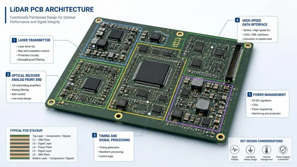
LiDAR PCB Manufacturing Architecture Showing Transmitter, Receiver, Timing and Power Circuits
LiDAR PCB manufacturing includes bare-board fabrication, component assembly, inspection, electrical verification, and—where the project requires it—functional testing of the electronics supporting laser transmission, optical reception, timing, data processing, and power management.
LiDAR is not a single PCB application. A sensor may contain separate transmitter and receiver boards, a combined mixed-signal board, a processor board, a power-management board, or a rigid-flex interconnection connecting multiple subassemblies. The manufacturing route should follow the actual architecture rather than the product name alone.
| LiDAR circuit section | Main electrical or manufacturing concern | What the PCB supplier should review |
|---|---|---|
| Laser transmitter | Fast current transitions, switching-loop inductance, local heating | Copper geometry, return paths, via capacity, thermal path |
| Optical receiver | Low-level signals, noise coupling, detector bias | Ground reference, routing separation, surface contamination risks |
| Timing and conversion | Clock quality, channel matching, signal integrity | Stackup, reference planes, controlled-impedance requirements |
| FPGA, processor or interface | Fine-pitch packages and high-speed interfaces | BGA escape routing, via structures, layer count |
| Power management | Voltage conversion, ripple, current density | Copper thickness, plane design, thermal dissipation |
| Mechanical interface | Compact enclosure, connectors, optical alignment constraints | Board outline, thickness, warpage, mounting and keep-out zones |
The manufacturing requirements differ by architecture. A time-of-flight (ToF) sensor, a flash LiDAR module, a MEMS-based scanning system, and an FMCW LiDAR design do not automatically require the same stackup, materials, or interconnection technology.
For procurement, the first question is therefore not “Can the supplier manufacture LiDAR PCBs?” It is “Can the supplier manufacture this board construction and demonstrate that the agreed requirements have been met?”
Which PCB Design Requirements Matter Most for LiDAR Performance?
The most important requirements are transmitter-to-receiver isolation, low-noise analog routing, timing and signal-integrity control, stable power delivery, thermal management, and manufacturable interconnections. Their relative importance depends on the detector, laser-driver design, data interface, and mechanical packaging.
How should the transmitter and receiver be isolated?
The transmitter may generate fast current transitions while the receiver processes much smaller signals. If both sections share an unsuitable return-current path, switching noise can couple into the receiver and contribute to false detections, unstable measurements, or reduced usable range.
The design review should examine:
- The complete high-current switching loop, including its return path.
- The physical relationship between the laser driver and sensitive receiver inputs.
- Ground-plane continuity and the actual return-current paths.
- Placement of switching regulators, clock sources, and noisy digital interfaces.
- Detector-bias filtering and decoupling requirements.
- The effectiveness of shielding, grounding, and via stitching where applicable.
Engineering note: A split ground plane is not a universal solution. An arbitrary gap in the reference plane can force high-frequency return current to take a longer path and increase coupling. The layout should be evaluated as a current-return system, not simply divided into labeled analog and digital areas.
How should sensitive receiver routing be controlled?
The receiver front end may use an avalanche photodiode (APD), a single-photon avalanche diode (SPAD), a silicon photomultiplier (SiPM), or another detector architecture. These devices have different bias, noise, and interface requirements.
For sensitive inputs, the design team should specify the allowed parasitic capacitance, routing length, return reference, bias noise, and relationship to adjacent switching signals. Where a transimpedance amplifier (TIA) is used, its feedback network and detector interconnection deserve particular attention because stray capacitance can affect bandwidth and stability.
There is no single spacing rule suitable for every LiDAR board. A defensible spacing requirement should be derived from the circuit sensitivity, switching spectrum, stackup, enclosure, and available isolation structures.
When is controlled impedance necessary?
Controlled impedance is necessary when the interface and edge rates make transmission-line behavior significant—for example, certain high-speed processor links, differential interfaces, or RF paths.
It is not necessary to specify controlled impedance for every net on every LiDAR board. The engineering team should identify which nets need a defined impedance, their target values, reference layers, routing geometry, and acceptable tolerance.
PCBKR provides impedance-controlled PCB manufacturing and high-precision fabrication capabilities. The final trace geometry and impedance tolerance must be confirmed against the selected laminate, copper thickness, finished stackup, and design rules.
Related capability: Impedance-Controlled PCB Manufacturing.
Which Materials, Layer Counts, and HDI Structures Should LiDAR OEMs Choose?
Select materials and interconnection structures according to signal loss, dielectric stability, thermal requirements, mechanical constraints, package pitch, and cost. LiDAR does not automatically require Rogers laminates, HDI, rigid-flex, or a particular number of layers.
How should OEMs compare FR-4, high-Tg, and low-loss materials?
| Material approach | Potential advantages | Main qualification questions |
|---|---|---|
| Standard FR-4 | Cost-effective and widely available | Is its electrical performance adequate for the actual interface and temperature range? |
| High-Tg FR-4 | Can offer a suitable process and thermal-performance balance | Does the specific laminate meet the assembly and environmental requirements? |
| Low-loss laminate | Useful when dielectric loss or electrical stability is a meaningful design constraint | Is the benefit justified by frequency, route length, edge rate, and system budget? |
| Hybrid stackup | Allows different material systems to serve different electrical needs | Are bonding, thermal expansion, registration, and fabrication compatibility controlled? |
| Rigid-flex | Can reduce connector count and accommodate complex packaging | Does the design justify the added bend, material, and reliability constraints? |
The optical wavelength—such as 905 nm or 1550 nm—does not by itself determine the PCB laminate. Material selection should follow the electrical characteristics of the circuitry and the system’s thermal and mechanical requirements.
A low-loss material may be justified for a demanding high-speed or RF path, but it can add material cost, lead time, and fabrication complexity. For a predominantly low-speed control board, a qualified FR-4 construction may be more appropriate.
Does every LiDAR PCB require HDI technology?
No. HDI is valuable when fine-pitch packages, compact dimensions, routing density, or layer-transition requirements cannot be met efficiently with conventional multilayer construction.
Before specifying HDI, evaluate:
- Component pitch and breakout geometry.
- Available routing channels and total layer count.
- Finished microvia diameter and aspect ratio.
- Blind, buried, stacked, or staggered via requirements.
- Via-in-pad and copper-fill requirements.
- Registration, dielectric thickness, and reliability expectations.
- Whether the design can be simplified to reduce fabrication cost.
For example, a compact receiver board with fine-pitch BGAs may need microvias to escape the package without excessive layer count. A larger power board with conventional packages may be better served by a standard multilayer construction with suitable copper thickness.
PCBKR offers advanced HDI manufacturing capabilities. The required build-up structure and feature dimensions should be assessed during design-for-manufacturing (DFM) review rather than selected simply because HDI is considered an advanced technology.
Related capability: Advanced HDI PCB Manufacturing.
Which stackup parameters must be fixed before production?
At minimum, the RFQ or fabrication specification should identify:
- Total layer count and finished board thickness.
- Copper weight by layer.
- Dielectric materials and target dielectric thicknesses.
- Controlled-impedance nets and tolerance.
- Microvia and through-via structures.
- Minimum trace width and spacing.
- Surface finish and solder-mask requirements.
- Board outline, dimensional tolerances, and warpage criteria.
A stackup is not fully qualified by listing material brand names alone. Actual dielectric thickness, copper geometry, lamination behavior, and finished-board measurements determine whether the manufactured board matches the electrical design.
How Do Modern PCB Manufacturing Technologies Improve LiDAR Board Manufacturability?
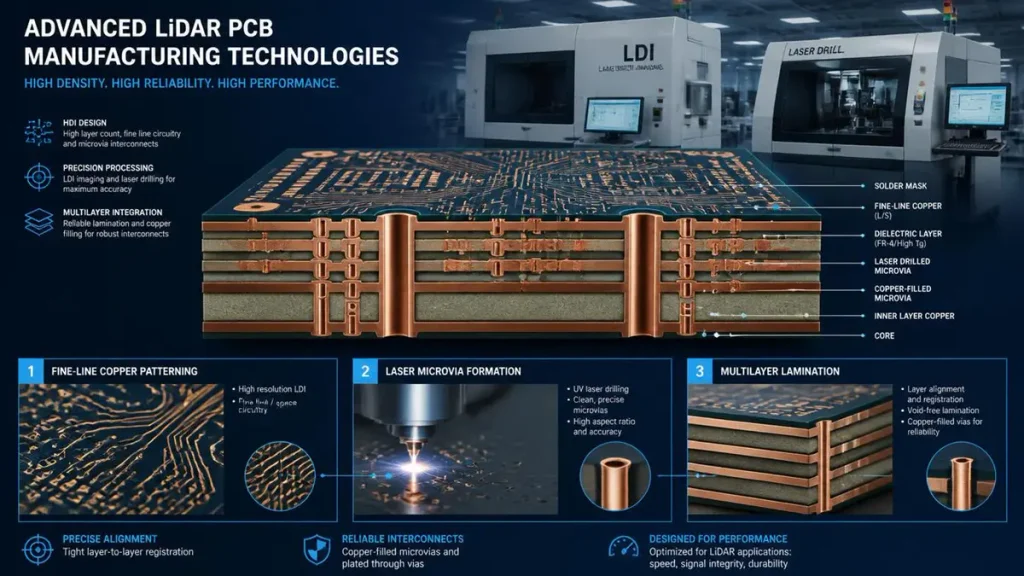
LiDAR PCB Manufacturing Using HDI Microvias, Laser Drilling, LDI and Fine-Line Copper Processing
Laser Direct Imaging (LDI), laser drilling, fine-line processes such as mSAP, controlled lamination, and risk-based inspection can improve pattern definition, interconnect density, dimensional control, and defect detection. Each technology addresses different failure modes; none independently guarantees finished-board performance.
Shenzhen Hongda Circuit Technology Co., Ltd. has reported the following equipment and process capabilities. These are manufacturing reference points, not a blanket promise that every value is achievable on every LiDAR construction.
| Equipment or process | Company-reported capability | Potential relevance to LiDAR PCB projects |
|---|---|---|
| SCREEN Ledia LDI | 8 µm process reference; ±10 µm registration reference | Fine-pattern imaging and registration control, subject to the actual process window |
| Mitsubishi UV/CO₂ laser | 75 µm microvia reference with ±5 µm positional reference | Laser-drilled interconnects for suitable HDI designs |
| Picosecond laser processing | 50 µm feature reference | Precision processing for qualified applications |
| mSAP fine-line processing | 8/8 µm line/space capability reference | High-density routing where package escape or compact layout justifies it |
| LAUFFER lamination equipment | Reported pressure capability of 80, 150, and 200 psi; vacuum below 50 mbar | Lamination control for complex multilayer constructions, subject to material and recipe qualification |
| AOI and X-ray inspection | Available inspection methods | Detection of surface-pattern and selected hidden-structure defects |
| Flying-probe and four-wire Kelvin testing | Available electrical verification methods | Electrical continuity/isolation checks and low-resistance measurement where appropriate |
These figures must be checked against the specific construction, copper thickness, board dimensions, material system, and acceptance criteria. For example, an 8/8 µm fine-line process reference does not mean every 8/8 µm layout is suitable for every copper thickness or has the same production yield.
Why does LDI matter for fine-line PCB manufacturing?
LDI exposes circuit patterns digitally and avoids the phototool limitations of conventional exposure. In fine-line designs, the important outcome is not merely the nominal feature size; it is whether trace geometry, registration, and spacing remain within the qualified process window across the panel.
For LiDAR boards with dense BGA fanout or compact mixed-signal routing, the DFM review should verify the minimum finished trace width, spacing after etching or plating, copper thickness, and the available manufacturing margin.
When does laser drilling become useful?
Laser drilling can create small microvias for HDI interconnections. Its usefulness depends on the target diameter, dielectric material, via depth, capture-pad geometry, and subsequent desmear, metallization, and copper-filling processes.
A 75 µm microvia reference should not be interpreted as proof that every 75 µm via can be used in any stackup. Via depth, aspect ratio, landing-pad dimensions, registration tolerance, and reliability requirements must also be reviewed.
What does mSAP contribute to a compact LiDAR board?
Modified semi-additive processing can support fine-line copper formation for dense routing. However, the final result depends on imaging, seed-layer formation, plating, flash etching, copper thickness, and inspection.
If the design can be routed using conventional subtractive processing, mSAP may add cost without providing a meaningful benefit. It becomes more relevant when package density and routing constraints justify its process complexity.
Why is lamination control important?
Multilayer and HDI fabrication involves resin flow, dielectric thickness, interlayer registration, copper bonding, and thermal-expansion behavior. Variations can affect impedance, dimensional stability, and interconnect reliability.
The correct approach is to qualify a lamination cycle for the selected material and stackup, then verify critical characteristics through suitable dimensional measurements, cross-sections, and electrical tests. Equipment pressure or vacuum specifications alone do not prove that a particular board has been manufactured correctly.
Which PCBA Assembly and Inspection Processes Should a LiDAR Supplier Provide?
A suitable PCBA process should combine controlled component placement and soldering with inspection and electrical or functional tests selected for the board’s risks. AOI, X-ray, bare-board electrical testing, and functional testing are complementary methods, not interchangeable guarantees.
For a LiDAR receiver board, a solder joint can appear acceptable externally while a hidden BGA connection remains defective. Conversely, a visually sound assembly may still fail because of an incorrect component, polarity error, noisy power rail, or unstable analog front end.
| Process or test | What it can help verify | What it does not prove by itself |
|---|---|---|
| Solder paste inspection (SPI), where used | Deposited paste volume and placement | Final solder-joint integrity |
| AOI | Visible component placement, polarity, and selected solder defects | Hidden BGA joints or electrical functionality |
| X-ray | Hidden solder-joint structures and selected internal defects | Correct firmware, optical alignment, or full sensor performance |
| Bare-board electrical test | Continuity and isolation against the specified test data | Correct analog performance after assembly |
| Flying-probe test | Electrical checks without a dedicated fixture, useful for suitable prototype and low-volume boards | Full functional behavior under operating conditions |
| TDR or other impedance verification | Controlled-impedance characteristics when properly specified and measured | Complete end-to-end signal integrity in the final system |
| Functional test (FCT) | Defined electrical and operational behavior under the test setup | Every field condition or full optical performance unless explicitly included |
The inspection plan should be driven by package type, component pitch, product risk, manufacturing volume, and the customer’s acceptance criteria. “100% inspection” is meaningful only when the inspected characteristics and acceptance limits are defined.
What should a LiDAR functional test actually cover?
The test plan should match the product’s requirements and the equipment available. Depending on the assembly, it may include:
- Power-rail voltage, current, and startup behavior.
- Communication interfaces and firmware loading.
- Laser-driver control and interlock signals.
- Receiver bias and analog-front-end checks.
- Timing or data-interface validation.
- Temperature-related checks, where specified.
- Optical transmitter/receiver tests using the customer’s approved fixtures.
- Traceability of test results to board serial numbers or production lots.
A PCB assembler should not claim to have validated LiDAR range accuracy or optical performance simply because it completed AOI and X-ray. Those tests inspect assembly characteristics; optical range, point-cloud quality, and system-level accuracy require the appropriate sensor, calibration process, optical setup, and test criteria.
How Should LiDAR PCB Reliability and Qualification Be Verified?
Reliability qualification should connect the product’s operating environment and failure risks to explicit test methods, sample sizes, acceptance criteria, and documented results. Automotive, industrial, robotics, and surveying applications may require different qualification plans.
Before quoting, the OEM should define the expected temperature range, vibration and shock environment, operating lifetime, humidity exposure, power cycling, mechanical constraints, and consequences of failure.
Potential qualification activities include:
- Thermal cycling or thermal shock according to the agreed product specification.
- Temperature and humidity exposure where relevant.
- Mechanical vibration and shock testing.
- Microvia and plated-through-hole reliability evaluation.
- Solder-joint and package-level reliability checks.
- Dimensional and warpage verification.
- Electrical continuity and insulation verification.
- Functional retesting after environmental exposure.
Not every test is required for every LiDAR PCB. Test selection should follow the applicable customer specification, product risk, and contractual qualification plan.
Important standards distinction: AEC-Q100 addresses integrated-circuit qualification, and AEC-Q200 addresses passive electronic components. They are not general certifications for bare PCBs. OEMs should separately define the required PCB fabrication specification, PCBA workmanship criteria, component qualifications, and system-level validation.
Which manufacturing records should buyers request?
For a production-intent build, request records that demonstrate the agreed requirements have actually been checked:
- Approved fabrication drawing and stackup.
- Material identification and applicable material certificates.
- Bare-board electrical test results.
- Dimensional and, where applicable, impedance reports.
- Microsection or interconnect-reliability evidence when required.
- Assembly inspection and defect records.
- Functional test results against the approved test procedure.
- Lot or serial-number traceability and revision identification.
- Nonconformance handling and corrective-action records, when applicable.
A certificate or equipment list is not a substitute for product-specific evidence. The most useful qualification package links each critical requirement to its inspection or test method and records the result.
What Determines LiDAR PCB Manufacturing Cost and Lead Time?
LiDAR PCB cost and lead time depend on board size, layer count, material availability, copper construction, fine-line and microvia requirements, fabrication yield, component sourcing, assembly complexity, inspection coverage, and qualification scope. The exact cost and schedule can only be established after reviewing the project data.
| Cost or lead-time driver | Why it matters | How buyers can reduce avoidable cost |
|---|---|---|
| Layer count and stackup | More layers and complex laminations increase process steps | Confirm the minimum stackup that meets electrical and mechanical requirements |
| HDI and microvias | Additional laser, plating, filling, and inspection operations may be required | Use microvias only where routing or package escape requires them |
| Fine-line copper | Tight geometries can narrow the process window and affect yield | Review finished copper thickness and manufacturability together |
| Specialty materials | Some laminates have longer sourcing times or minimum order constraints | Approve alternatives only after electrical and thermal review |
| Surface finish | Finish selection affects assembly, contact performance, and cost | Specify the finish that matches the component and application requirements |
| Component sourcing | Long-lead, obsolete, or restricted parts can delay assembly | Provide an approved BOM and permitted substitutions early |
| Testing and qualification | Custom fixtures and environmental tests add cost and time | Define test coverage and acceptance criteria before quotation |
| Prototype-to-production transition | Uncontrolled revisions can create rework and repeat qualification | Freeze approved data and manage engineering changes formally |
A low prototype price may not reflect the total cost of moving to production. A better comparison considers engineering review, first-article quality, test coverage, yield risks, documentation, and the cost of repeating builds after avoidable design or process problems.
OEMs should request separate pricing for bare PCB fabrication, PCBA, tooling or test fixtures, special inspection, and qualification work where applicable. This makes supplier quotations easier to compare and exposes scope differences before purchase orders are issued.
How Can OEM Buyers Evaluate a LiDAR PCB Manufacturer?
Buyers should assess a supplier using evidence of process capability, design-for-manufacturing support, inspection coverage, traceability, communication quality, and a credible path from prototype to repeat production—not equipment claims alone.
Shenzhen Hongda Circuit Technology Co., Ltd. provides PCB fabrication capabilities covering high-precision and HDI constructions, along with PCBA manufacturing options. The appropriate process and test scope should be confirmed against the actual LiDAR design during RFQ and engineering review.
What should be reviewed before the first order?
1. Manufacturing capability fit
Ask the supplier to review the actual layer count, finished copper, line/space, microvia structure, board thickness, impedance requirements, and material system. Request a written capability confirmation for the specific design.
2. DFM feedback quality
A useful DFM review identifies concrete risks: insufficient annular ring, tight microvia landing geometry, unsuitable copper thickness for fine lines, inadequate solder-mask clearance, high-risk BGA escape routing, or a stackup that cannot meet the requested impedance.
3. Inspection and test coverage
Ask which defects each method detects, which characteristics are measured, and what records will be supplied. AOI, X-ray, electrical testing, and functional testing should have clearly defined purposes.
4. Revision and traceability control
Confirm how Gerber or ODB++ revisions, BOM changes, approved stackups, firmware versions, test limits, and production lots are controlled. A board built to an obsolete revision can pass its own inspection and still be unusable in the final product.
5. Prototype-to-production planning
Ask how first-article findings are documented, how process changes are approved, and what evidence is required before volume production. A controlled transfer should preserve the approved materials, construction, test methods, and acceptance criteria.
What information should be included in a LiDAR PCB RFQ?
For a meaningful quotation, provide as much of the following as is available:
- Gerber, ODB++, IPC-2581, or approved manufacturing data.
- Stackup, layer count, board thickness, and copper weight.
- Minimum trace/space and via dimensions.
- Controlled-impedance requirements and target tolerances.
- Material and surface-finish requirements.
- Board quantity, prototype quantity, and expected annual demand.
- BOM, approved manufacturers, and component substitution rules for PCBA.
- Assembly drawing, polarity, and special handling requirements.
- Required AOI, X-ray, electrical, functional, and environmental tests.
- Target delivery date and any qualification or documentation requirements.
If some details are not finalized, identify them as open engineering decisions rather than leaving them ambiguous. This allows the supplier to distinguish a budgetary quotation from a production-ready proposal.
For manufacturing review, contact Shenzhen Hongda Circuit Technology Co., Ltd. at pcb@pcbkr.com or visit PCBKR.
What Questions Do Procurement Teams Ask When Searching for a LiDAR PCB Supplier?
Procurement teams should focus on whether a supplier can manufacture the specified construction, assemble the required components, document quality, support engineering changes, and scale from prototypes to repeat orders.
Can one supplier handle both LiDAR PCB fabrication and PCBA assembly?
Yes, a supplier offering both services can coordinate fabrication and assembly under a common project workflow. Buyers should still confirm whether both processes are performed in-house or partly subcontracted, who controls revisions, and which inspection and test records are included.
How do I compare quotes from LiDAR PCB manufacturers?
Compare identical technical scope: stackup, materials, copper thickness, microvia structures, surface finish, assembly BOM, inspection coverage, functional tests, quantity, and delivery terms. A lower quotation may exclude engineering review, special testing, or documentation required for qualification.
What files are needed to request a LiDAR PCB and PCBA quotation?
For bare PCB fabrication, provide manufacturing data, stackup, fabrication drawing, and critical acceptance requirements. For PCBA, also provide the BOM, assembly drawing, approved part alternatives, quantities, and test requirements. Identify unresolved design details so the supplier can flag quotation assumptions.
How can I verify the quality of a LiDAR PCB supplier?
Request capability confirmation for your actual design, sample inspection records, electrical test coverage, relevant material documentation, traceability procedures, and—where required—microsection, impedance, reliability, or functional test results. Confirm that certificates apply to the relevant facility, process, and product scope.
Can a LiDAR PCB supplier support prototypes and mass production?
A supplier may support both, but the transition should be qualified rather than assumed. Confirm how first-article findings are resolved, production data are frozen, component sourcing is controlled, process changes are approved, and repeat lots are checked against the same acceptance criteria.
Conclusion: How Should You Select a LiDAR PCB Manufacturing Partner?
LiDAR PCB manufacturing requires coordinated decisions across electrical design, material selection, interconnection technology, fabrication, assembly, and verification. The most advanced process is not necessarily the best one; the right choice is the least complex, reliably manufacturable construction that meets the product’s electrical, mechanical, environmental, and production requirements.
For Shenzhen Hongda Circuit Technology Co., Ltd., the practical starting point is a project-specific DFM and RFQ review. By confirming the required stackup, fine-line and microvia structures, material system, assembly scope, and test evidence before production, OEM buyers can reduce avoidable rework and make supplier comparisons more meaningful.
Request a LiDAR PCB manufacturing review: Send your PCB data, stackup, BOM (if assembly is required), target quantity, and testing requirements to pcb@pcbkr.com.
About Author
David Chen LinkedIn Profile
David Chen is a Senior RF/PCB Process Engineer at Shenzhen Hongda Circuit Technology Co., Ltd., with over 12 years of experience in high-frequency PCB fabrication, impedance-controlled stack-up design, and Rogers/PTFE laminate processing. He also boasts an extensive professional background in PCBA manufacturing, PCBA testing, and PCBA optimization, with specialized expertise in high-precision PCBA fault analysis and rigorous PCBA reliability testing. The author has worked with high-layer-count server PCB fabrication, ultra-low-loss backplane stackups, and thermo-mechanical reliability optimization for AI infrastructure projects involving 112G and 224G PAM4 architectures. Skilled in complex circuit design and cutting-edge advanced PCB manufacturing processes, he delivers solutions that elevate product durability and performance across industrial applications. His technical articles focusing on PCBA manufacturing workflows and testing methodologies are widely cited by industry peers and technical platforms, and have gained attention and recognition from industry colleagues.