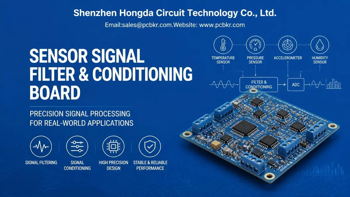
Sensor Signal Filter & Conditioning Board: Design, Manufacturing and OEM Sourcing
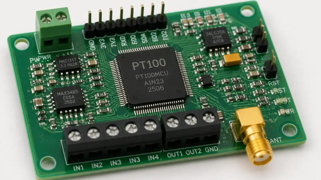
PCB Material: FR-4 / High-Tg FR-4 / Low-Noise Circuit-Compatible PCB Materials
Layers: 2–8 Layers (design-dependent)
Board Thickness: Customized
Copper Thickness: Customized
Minimum Trace Width / Spacing: Customized
Minimum Hole Size: Customized
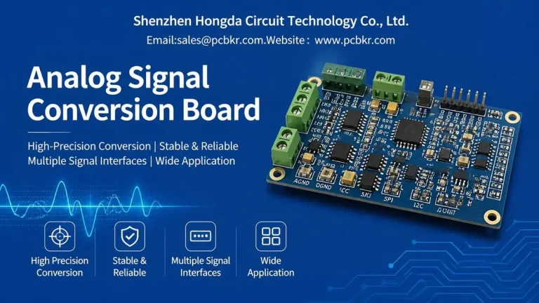
A Sensor Signal Filter & Conditioning Board converts raw sensor outputs into stable, filtered, and measurable signals for downstream controllers, processors, and data acquisition systems. It integrates signal acquisition, analog front-end conditioning, active and passive filtering, low-noise amplification, ADC interfacing, and noise-control measures. For OEMs, reliable performance depends on both circuit design and consistent PCB fabrication and PCBA assembly.
For industrial equipment, measurement instruments, automation systems, medical devices, and embedded electronics, sensor signals often require amplification, filtering, protection, isolation, or level adjustment before digital conversion. A properly engineered signal conditioning board helps manage these requirements while supporting stable operation across different electrical and environmental conditions.
Shenzhen Hongda Circuit Technology Co., Ltd. provides custom PCB fabrication and PCBA assembly services for electronic control and signal-processing applications. From prototype development to small-batch and volume production, PCBKR supports OEM projects requiring coordinated PCB manufacturing, component assembly, and manufacturing quality control.
1. Sensor Signal Conditioning Board Architecture and Core Functions
A Sensor Signal Filter & Conditioning Board is an electronic interface between a physical sensor and a processing system. Its purpose is to adapt the sensor’s electrical output to the input requirements of an ADC, microcontroller, PLC, embedded processor, or measurement instrument.
A typical signal path includes:
Sensor Input → Input Protection → Signal Conditioning → Filtering → Amplification → ADC Interface → Digital Processing
The actual circuit architecture depends on the sensor technology, signal amplitude, output impedance, measurement bandwidth, accuracy requirements, and operating environment.
| Functional block | Main engineering purpose | Typical circuit elements |
|---|---|---|
| Sensor input | Receives the electrical output from the sensor | Connectors, terminal blocks, input networks |
| Input protection | Limits electrical stress and transient interference | TVS diodes, series resistors, protection networks |
| Signal conditioning | Adjusts signal level, impedance, and offset | Op-amps, instrumentation amplifiers, resistor networks |
| Signal filtering | Reduces unwanted frequency components | RC filters, active filters, LC networks |
| Low-noise amplification | Amplifies small sensor signals | Low-noise op-amps, instrumentation amplifiers |
| ADC interface | Prepares signals for digital conversion | ADC drivers, reference circuits, input filters |
| Power management | Supplies stable power to analog and digital sections | LDOs, DC-DC converters, decoupling networks |
| Communication interface | Transfers acquired data to the main controller | SPI, I²C, UART, CAN, RS-485 |
Not every application needs all these functional blocks. A simple voltage sensor interface may only require input protection, a resistor divider, and an RC filter. A high-resolution strain gauge acquisition system may need a precision excitation source, instrumentation amplifier, differential filtering, stable reference, and a high-resolution ADC.
For OEM projects, the most important early decision is to define the complete sensor signal chain rather than select individual components independently.
2. Sensor Signal Acquisition for Different Sensor Technologies
Sensor signal acquisition begins with understanding the electrical characteristics of the sensor. Different sensor technologies produce different signal levels, impedances, output formats, and noise characteristics. These differences directly influence the input circuit, protection design, amplification stage, and ADC configuration.
Voltage and Current Output Sensors
Industrial sensors commonly provide voltage or current outputs, including 0–5 V, 0–10 V, and 4–20 mA signals.
A voltage input circuit may require:
- Input voltage scaling to match the ADC range
- Overvoltage and reverse-polarity protection
- Input impedance management
- RC filtering for high-frequency interference
- Buffering where the source impedance is unsuitable
For 4–20 mA inputs, a precision shunt resistor converts current into voltage. The resistor value must be selected according to the input range of the conditioning circuit and ADC.
For example, a 250 Ω shunt converts a 4–20 mA signal into 1–5 V. The resulting voltage range must still be checked against the ADC input limits, amplifier common-mode range, and fault conditions.
Thermocouple and RTD Sensors
Thermocouples generate small voltage signals related to temperature differences. Their low-level outputs make them sensitive to electrical interference, input offset, and unwanted thermoelectric voltages.
Typical circuit considerations include:
- Low-offset and low-drift amplification
- Differential input measurement
- Cold-junction compensation for thermocouples
- Input filtering and transient protection
- Careful connector and copper-junction design
RTD sensors, including PT100 and PT1000 devices, generally require a measurement circuit that supplies a controlled excitation current and measures the resulting voltage.
The excitation current must be selected to balance measurement sensitivity against self-heating. For precision applications, reference stability, lead-wire resistance, and measurement topology must also be considered.
Strain Gauge and Bridge Sensors
Load cells, pressure transducers, and force sensors often use Wheatstone bridge structures. Their output signals may be only a few millivolts, depending on the excitation voltage and sensor sensitivity.
A typical acquisition circuit includes:
- Stable bridge excitation
- Differential instrumentation amplification
- High common-mode rejection
- Low-noise filtering
- ADC input compatibility
- Temperature and offset compensation where required
Ratiometric measurement can help reduce errors caused by excitation variation when the ADC reference and sensor excitation are appropriately related.
Piezoelectric and High-Impedance Sensors
Piezoelectric sensors and other high-impedance sensing elements require special attention to input leakage, parasitic capacitance, and amplifier bias current.
Depending on the sensor, the interface may use a charge amplifier, voltage amplifier, or dedicated analog front-end circuit.
Important design considerations include:
- Low-input-bias-current amplifiers
- Short, controlled high-impedance signal paths
- Guard rings where appropriate
- Low-leakage protection components
- Suitable PCB surface cleanliness
- Stable feedback components
Flux residue, moisture, contamination, and inappropriate protection components can create leakage paths that affect sensitive measurements. These issues must be considered during both PCB design and PCBA process planning.
Capacitive and MEMS Sensors
Capacitive sensors and MEMS devices may produce small analog signals or require specialized excitation and readout circuits.
The interface design must account for parasitic capacitance, sensor bandwidth, mechanical noise, supply sensitivity, and the characteristics of the selected sensor IC.
The acquisition architecture should be defined around the actual sensor datasheet and system measurement requirements rather than a generic signal conditioning circuit.
3. Analog Front-End Conditioning and Signal Adaptation
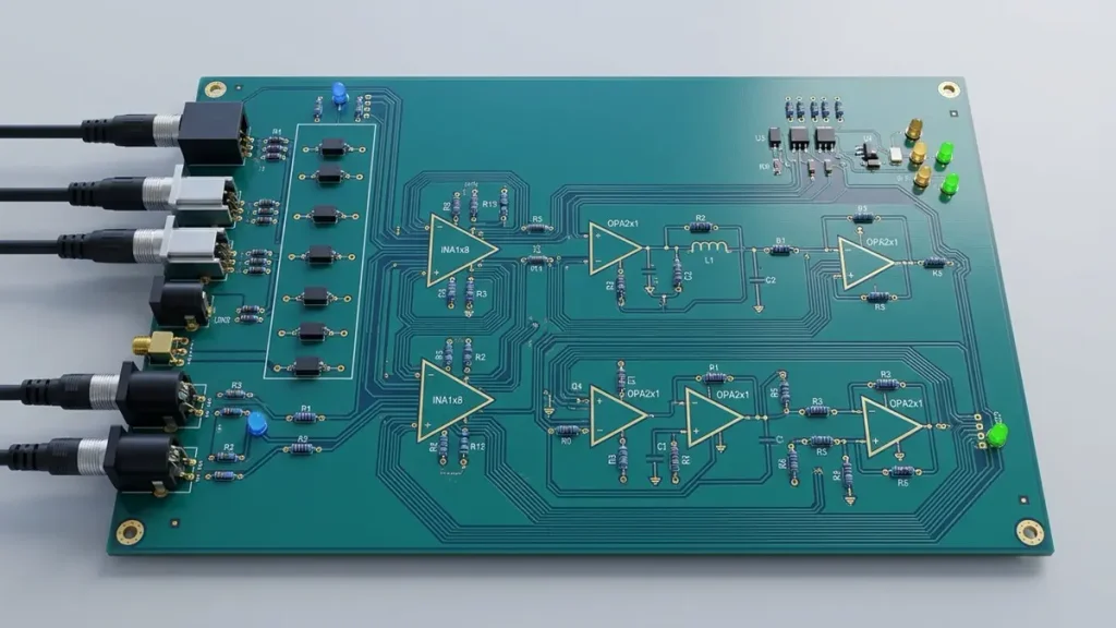
Sensor Signal Filter & Conditioning Board analog front-end with operational amplifiers and precision signal conditioning components
The analog front end (AFE) prepares sensor signals for accurate measurement. Its primary functions include impedance matching, amplification, level shifting, buffering, differential measurement, and input protection.
A well-designed AFE prevents the sensor signal from being distorted before it reaches the filtering and conversion stages.
Input Impedance and Buffering
The input impedance of the conditioning circuit should be compatible with the sensor’s output impedance.
If the receiving circuit loads the sensor excessively, the measured signal may be reduced or distorted. A buffer amplifier can isolate the sensor from downstream circuit loading.
For high-impedance sensors, amplifier input bias current and PCB leakage can become significant error sources.
Gain and Offset Adjustment
Sensor outputs may be too small or have an offset that does not match the ADC input range.
The AFE can use an operational amplifier or instrumentation amplifier to adjust gain and offset.
For example, a bipolar sensor signal may require level shifting before entering a unipolar ADC. The reference voltage and amplifier output swing must be selected to prevent clipping during normal operation and expected transient conditions.
Gain selection should consider:
- Minimum and maximum sensor output
- Required measurement range
- Amplifier output swing
- ADC input range
- Noise contribution
- Component tolerance
- Temperature drift
Excessive gain can cause clipping, while insufficient gain may waste ADC dynamic range.
Differential Amplification and Common-Mode Rejection
Differential measurement is useful when the sensor output is small relative to common-mode interference.
Instrumentation amplifiers are commonly used in bridge sensors, industrial measurement circuits, and other low-level differential applications.
Common-mode rejection ratio (CMRR) is important, but the complete circuit performance also depends on resistor matching, input impedance balance, PCB routing symmetry, and the frequency of the interfering signal.
A high-CMRR amplifier cannot compensate for every layout or grounding problem.
Excitation and Reference Stability
Some sensors require a stable excitation source. Bridge sensors, resistive sensors, and certain measurement interfaces can be affected by variations in excitation voltage or current.
The design should evaluate:
- Excitation accuracy and temperature coefficient
- Reference voltage noise and drift
- Load regulation
- Power supply ripple
- Ground return paths
- Decoupling placement
For precision acquisition systems, excitation and reference design should be reviewed together with the ADC measurement architecture.
4. Active and Passive Filtering for Sensor Signal Quality
Filtering removes unwanted frequency components from sensor signals and helps prepare the signal for downstream measurement.
The filter type, cutoff frequency, order, and topology must be selected according to the useful signal bandwidth, sampling rate, sensor characteristics, and interference environment.
Passive RC Filters
Passive RC filters use resistors and capacitors to reduce unwanted frequency components in sensor signals.
The cutoff frequency of a first-order low-pass RC filter is determined by the resistance and capacitance values:
Cutoff Frequency (fc) = 1 / (2 × π × R × C)
Where:
- fc: Cutoff frequency, measured in Hz
- R: Resistance, measured in ohms (Ω)
- C: Capacitance, measured in farads (F)
- π: Mathematical constant, approximately 3.1416
For example, a filter using a 10 kΩ resistor and a 1 µF capacitor has a nominal cutoff frequency of approximately 15.9 Hz.
Passive RC filters offer a simple, cost-effective solution for reducing input noise and limiting unwanted high-frequency components before ADC conversion. They are commonly used in low-bandwidth sensor interfaces and analog input circuits.
The actual filter response also depends on the sensor’s output impedance and the input impedance of the following circuit. These factors should be considered during circuit design to ensure the intended cutoff frequency and filtering performance.
Active Low-Pass Filters
Active filters combine operational amplifiers with resistors and capacitors. They can provide frequency selectivity and signal gain without relying on large passive components.
Common active low-pass topologies include:
- Sallen-Key filters
- Multiple-feedback filters
- Active higher-order filter networks
Sallen-Key filters are often used for relatively straightforward second-order filtering. Multiple-feedback topologies may be suitable for different gain and frequency-response requirements.
The selected amplifier must provide adequate gain-bandwidth, slew rate, input range, output drive, and stability for the intended filter.
High-Pass and Band-Pass Filtering
High-pass filters attenuate low-frequency components, including unwanted DC offsets or slow variations, when those components are outside the measurement objective.
Band-pass filters retain a defined frequency range and attenuate frequencies above and below that range.
These structures are useful in vibration analysis, acoustic sensing, dynamic pressure measurement, and other frequency-selective applications.
Filter selection must reflect the actual sensor response. Removing low-frequency components may be unsuitable for applications where slow physical changes are the measurement target.
Anti-Aliasing Filters
An anti-aliasing filter limits the frequency content entering an ADC before sampling.
Without adequate bandwidth control, out-of-band signals can fold into the sampled frequency range and appear as misleading lower-frequency components.
The filter must be designed in relation to:
- ADC sampling frequency
- Useful signal bandwidth
- ADC input characteristics
- Required stopband attenuation
- Transition-band requirements
- Expected interference frequencies
The Nyquist criterion provides a minimum theoretical sampling condition, but practical anti-aliasing design requires additional margin and consideration of the filter’s real frequency response.
Filter Component Selection and Tolerance
Resistor and capacitor tolerances influence cutoff frequency and filter response. Temperature coefficients, dielectric characteristics, voltage coefficients, and parasitic effects can also matter in precision circuits.
For sensitive analog applications, component selection may include:
- Precision resistors
- C0G/NP0 capacitors where appropriate
- Low-leakage capacitors for high-impedance nodes
- Stable reference components
- Components with suitable voltage and temperature ratings
The complete filter should be evaluated using simulation, tolerance analysis, and prototype measurement.
5. Low-Noise Amplification for Sensitive Sensor Signals
Low-noise amplification is essential when the sensor output is small relative to the noise floor of the acquisition system.
The amplifier must provide sufficient gain without introducing excessive voltage noise, current noise, offset, drift, or distortion.
Operational Amplifiers and Instrumentation Amplifiers
Operational amplifiers are widely used for buffering, gain stages, active filters, and signal scaling.
Instrumentation amplifiers are designed for differential signal measurement and are commonly used with bridge sensors and other low-level differential sources.
The choice depends on:
- Sensor output impedance
- Signal amplitude
- Required gain
- Common-mode voltage
- CMRR
- Input bias current
- Input voltage and current noise
- Offset and temperature drift
- Supply voltage
A device with a low noise specification is not automatically the best choice. Its noise characteristics must be evaluated over the actual signal bandwidth and in relation to the sensor’s source impedance.
Voltage Noise and Current Noise
Amplifier voltage noise becomes important when the signal source has relatively low impedance. Current noise can become significant with high-impedance sensors because it interacts with the source impedance.
The total input-referred noise may include:
- Sensor noise
- Amplifier voltage noise
- Amplifier current noise
- Resistor thermal noise
- Reference noise
- Power supply noise
- Environmental interference
Noise contributions should be evaluated across the measurement bandwidth rather than compared using a single headline specification.
High-Impedance Layout and Leakage Control
High-impedance nodes are particularly sensitive to parasitic capacitance and leakage paths.
PCB layout practices may include:
- Keeping sensitive input traces short
- Separating high-impedance nodes from switching signals
- Using guard rings where justified
- Avoiding unnecessary vias on sensitive paths
- Selecting low-leakage protection devices
- Controlling soldering and cleaning residues
- Maintaining appropriate spacing and insulation
For high-sensitivity designs, the PCB assembly process can influence electrical behavior. Residual contamination or moisture can create leakage paths that are not obvious from a schematic review.
Power Supply Noise and Amplifier Stability
Switching regulators, digital processors, communication interfaces, and high-current loads can introduce interference into analog sections.
The power architecture should consider local decoupling, regulator noise, return current paths, and the sensitivity of each analog stage.
Amplifier stability also requires attention to capacitive loading, feedback layout, component placement, and output loading.
Low-noise performance is therefore a system-level result of circuit selection, layout, power integrity, PCB fabrication, assembly cleanliness, and measurement validation.
6. ADC Interface and Reference Voltage Stability
The ADC interface converts the conditioned analog signal into digital data. Its performance depends on more than nominal resolution.
The amplifier, filter, reference source, sampling behavior, and PCB layout must work together to achieve the required measurement performance.
ADC Resolution and Effective Measurement Performance
A 16-bit or 24-bit ADC does not automatically provide 16-bit or 24-bit effective measurement accuracy.
Actual performance can be limited by:
- Input-referred noise
- Reference voltage stability
- Offset and gain error
- Nonlinearity
- Sampling behavior
- PCB interference
- Sensor accuracy
- Calibration method
The required ADC should be selected according to the application’s measurement range, bandwidth, noise target, and accuracy budget.
Single-Ended and Differential ADC Inputs
Single-ended inputs measure a signal relative to a reference node. Differential inputs measure the voltage difference between two input terminals.
Differential interfaces can help reject common-mode interference when the signal path and ADC input conditions are properly designed.
The selected amplifier must satisfy the ADC’s common-mode range, input range, and drive requirements.
ADC Driver and Settling Requirements
Many ADC inputs contain switched-capacitor sampling networks. The driver circuit must charge the ADC input to the required accuracy within the acquisition time.
An amplifier that appears suitable from its DC specifications may perform poorly if it cannot settle quickly enough under the ADC’s sampling conditions.
The interface design should evaluate:
- ADC sampling rate
- Input capacitance
- Acquisition time
- Driver output impedance
- Amplifier settling behavior
- RC isolation network
- Kickback and transient response
These parameters are particularly important in multiplexed acquisition systems and higher-speed ADC designs.
Reference Voltage Noise and Drift
The ADC reference directly affects conversion accuracy and stability.
A suitable reference should be evaluated for:
- Initial accuracy
- Temperature coefficient
- Long-term stability
- Noise density
- Load regulation
- Output drive capability
- Decoupling requirements
A stable reference layout should minimize unwanted coupling from switching power supplies, digital clocks, and high-current paths.
Ratiometric Measurement
Ratiometric measurement can reduce certain errors when the sensor excitation and ADC reference are derived from the same stable source or maintain a known relationship.
This approach is common in resistive bridge and other ratio-based measurement applications.
It does not eliminate every error source. Resistor mismatch, sensor nonlinearity, thermal effects, amplifier offset, and reference noise still require consideration.
7. Grounding, Shielding and EMI Control
Grounding and EMI control are central to reliable sensor acquisition, especially when low-level analog signals share a PCB with digital processors, switching regulators, motors, or communication interfaces.
The goal is to control return current paths and reduce unwanted coupling rather than simply divide the PCB into separate areas labeled analog ground and digital ground.
Analog and Digital Circuit Placement
Sensitive analog input stages should generally be placed close to their sensor connectors to minimize the length of vulnerable signal paths.
ADC and processor placement should be planned around the signal flow and return current paths.
High-noise circuits, including switching power supplies and fast digital interfaces, should be kept away from sensitive analog input networks where practical.
Ground Plane and Return Current Design
A continuous reference plane often provides a predictable return path and reduces loop area.
Unnecessary splits or gaps in the reference plane can force return currents to take longer paths, increasing coupling and EMI risk.
Where analog and digital sections require controlled connections, the grounding architecture should be defined around the actual current paths and interface topology.
Grounding decisions should be made during schematic and layout development rather than added as a late-stage correction.
Shielding and Connector Design
Shielding can help reduce external electromagnetic interference when implemented with suitable enclosure, cable, connector, and PCB grounding arrangements.
The design should consider:
- Cable shield termination
- Chassis and PCB ground relationships
- Connector pin assignment
- Shield continuity
- Input filter placement
- Protection device return paths
A shield that is poorly terminated may provide limited benefit or create unwanted current paths.
Power Supply Interference and Filtering
Switching regulators and high-current circuits can couple noise into sensitive analog sections through power rails, ground impedance, and electromagnetic fields.
Mitigation techniques may include:
- Local decoupling capacitors
- Appropriate power filtering
- Controlled switching current loops
- Separate regulator stages where justified
- Ferrite components where their impedance characteristics are suitable
- Careful placement of switching nodes
Ferrite beads should not be used as universal noise solutions. Their impedance, DC current rating, frequency response, and interaction with decoupling capacitance must be checked.
Crosstalk and Channel Isolation
Multichannel sensor boards may experience crosstalk through adjacent traces, shared power impedance, common return paths, and analog multiplexing.
Layout review should consider channel spacing, parallel trace length, reference routing, shielding, and the placement of sensitive components.
For applications requiring low-level measurements, channel-to-channel interference should be included in prototype validation.
8. PCB Fabrication Technology and Its Impact on Sensor Signal Quality
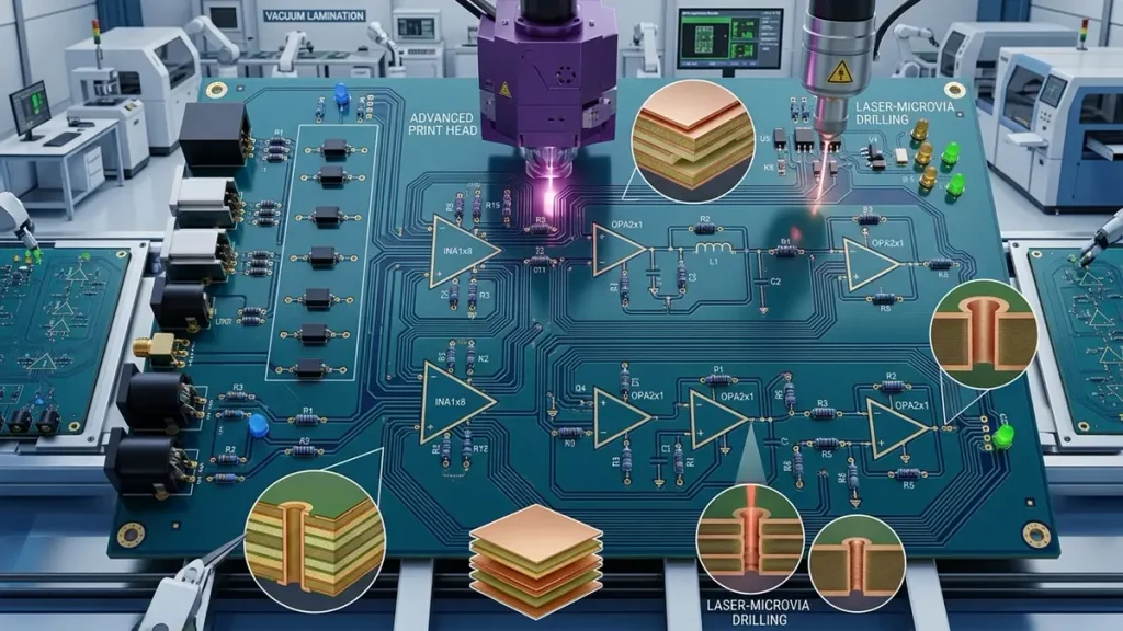
Sensor Signal Filter & Conditioning Board PCB fabrication with fine-line copper traces and laser-drilled microvias
The PCB is not merely a mechanical platform for the circuit. Its layer structure, copper geometry, dielectric properties, via design, registration accuracy, and surface condition can affect signal integrity, grounding, leakage, and assembly reliability.
For a Sensor Signal Filter & Conditioning Board, PCB fabrication should be matched to the electrical requirements and the complexity of the design.
PCB Stackup and Reference Plane Design
A multilayer PCB can provide more controlled routing and reference-plane arrangements than a simple two-layer design.
A four-layer structure may be suitable for many mixed-signal boards, with signal layers and reference planes arranged to support controlled return paths.
A possible stackup may include:
| Layer | Typical function |
|---|---|
| L1 | Sensitive analog signals and selected components |
| L2 | Continuous ground reference plane |
| L3 | Power distribution and selected digital signals |
| L4 | Digital signals and secondary routing |
This is only an example. The final stackup should be based on signal integrity, power distribution, board dimensions, component placement, and manufacturing constraints.
Copper Thickness and Trace Geometry
Copper thickness influences current-carrying capability, resistance, and thermal behavior.
Trace width and spacing affect resistance, parasitic capacitance, coupling, and manufacturing feasibility.
For sensitive analog circuits, predictable trace geometry and routing symmetry can be more important than simply selecting thicker copper.
High-current sensor excitation or power distribution sections may require different copper and thermal design considerations from low-level signal paths.
Precision Imaging and Fine-Line Fabrication
Advanced imaging processes help manufacture fine trace and spacing geometries where dense routing or compact mixed-signal layouts require them.
PCBKR’s manufacturing capability includes SCREEN Ledia LDI imaging, with an 8 µm target and ±10 µm process tolerance as stated capability data. Actual production limits must be evaluated against the selected material, copper thickness, board construction, and finished design requirements.
Fine-line capability is useful when routing density, connector pitch, and component integration require tighter geometries. It should not be confused with a direct guarantee of lower sensor noise.
Multilayer Lamination and Registration
Multilayer lamination quality affects layer bonding, dimensional stability, and interlayer registration.
PCBKR uses LAUFFER lamination equipment with stated pressure settings of 80, 150, and 200 psi and vacuum below 50 mbar.
The appropriate lamination profile depends on the material system, copper distribution, layer count, thickness, and construction requirements.
Consistent registration and lamination help support reliable multilayer routing and via structures.
Laser Drilling and Via Reliability
Laser-drilled microvias may be used in compact, high-density designs where component pitch and routing density justify HDI construction.
PCBKR’s stated laser capabilities include Mitsubishi UV/CO₂ processing at 75 µm ±5 µm and picosecond laser processing at 50 µm.
These capabilities may support more compact interconnections when required by the design. However, many sensor conditioning boards do not need microvias or advanced HDI. A conventional multilayer construction may provide a more economical and robust solution.
Surface Quality, Cleanliness and Insulation
High-impedance analog circuits can be sensitive to leakage and contamination.
Material selection, solder mask design, surface cleanliness, spacing, and assembly process control should be reviewed together.
The fabrication and assembly specification should identify any unusually sensitive nodes, insulation requirements, or cleaning restrictions so the manufacturing team can assess the appropriate process.
Design for Manufacturability Review
A DFM review should examine:
- Stackup and material selection
- Minimum trace width and spacing
- Copper thickness
- Via dimensions and aspect ratio
- Drill-to-copper clearance
- Board thickness and tolerance
- Impedance requirements where applicable
- Surface finish
- Solder mask clearance
- Panelization and tooling
- Sensitive high-impedance areas
The goal is to identify manufacturing risks before production rather than discover them after assembly.
For related manufacturing capabilities, see PCBKR’s HDI PCB manufacturing and microvia PCB information.
9. PCBA Assembly and Testing for Reliable Sensor Conditioning Boards
A well-designed PCB can still fail to achieve its intended performance if component placement, soldering, cleaning, inspection, or electrical testing is inadequate.
Sensor conditioning boards often contain precision analog components whose behavior can be affected by assembly quality and contamination.
SMT and THT Assembly
Surface-mount technology is commonly used for operational amplifiers, ADCs, resistors, capacitors, regulators, and microcontrollers.
Through-hole components may be used for terminal blocks, connectors, large components, or parts requiring mechanical strength.
The assembly process should consider:
- Component package and pitch
- Component orientation
- Polarity-sensitive devices
- Thermal requirements
- Solder paste and reflow profile
- Mixed SMT/THT process sequence
- Mechanical support for connectors
For precision analog boards, the selected component footprint and assembly tolerances should be reviewed before production.
3D AOI and X-Ray Inspection
Automated optical inspection can identify visible assembly defects, including missing components, polarity errors, placement problems, and solder-joint issues within the inspection system’s capabilities.
3D AOI provides additional information about solder-joint geometry and component height.
X-ray inspection is useful for examining hidden solder joints, such as those under BGA packages and other components with inaccessible connections.
These inspection methods improve manufacturing defect detection, but they do not independently verify analog noise, sensor accuracy, ADC linearity, or measurement stability.
Electrical Testing
Electrical testing should be selected according to the board architecture and production requirements.
Possible methods include:
- Flying probe testing
- In-circuit testing where test access and fixtures permit
- Power-on functional testing
- Continuity and short-circuit checks
- Power rail verification
- Communication interface testing
PCBKR’s stated inspection and testing resources include 4-wire Kelvin flying probe testing, 3D AOI, and X-ray inspection.
Four-wire Kelvin measurement can reduce the influence of lead and contact resistance when measuring suitable low-resistance paths. It does not replace complete functional testing of the sensor signal chain.
Functional Testing of Sensor Signal Paths
For a sensor conditioning board, functional validation should use defined electrical input conditions.
A suitable test plan may include:
| Test item | Purpose |
|---|---|
| Input voltage range | Verify the specified sensor input range |
| Gain accuracy | Check amplification against the design target |
| Offset voltage | Evaluate input and output offset |
| Filter response | Confirm the intended frequency response |
| ADC communication | Verify data transfer and interface operation |
| Reference stability | Check reference behavior under defined conditions |
| Channel crosstalk | Evaluate interference between channels |
| Power supply behavior | Verify operating rails and ripple under test conditions |
| Temperature performance | Evaluate drift where required |
| Calibration repeatability | Check consistency across test cycles |
The actual acceptance limits must be defined by the OEM. A manufacturer should not claim a board meets a particular noise or accuracy target without an agreed test method, equipment, input conditions, and documented results.
Calibration and Production Traceability
Some sensor interfaces require gain, offset, or temperature calibration.
Calibration may be performed at board level, system level, or after integration with the sensor, depending on the application.
The RFQ and production specification should define:
- Calibration points
- Reference input conditions
- Measurement equipment
- Acceptance limits
- Calibration data format
- Serial number requirements
- Retest and failure handling procedures
A repeatable production test process helps reduce variation between prototype and volume production.
10. Cost and Lead-Time Factors for Custom Sensor Signal Conditioning Boards
The cost of a custom Sensor Signal Filter & Conditioning Board depends on PCB construction, component selection, assembly complexity, testing requirements, and production quantity.
A low-cost design is not necessarily the most economical solution if it requires repeated engineering changes, difficult calibration, or high production rework.
PCB Fabrication Cost Factors
PCB manufacturing cost is influenced by:
- Board dimensions
- Layer count
- Material selection
- Finished copper thickness
- Board thickness
- Minimum trace width and spacing
- Via structure
- Surface finish
- Impedance requirements
- Special fabrication tolerances
A two-layer board may be sufficient for a relatively simple low-speed sensor interface. A four-layer or higher-layer design may be justified when the board requires controlled reference planes, more complex routing, or greater separation between functional sections.
Advanced HDI should be selected only when the design benefits justify the added manufacturing complexity and cost.
Component and BOM Cost Factors
Precision analog components can contribute significantly to total board cost.
Key cost drivers include:
- Low-noise amplifiers
- Instrumentation amplifiers
- Precision ADCs
- Voltage references
- Precision resistors
- Low-leakage capacitors
- Isolation components
- Protection devices
- Specialized connectors
Component availability and lifecycle status should also be checked before finalizing the BOM.
Where alternatives are permitted, the OEM should define acceptable electrical equivalence criteria rather than allow substitutions based only on package compatibility.
PCBA Complexity and Testing Cost
Assembly cost depends on component count, package type, pitch, SMT/THT mix, assembly side, and process requirements.
Additional cost may come from:
- Fine-pitch components
- BGA assembly
- Manual assembly steps
- Specialized cleaning
- Functional test fixtures
- Calibration equipment
- Serial number and traceability requirements
Testing costs should be evaluated early because precision analog validation may require more than standard continuity and visual inspection.
Prototype, Small-Batch and Mass Production Planning
Prototype production is useful for validating the circuit, layout, and manufacturing process. Small-batch production helps identify repeatability issues before volume manufacturing.
Mass production requires stable documentation, component sourcing, inspection criteria, and production test procedures.
For a more accurate quotation, provide the intended production quantities for prototype, pilot, and recurring orders rather than requesting a quotation based only on a single sample quantity.
11. Manufacturer Selection Criteria for Sensor Signal Conditioning PCB Projects
Selecting a manufacturer for a sensor signal conditioning project requires more than comparing PCB prices.
The supplier should be able to review the PCB design, understand the assembly requirements, identify manufacturing risks, and support the required inspection and testing workflow.
Experience with Mixed-Signal PCB Manufacturing
The supplier should understand the manufacturing considerations of boards combining analog acquisition, digital processing, power management, and communication interfaces.
Relevant review points include:
- Analog and digital layout constraints
- High-impedance input handling
- Multilayer stackup feasibility
- Ground and reference-plane construction
- Component assembly requirements
- Sensitive area cleanliness considerations
Integrated PCB Fabrication and PCBA Assembly
Working with a supplier that supports both PCB fabrication and PCBA assembly can simplify coordination between the bare-board and assembly stages.
It can also make it easier to review material, stackup, component, and assembly requirements together.
For OEMs that need a turnkey or coordinated manufacturing solution, confirm the supplier’s actual sourcing, assembly, inspection, and documentation scope before placing an order.
Quality Control and Inspection Resources
Review the supplier’s inspection process and the relevance of its equipment to the project.
Examples include:
- Optical inspection
- X-ray inspection for suitable packages
- Electrical continuity testing
- Flying probe testing
- Process documentation
- Lot identification and traceability
- Functional test support
The inspection plan should match the board’s risk profile. A generic inspection checklist may not be sufficient for a precision analog product.
Prototype-to-Production Support
A capable supplier should be able to support engineering changes and production scaling without losing control of the manufacturing documentation.
Before selecting a supplier, confirm how it manages:
- Gerber and fabrication data revisions
- BOM changes
- Approved component substitutions
- Assembly drawing updates
- Test specification revisions
- Nonconformance handling
- Production lot records
Technical Communication and RFQ Review
The supplier should identify missing or unclear information before production.
For example, an RFQ that specifies only a board size and quantity may not provide enough information to quote precision analog assembly and functional testing accurately.
A useful technical review should clarify the sensor input range, signal bandwidth, required gain, ADC interface, power architecture, and acceptance criteria.
12. RFQ Requirements for Custom Sensor Signal Filter & Conditioning Boards
A complete RFQ helps the manufacturer evaluate feasibility, material requirements, component sourcing, assembly complexity, and testing scope.
OEM buyers should provide the following information whenever available.
| RFQ information | Recommended details |
|---|---|
| PCB design files | Gerber, ODB++, or approved fabrication data |
| PCB specifications | Layer count, dimensions, thickness, copper weight |
| Stackup | Layer arrangement, dielectric materials, impedance requirements |
| BOM | Part numbers, manufacturers, quantities, approved alternatives |
| Assembly files | Pick-and-place data, assembly drawings, polarity information |
| Sensor type | Voltage, current, thermocouple, RTD, strain gauge, piezoelectric, capacitive, MEMS |
| Input range | Minimum and maximum input voltage or current |
| Signal bandwidth | Required measurement frequency range |
| Amplification | Gain, offset, input impedance, CMRR requirements |
| Filtering | Filter type, cutoff frequency, attenuation requirements |
| ADC interface | ADC model, resolution, sampling rate, input configuration |
| Power requirements | Supply voltage, current, excitation source, reference requirements |
| Isolation | Required isolation voltage and interface details |
| Operating environment | Temperature, humidity, vibration, and other conditions |
| PCBA requirements | SMT/THT, component sourcing, assembly side |
| Testing | Electrical tests, functional tests, calibration, acceptance limits |
| Quantity | Prototype, pilot batch, and recurring production volume |
| Delivery requirements | Target schedule and delivery destination |
If the design is still under development, provide the available schematic, preliminary BOM, sensor datasheet, and system requirements. The manufacturing team can then identify missing production information and potential DFM concerns.
Request a quotation: Send your PCB files, BOM, assembly requirements, and target quantity to sales@pcbkr.com.
13. PCBKR Custom PCB Fabrication and PCBA Assembly Support
Shenzhen Hongda Circuit Technology Co., Ltd. supports OEM customers requiring custom PCB fabrication and PCBA assembly for industrial electronics, embedded control systems, and signal-processing applications.
For Sensor Signal Filter & Conditioning Board projects, manufacturing support can cover bare PCB production, component assembly, inspection, and coordination of production requirements.
PCB Fabrication Capabilities
PCBKR’s stated manufacturing resources include:
- SCREEN Ledia LDI imaging
- Multilayer lamination using LAUFFER equipment
- Mitsubishi UV/CO₂ laser processing
- Picosecond laser processing
- mSAP fine-line manufacturing capability
- Multilayer and HDI PCB production options
The appropriate manufacturing process depends on the actual board design. A conventional multilayer PCB may be sufficient for many sensor conditioning applications, while compact designs may require HDI or finer-line processes.
PCBA Assembly and Inspection
PCBKR provides PCB assembly support for OEM projects requiring SMT and THT processes.
Available inspection and testing resources include:
- 3D AOI
- X-ray inspection
- Four-wire Kelvin flying probe testing
- Electrical inspection according to the agreed production requirements
Functional testing, calibration, and other application-specific validation should be defined in the RFQ and confirmed as part of the project scope.
Prototype, Small-Batch and Volume Production
Different production stages require different levels of engineering and process control.
PCBKR supports prototype, small-batch, and mass-production requirements, subject to design feasibility, component availability, and confirmed production specifications.
Early DFM review can help identify issues involving stackup, component sourcing, assembly access, test points, and manufacturing tolerances before production begins.
Engineering and Quotation Communication
To support a practical quotation, PCBKR encourages OEM customers to provide the PCB design files, BOM, assembly drawings, sensor specifications, and testing requirements.
This allows the manufacturing team to assess the actual production scope rather than estimate cost from board dimensions alone.
Contact PCBKR for custom Sensor Signal Filter & Conditioning Board manufacturing and PCBA assembly.
- Company: Shenzhen Hongda Circuit Technology Co., Ltd.
- Email: sales@pcbkr.com
- Website: www.pcbkr.com
14. Frequently Asked Questions About Sensor Signal Filter & Conditioning Boards
What Is the Difference Between a Sensor Signal Conditioning Board and a Data Acquisition Board?
A sensor signal conditioning board primarily adapts sensor outputs through amplification, filtering, protection, isolation, and signal conversion preparation. A data acquisition board generally includes additional functions for sampling, digitization, data processing, and communication. Some products combine both functions on one PCB.
Which PCB Layer Count Is Suitable for a Low-Noise Sensor Signal Conditioning Board?
A two-layer PCB may be suitable for simple, low-speed sensor interfaces. A four-layer PCB can provide more flexibility for signal routing and continuous reference planes in mixed-signal designs. The final layer count depends on signal sensitivity, channel count, component density, power architecture, and EMI requirements.
Can a PCB Manufacturer Guarantee Low-Noise Sensor Measurement Performance?
PCB manufacturing alone cannot guarantee complete system-level measurement performance. Noise depends on sensor characteristics, amplifier selection, circuit design, layout, power supply, grounding, assembly cleanliness, and test conditions. A manufacturer can support fabrication and assembly consistency, while application-specific noise limits must be verified through defined functional testing.
What Information Is Required for a Sensor Signal Conditioning Board Quotation?
A quotation typically requires Gerber or ODB++ files, PCB specifications, BOM, assembly drawings, sensor input range, signal bandwidth, filtering and amplification requirements, ADC information, production quantity, and testing expectations. More complete technical information helps improve quotation accuracy.
Can PCBKR Support Both PCB Fabrication and PCBA Assembly?
Yes. Shenzhen Hongda Circuit Technology Co., Ltd. provides PCB fabrication and PCBA assembly support for OEM projects. Customers can submit fabrication files, BOM, assembly data, and production requirements to sales@pcbkr.com for technical review and quotation.
What Testing Should Be Specified for a Precision Sensor Conditioning Board?
The test plan should reflect the actual application. Typical requirements may include power rail verification, input range checks, gain and offset measurement, filter response, ADC communication, reference stability, channel crosstalk, and calibration repeatability. Acceptance limits and test conditions should be agreed before production.
Can the Same Sensor Signal Conditioning PCB Be Used for Prototype and Mass Production?
A design can often be transferred from prototype to mass production, but the manufacturing documentation, BOM availability, test fixtures, inspection criteria, and process controls should be reviewed before scaling. A pilot production stage can help identify issues before recurring volume orders.
About Author
David Chen LinkedIn Profile
David Chen is a Senior RF/PCB Process Engineer at Shenzhen Hongda Circuit Technology Co., Ltd., with over 12 years of experience in high-frequency PCB fabrication, impedance-controlled stack-up design, and Rogers/PTFE laminate processing. He also boasts an extensive professional background in PCBA manufacturing, PCBA testing, and PCBA optimization, with specialized expertise in high-precision PCBA fault analysis and rigorous PCBA reliability testing. The author has worked with high-layer-count server PCB fabrication, ultra-low-loss backplane stackups, and thermo-mechanical reliability optimization for AI infrastructure projects involving 112G and 224G PAM4 architectures. Skilled in complex circuit design and cutting-edge advanced PCB manufacturing processes, he delivers solutions that elevate product durability and performance across industrial applications. His technical articles focusing on PCBA manufacturing workflows and testing methodologies are widely cited by industry peers and technical platforms, and have gained attention and recognition from industry colleagues.
Sensor Signal Filter & Conditioning Board – Data Sheet
| Parameter | Specification |
|---|---|
| Product Name | Sensor Signal Filter & Conditioning Board |
| Product Type | Custom Sensor Signal Acquisition and Conditioning PCB |
| Application | Industrial Measurement, Sensor Interfaces, Data Acquisition, Embedded Electronics |
| Sensor Compatibility | Voltage Sensors, Current Sensors, Thermocouples, RTDs, Strain Gauges, Load Cells, Piezoelectric Sensors, Capacitive Sensors, MEMS Sensors |
| Signal Input Types | Single-Ended / Differential |
| Analog Input Range | Customizable according to sensor specifications |
| Current Input | 4–20 mA and other customized ranges |
| Voltage Input | 0–5 V, 0–10 V, and other customized ranges |
| Signal Conditioning | Amplification, Buffering, Level Shifting, Offset Adjustment, Impedance Matching |
| Amplifier Type | Operational Amplifier / Instrumentation Amplifier |
| Filtering Type | Passive RC / Active Low-Pass / High-Pass / Band-Pass / Anti-Aliasing |
| Filter Cutoff Frequency | Customizable according to signal bandwidth |
| Noise Management | Low-Noise Amplification, Power Filtering, Grounding and EMI Control |
| ADC Interface | Single-Ended / Differential, according to ADC selection |
| ADC Resolution | 12-bit / 16-bit / 24-bit or other customized configurations |
| Reference Voltage | Integrated or External Voltage Reference |
| Sensor Excitation | Customized Voltage or Current Excitation |
| Protection Circuit | Overvoltage, ESD, Reverse-Polarity and Input Protection, as required |
| Isolation | Optional Signal or Power Isolation |
| Communication Interface | SPI / I²C / UART / CAN / RS-485, according to system requirements |
| Power Supply | Customized DC Input |
| PCB Material | FR-4 / High-Tg FR-4 / Specialized Materials, according to design |
| PCB Layer Count | 2–20+ Layers, subject to design and manufacturing feasibility |
| PCB Thickness | Customized |
| Copper Thickness | Customized according to current and routing requirements |
| Surface Finish | HASL / Lead-Free HASL / ENIG / Other Available Finishes |
| PCB Technology | Multilayer PCB / HDI PCB / Fine-Line PCB, according to design |
| Assembly Technology | SMT / THT / Mixed Assembly |
| Component Sourcing | Customer-Supplied / Turnkey / Partial Turnkey, subject to project scope |
| Inspection | 3D AOI / X-Ray / Electrical Inspection, according to assembly requirements |
| Electrical Testing | Flying Probe / Continuity / Short-Circuit Testing, as applicable |
| Functional Testing | Optional, according to agreed test specifications |
| Calibration | Optional, according to application requirements |
| Operating Temperature | According to component selection and product design |
| Application Customization | Input Range, Gain, Filter Bandwidth, ADC, Power, Isolation and Interface |
| Production Volume | Prototype / Small Batch / Mass Production |
| Quality Standard | According to agreed IPC requirements and customer specifications |
| Manufacturing Service | Custom PCB Fabrication and PCBA Assembly |
Customization Note: Electrical parameters, sensor compatibility, ADC configuration, filter response, PCB construction, and testing requirements are defined according to the customer’s schematic, BOM, sensor datasheets, and system specifications.
RFQ Contact: sales@pcbkr.com
Manufacturer: Shenzhen Hongda Circuit Technology Co., Ltd.
Website: www.pcbkr.com