High Speed PCB Manufacturing in 2026: Advanced Design, Materials & Signal Integrity Solutions
As data rates push past 112G and 224G thresholds and AI server infrastructure demands ever-tighter tolerances, high speed PCB manufacturing has become one of the most technically demanding disciplines in electronics. At Shenzhen Hongda Circuit Technology Co., Ltd., we engineer and fabricate high-speed printed circuit boards for AI servers, data center switches, 5G base stations, and automotive radar systems — combining rigorous design review, advanced low-loss materials, and precision manufacturing to help our customers achieve signal integrity at the board level.
This guide consolidates everything procurement engineers, hardware designers, and supply chain managers need to evaluate a high-speed PCB supplier in 2026, covering the latest fabrication technology, material science, stackup strategies, and quality benchmarks.
What Is a High Speed PCB? Definitions and Signal Integrity Thresholds for 2026
A printed circuit board is classified as high speed when signal integrity — rather than simple connectivity — becomes the primary design constraint. In practical terms, this threshold is reached when:
- Clock frequencies exceed 100 MHz, or
- Signal rise times fall below 1 nanosecond, or
- Trace lengths approach a significant fraction of the signal’s wavelength
At these conditions, the board stops behaving as a passive conductor and starts acting as a transmission line. Impedance mismatches, dielectric losses, via stubs, and return-path discontinuities all degrade signal quality in measurable ways. An eye diagram that closes, jitter that violates spec, or a channel insertion loss that exceeds budget — these are the failure modes that define high speed PCB design.
By 2026, the practical definition has shifted upward. AI compute boards running NVLink or PCIe Gen 6, data center switches operating at 800G, and 5G massive MIMO front-end modules routinely deal with data rates where FR4 is simply not viable. The high speed category now encompasses virtually all server-class and infrastructure-class hardware.
Key Signal Integrity Parameters Every Buyer Should Know
- Differential impedance control: typically 85Ω or 100Ω ±5% or tighter
- Insertion loss (IL): measured in dB at Nyquist frequency, material-dependent
- Return loss (RL): typically better than -20 dB across the operating band
- Crosstalk (NEXT/FEXT): controlled through trace spacing and layer assignment
- Propagation delay matching: critical for DDR5, SerDes, and multi-lane interfaces
High Speed PCB Design Guidelines: Rules, Stackup, and Layout Best Practices
Strong manufacturing capability means little if the design arriving at the fabricator has not followed high speed PCB design guidelines. At Hongda, our applications engineering team provides pre-production design review as a standard service, catching layout problems before they become costly respins.
Controlled Impedance and Trace Geometry
Every signal layer in a high-speed design must carry controlled-impedance traces. Achieving ±5% impedance tolerance requires precise modeling of trace width, copper thickness after plating, dielectric thickness, and the dielectric constant (Dk) of the laminate — which varies with frequency and temperature. Our fabrication team uses field-solver-calibrated process data, not simplified analytical formulas, ensuring that the impedance delivered on the board matches the simulation model.
Differential Pair Routing Rules
Differential signaling is the backbone of high-speed interfaces from USB to 224G PAM4. Correct differential pair routing requires:
- Matched lengths within 5 mil (or tighter for very high rates) across the pair
- Consistent spacing between the two conductors to maintain coupling
- Symmetric via transitions with matched anti-pads
- Minimized splits and layer changes, each of which introduces impedance discontinuities
Return Path Integrity and Ground Plane Management
The most commonly overlooked aspect of high speed PCB layout is return current management. Every signal current has a return path; at high frequencies that return current flows directly beneath the signal trace on the nearest reference plane. Slots, cutouts, or plane splits that interrupt this path cause emissions and signal degradation. Our design review checklist specifically flags return path violations as a top priority.
Via Stub Elimination Through Back-Drilling
In multilayer PCBs, a through-hole via creates a stub below the last signal layer it connects. At high data rates, this stub acts as a resonant antenna, causing resonant notches in the channel response. Back-drilling — mechanically removing the stub after the board is drilled and plated — is a standard process at Hongda for any design operating above 10 Gbps. Our minimum controlled back-drill depth capability ensures stub lengths below 10 mil.
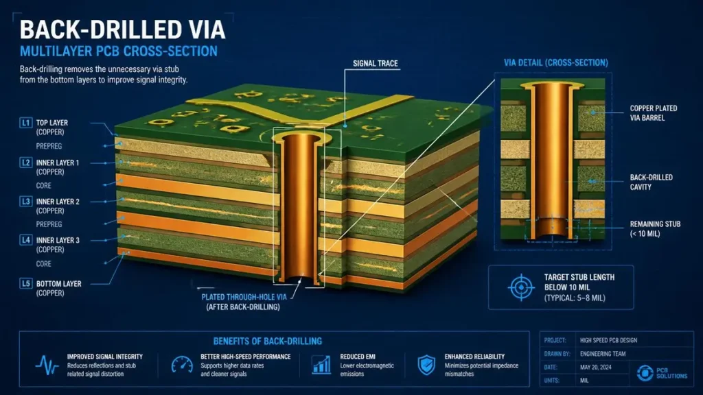
3D cross-section and technical analysis of CNC back-drilling to eliminate unnecessary via stubs.
Length Matching and Skew Control
Multi-lane interfaces such as DDR5, PCIe Gen 5/6, and 400G/800G Ethernet require careful intra-pair and inter-lane length matching. Our CAM tooling performs automated length verification against the design netlist prior to fabrication, providing a match report that becomes part of the board’s quality documentation.
High Speed PCB Materials: Low-Loss Laminates, Rogers vs FR4, and 2026 Material Selection
Material selection is the single most impactful decision in high speed PCB design after topology. The dielectric constant (Dk) and dissipation factor (Df, or loss tangent) of the laminate determine how much signal energy is absorbed by the board as frequency increases. In 2026, the performance gap between commodity FR4 and premium low-loss laminates is wider than ever, because data rates have climbed into territory where FR4’s losses are simply disqualifying. For a detailed head‑to‑head comparison of Megtron 6, Rogers, and Isola laminates – including Dk/Df tables, frequency ranges, and cost trade‑offs – refer to our dedicated material selection guide.
FR4 vs Low-Loss PCB Materials: When to Upgrade
Standard FR4 carries a Dk of approximately 4.2–4.5 and a loss tangent around 0.02 at 1 GHz. For designs operating below 5 Gbps in short channels, FR4 remains a cost-effective choice. For anything above that threshold — particularly for AI server backplanes, high-speed mezzanine cards, or any channel longer than 15 inches — a low-loss material becomes necessary.
Megtron 6 and Megtron 7: The Data Center Standard
Panasonic’s Megtron 6 (Dk ~3.6, Df ~0.004 at 10 GHz) and Megtron 7 (Df ~0.002) have become the de facto materials for data center switch and router PCBs. Hongda is a qualified fabricator for both. The lower dissipation factor directly translates to longer reachable channel lengths and reduced equalization requirements at the SerDes, cutting overall system power consumption.
Rogers Laminates for RF and Microwave Applications
For RF front-ends, antenna feed networks, and millimeter-wave radar boards, Rogers Corporation’s PTFE-based laminates (RO4350B, RO3003, RO4003C) deliver extremely low and stable Dk values from DC to millimeter-wave frequencies. Hybrid stackups combining Rogers signal layers with conventional FR4 core layers are a cost-efficient approach for mixed-signal designs, and Hongda has production experience with this construction.
Isola and Other Alternatives
Isola’s I-Speed and Astra MT77 materials round out the competitive landscape. The right choice depends on channel loss budget, cost constraints, thermal requirements, and whether UL certification for the specific laminate is needed. Our materials engineers will recommend the optimal laminate after reviewing your channel simulation data and mechanical constraints.
PCB Stackup Design for High Speed and AI Server Applications
Stackup design is where signal integrity, power integrity, and manufacturing feasibility intersect. A well-designed stackup controls impedance, manages power distribution, and shields sensitive signal layers from noise sources — all while staying within the fabricator’s layer-count and thickness capabilities. Detailed Guide: Hybrid Stackup PCB (FR4 + Rogers).
Standard High Speed Stackup Configurations
For AI server compute boards and high-speed backplanes, Hongda regularly fabricates stackups in the 12-layer to 32-layer range. A typical 16-layer high-speed stackup for an AI server GPU board uses alternating signal and reference layers, with power planes positioned to maximize inter-plane capacitance for power delivery noise suppression. We provide stackup proposals with impedance tables as part of our pre-production process.
Hybrid Stackups for Mixed-Signal Designs
Designs that combine high-speed digital lanes with analog RF or power stages benefit from hybrid stackups that isolate these domains. Placement of ground planes between digital and analog sections provides electromagnetic shielding, reducing coupling. Our applications team works with customers to define layer assignments that optimize both signal integrity and manufacturability.
Power Integrity Integration
In 2026, power integrity (PI) and signal integrity (SI) are treated as joint problems, not separate disciplines. Simultaneous switching noise from AI accelerators can couple onto signal traces and degrade the eye diagram. Our team’s pre-production review includes PI analysis for critical power domains, recommending decoupling capacitor placement, via fanout strategies, and plane cavity resonance mitigation.
High Speed PCB Manufacturing Technology: Hongda’s 2026 Fabrication Capabilities
High speed PCB manufacturing requires tighter process control than standard fabrication across every step, from inner-layer imaging to final electrical test. Our Shenzhen facility has invested continuously in process capability since our founding, building a production infrastructure capable of meeting the demands of the most complex AI and data center boards in the market.
Layer Count and Registration Precision
Hongda produces multilayer PCBs from 2 to 40 layers. For high-layer-count boards, layer-to-layer registration directly affects impedance repeatability and via reliability. We use laser drilling for microvias and X-ray-verified registration at each lamination cycle to maintain copper pad-to-via alignment within ±50 μm.
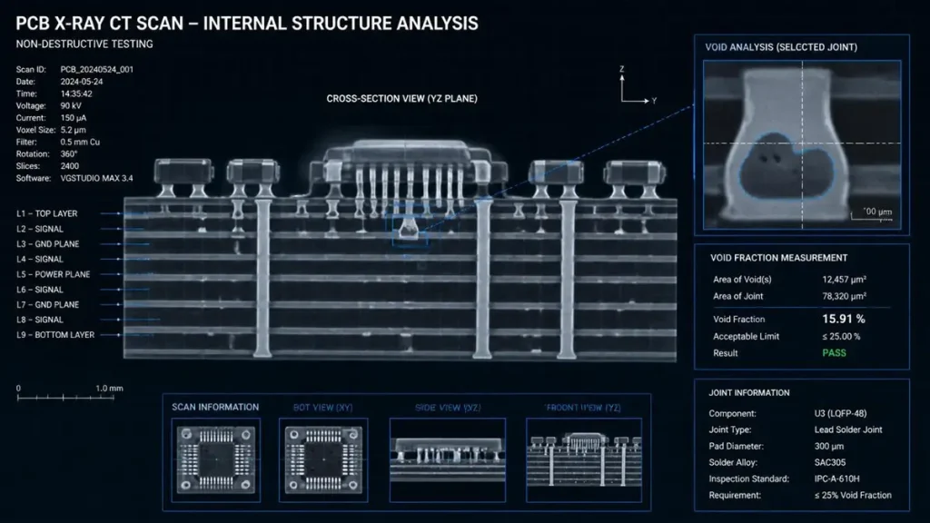
Hongda PCB X-Ray Structure Analysis
HDI PCB Manufacturing for AI and High-Density Interconnect
High-density interconnect (HDI) construction enables finer pitch BGA escape routing and reduced stub lengths. Our HDI capabilities include any-layer via structures, stacked and staggered microvias, and via-in-pad with planarization — all required for leading-edge processor and memory packaging on AI compute boards.
Back-Drilling for Stub Elimination
As mentioned in the design section, back-drilling is a critical process for channels above 10 Gbps. Our CNC back-drilling process delivers controlled depth accuracy of ±75 μm, with in-process measurement to verify stub removal before subsequent processing steps.
Impedance Controlled PCB Manufacturing
Every impedance-controlled production lot at Hongda includes coupon-based TDR (time-domain reflectometry) measurement of all specified impedance structures. Test coupons are fabricated on the same panel as the production boards, ensuring the measurement reflects actual process conditions. Results are reported on a per-lot basis and included in the shipment documentation.
Advanced Surface Finishes
Surface finish selection affects both solderability and high-frequency performance. We offer ENIG, ENEPIG, hard gold, immersion silver, and OSP. For high-frequency applications, immersion silver provides excellent RF performance at lower cost than ENEPIG, and our controlled silver thickness process minimizes the risk of silver migration in humid environments.
Signal Integrity Testing and PCB Validation Methods
Manufacturing to specification is only half the job. Verification that the finished board meets its electrical requirements requires systematic testing infrastructure, and Hongda invests in the measurement equipment needed to verify high-speed performance at production scale.
TDR Impedance Testing
Time-domain reflectometry is our primary tool for impedance verification. Every production lot of impedance-controlled boards receives TDR testing on representative coupons. The measurement records are retained and available for customer review. For critical applications, we also offer full-board TDR mapping upon request.
VNA-Based S-Parameter Measurement
For RF and microwave designs, vector network analyzer (VNA) measurements provide the full frequency-domain characterization that TDR does not. We perform S-parameter measurement for antenna boards, RF coupler circuits, and any design where insertion loss or return loss must be verified to a specified frequency.
Flying Probe and Fixture-Based Electrical Test
All production boards receive 100% electrical test for continuity and isolation. For high-volume production, we use fixture-based in-circuit testing for throughput efficiency. For prototype and low-volume runs, flying probe testing eliminates the fixture lead time and cost, enabling faster prototype cycles.
High Speed PCB Applications: AI Servers, Data Centers, 5G, and Automotive
The applications driving high speed PCB demand in 2026 share a common thread: they all require moving data faster than previous generations, with less tolerance for signal degradation and less power budget to compensate for board-level losses.
AI Server PCB Design and GPU Board Fabrication
AI accelerator boards for training and inference workloads represent the most demanding segment of the PCB market. GPU-to-GPU interconnects such as NVLink operate at data rates that require sub-millimeter trace width control, precisely back-drilled vias, and ultra-low-loss laminates. Hongda has production experience with these boards and understands the unique challenges of their thermal management and mechanical constraints.
Data Center Switch and Router PCBs
400G and 800G Ethernet switches require backplanes and line cards with channel performance that was considered exceptional just five years ago. High-layer-count boards with tight impedance control, Megtron 6 or equivalent laminates, and verified S-parameter performance are standard expectations. Our data center customer base has pushed our process capabilities to levels that directly benefit other markets.
5G Infrastructure PCB Manufacturing
5G base station and Massive MIMO antenna array PCBs combine digital baseband processing with RF front-end functions on the same board or closely coupled assemblies. The combination of fine-pitch BGA packages, high-frequency RF traces, and thermal management requirements makes 5G PCBs among the most multi-disciplinary products we fabricate.
Automotive Radar and ADAS PCBs
Millimeter-wave radar for autonomous driving and ADAS operates at 77 GHz and above, requiring PTFE-based laminates with extremely low and consistent Dk. The automotive supply chain also imposes IATF 16949 process standards, traceability requirements, and AEC-Q200 component compatibility checks that demand mature manufacturing systems. Hongda supports automotive customers with full production traceability and supports PPAP documentation.
Why Choose Shenzhen Hongda Circuit Technology Co., Ltd. as Your PCB Manufacturing Partner
Procurement managers evaluating high-speed PCB suppliers in 2026 face a market where technical claims are easy to make and difficult to verify. Hongda differentiates through documented process capability, engineering support depth, and a track record across the most demanding applications in the industry.
Technical Capabilities at a Glance
- Layer count: 2 to 40 layers, including HDI any-layer constructions
- Minimum line width/spacing: 2.5 mil / 2.5 mil
- Controlled impedance tolerance: ±5%, with ±3% available on request
- Back-drilling depth accuracy: ±75 μm
- Materials: FR4, Megtron 6/7, Rogers RO4350B/RO3003, Isola I-Speed, PTFE hybrid
- Surface finishes: ENIG, ENEPIG, hard gold, immersion silver, OSP
- Electrical test: 100% flying probe and fixture-based testing
- Certifications: ISO 9001, UL, IPC-6012 Class 3
Engineering Support Throughout the Project Lifecycle
From stackup co-design and DFM review before the first Gerber is submitted, through first article inspection and production qualification, Hongda’s engineering team works as an extension of your hardware development organization. We do not simply receive files and run production; we engage at the design stage to prevent problems that would otherwise surface during prototype bring-up.
Responsive Delivery for Prototype and Production
Prototype PCB cycles as fast as 24–48 hours for standard constructions, and accelerated production for HDI and high-layer-count boards are available. Our production planning team provides committed delivery dates at order confirmation, with proactive communication if anything changes.
FAQs
What certifications should a high speed PCB manufacturer hold to qualify as a serious supplier for AI and data center applications?
At minimum, look for ISO 9001 quality management certification and UL recognition for the specific materials and constructions you require. For AI server and data center applications, IPC-6012 Class 3 compliance — which imposes tighter acceptance criteria than Class 2 — is a meaningful differentiator. For automotive applications, IATF 16949 certification is typically a hard requirement. Ask suppliers for their current UL file number and request a copy of their most recent quality audit summary. Shenzhen Hongda Circuit Technology Co., Ltd. holds ISO 9001 certification and IPC-6012 Class 3 process qualification, with UL recognition for standard and halogen-free FR4, Megtron 6, and select Rogers laminates.
How do I evaluate a PCB manufacturer’s impedance control capability before placing an order?
Request sample TDR test reports from recent production lots for structures comparable to your design requirements. A credible supplier will have coupon-based impedance data on file and will share it without hesitation. Ask specifically whether they use coupon-based measurement (preferred, as it reflects actual board conditions) or model-based calculation only. Also verify that their process capability study covers the material and construction you intend to use — impedance capability on FR4 does not automatically transfer to Megtron 6 or Rogers. At Hongda, every impedance-controlled lot generates TDR records that are retained for a minimum of three years and available for customer review.
What is the difference between high speed PCB manufacturing and standard PCB fabrication, and does it cost significantly more?
High speed PCB manufacturing involves tighter process controls at nearly every step: more precise inner-layer imaging to hold fine line widths, more careful lamination to achieve tight dielectric thickness tolerances, back-drilling operations absent from standard boards, 100% TDR or VNA verification that standard boards do not require, and premium laminates that carry a material cost premium over commodity FR4. The total cost premium over standard fabrication ranges from 20% to several times the base cost, depending on layer count, material selection, and the specific process steps required. However, the relevant comparison is not high-speed versus standard board cost — it is the cost of a working board versus the cost of a field failure or a respin caused by signal integrity problems on a cheaper board. For AI server and infrastructure applications, using a qualified high-speed PCB manufacturer is a risk management decision, not just a technical one.
How should I compare PCB supplier quotes for high speed boards to make sure I’m making a true apples-to-apples comparison?
Request that each supplier quote against an identical specification document that includes: material by brand and grade (not just “low-loss material”), impedance structures and target values with tolerance, back-drill requirements (depth, diameter, count), surface finish and minimum gold or silver thickness where applicable, IPC acceptance class, electrical test method and coverage, and required test documentation. Differences in any of these parameters will invalidate a direct price comparison. Common areas where low-priced quotes conceal higher risk include substituting a lower-grade laminate, omitting back-drilling, quoting IPC Class 2 instead of Class 3, and providing model-based impedance “verification” instead of coupon TDR measurement.
What lead times should I expect for prototype and production high speed PCBs from a supplier in Shenzhen, and how can I reduce them?
For standard high-speed PCB constructions using FR4 or Megtron 6 up to 16 layers without HDI, prototype lead times of 5–7 working days are typical from Shenzhen, with expedited 2–3 day service available at a premium. HDI constructions, back-drilling, and layer counts above 20 layers typically add 3–5 working days. Production volumes generally carry lead times of 2–4 weeks depending on capacity. Lead times can be reduced by submitting complete Gerber packages with fully defined impedance and back-drill requirements on the first submission, avoiding the back-and-forth of incomplete data clarification. Establishing a qualified supplier relationship before production ramp-up — rather than qualifying a new supplier under schedule pressure — is the most reliable way to protect delivery timelines.
Ready to discuss your high speed PCB project?
Contact the engineering team at Shenzhen Hongda Circuit Technology Co., Ltd. for a free design review and quotation. Our applications engineers will review your stackup, impedance requirements, material selection, and back-drill specification, and respond with a detailed technical and commercial proposal within 24 hours.
About Author
David Chen https://www.linkedin.com/in/pcbcoming
David Chen boasts an extensive professional background in PCBA manufacturing, PCBA testing, and PCBA optimization, with specialized expertise in high-precision PCBA fault analysis and rigorous PCBA reliability testing. The author has worked with high-layer-count server PCB fabrication, ultra-low-loss backplane stackups, and thermo-mechanical reliability optimization for AI infrastructure projects involving 112G and 224G PAM4 architectures. Skilled in complex circuit design and cutting-edge advanced PCB manufacturing processes, he delivers solutions that elevate product durability and performance across industrial applications. His technical articles focusing on PCBA manufacturing workflows and testing methodologies are widely cited by industry peers, research institutions, and technical platforms, solidifying his reputation as a recognized technical authority in the global circuit board manufacturing sector.