Does RF PCB Design Require High-Speed Techniques?
For years, RF PCB design and high-speed digital design were treated as two separate disciplines, handled by different engineers, governed by different rulebooks, and often laid out on different boards entirely. That separation no longer holds.
In millimeter-wave radar modules, 5G base station front-ends, and the early 6G prototypes now moving through development labs, RF circuitry and high-speed digital interfaces sit on the same substrate, share the same ground system, and influence each other’s performance in ways that single-discipline design rules cannot address.
So the question PCB buyers, RF engineers, and procurement teams keep asking is a fair one: does RF PCB design actually require high-speed techniques, or is this just industry buzz? Based on current millimeter-wave radar and 5G/6G manufacturing practice, the answer is unambiguous: yes. Once RF and high-speed digital circuits coexist on the same board, high-speed design discipline — signal integrity management, impedance control, return path planning, crosstalk suppression, and EMI containment — becomes mandatory, not optional. This article, prepared by the engineering team at Shenzhen Hongda Circuit Technology Co., Ltd., walks through why that is the case, how isolation is achieved in mixed RF/high-speed boards, and what it takes to manufacture these boards reliably in 2026.
RF PCB Design and High-Speed Techniques: Why the Two Disciplines Have Merged
The Short Answer: RF PCB Design Requires High-Speed Design Thinking
When an RF PCB carries only analog RF circuitry — a single antenna feed, a simple matching network, nothing else — traditional RF layout rules are often sufficient. That scenario is increasingly rare. Modern RF PCB design usually places a radio front-end alongside PCIe lanes, DDR memory interfaces, SerDes links, or high-speed ADC/DAC data paths on the same stack-up. The moment those elements share a board, RF performance becomes a function of how well the high-speed digital domain is controlled. Reflections from poorly terminated digital traces, ground bounce from switching power delivery, and electromagnetic coupling from dense digital routing all leak into the RF domain unless high-speed techniques are applied from the first layout pass.
Why RF and High-Speed Digital Signals Now Share the Same Board
Three market forces are driving this convergence. First, millimeter-wave radar systems for automotive and industrial sensing need to process gigahertz-level RF returns and then immediately digitize, process, and transmit that data over high-speed digital buses — all within a compact module. Second, 5G and emerging 6G radio units integrate RF transceivers directly next to baseband processors and high-speed memory, eliminating the cable runs and separate boards that used to isolate these domains. Third, board real estate and cost pressure push designers toward consolidated, multi-domain PCBs rather than multi-board assemblies connected by RF cabling. The result is that RF PCB design is no longer a standalone exercise — it is one layer of a high-speed, mixed-signal system design problem.
Isolation Design Strategies for RF and High-Speed Coexistence
Once RF and high-speed digital circuits are forced to share a board, the design challenge shifts from “how do I route this signal” to “how do I keep these domains from interfering with each other.” Four techniques form the backbone of practical RF/high-speed isolation design.
Zone Partitioning in RF PCB Layout
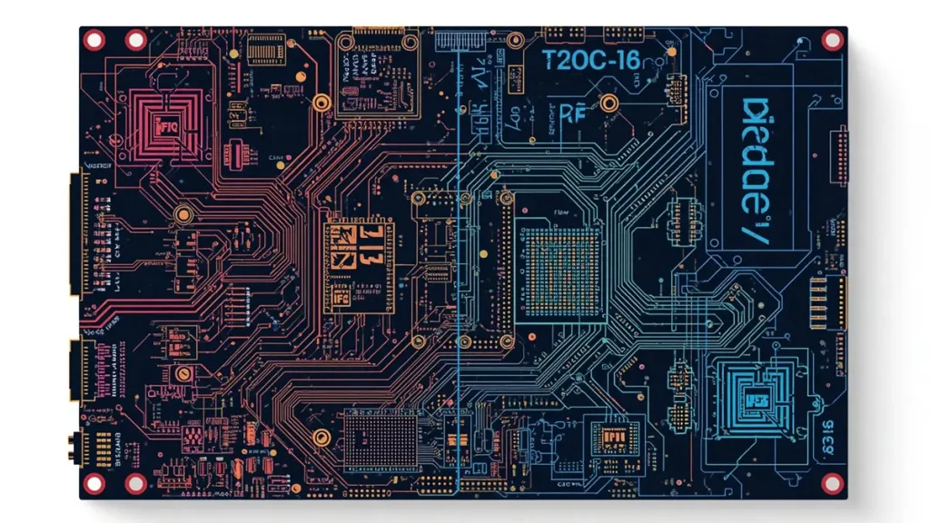
RF and Digital Zone Partitioning in Mixed-Signal PCB Layout
Physical separation remains the first line of defense. RF sections, high-speed digital sections, and sensitive analog circuitry are grouped into distinct zones on the board, with RF components placed as far as practical from noisy digital switching circuits and clock sources. Careful zone planning also dictates connector placement and cable routing, since even a well-isolated RF zone can be compromised by a high-speed cable running directly above it.
Ground and Power Plane Isolation for High-Speed RF Circuits
Shared, noisy ground returns are one of the most common sources of RF degradation on mixed-signal boards. High-speed RF PCB design typically calls for segmented ground and power planes — separating digital return currents from RF return currents — combined with controlled stitching points that prevent ground loops while still maintaining a low-impedance reference for both domains. Power plane partitioning, paired with targeted decoupling, keeps switching noise from digital regulators and high-speed I/O out of sensitive RF supply rails.
Shielding and Via Fencing Around Sensitive RF Traces
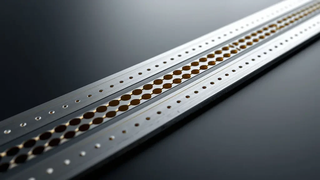
3D Close-up of RF Trace with Grounded Via Fence
Grounded via fences, also called via stitching walls, are placed along the edges of sensitive RF transmission lines to contain electromagnetic fields and block coupling from adjacent high-speed traces. In denser designs, localized shielding cans or conformal shielding are added over RF sections to further suppress radiated coupling from nearby digital circuitry — a technique borrowed directly from high-speed EMI containment practice and applied to RF protection.
Return Path Control Across RF and High-Speed Domains
Both RF signals and high-speed digital signals depend on a continuous, low-impedance return path directly beneath the signal trace. Any gap in the reference plane — a slot, a via field, a layer transition without a stitching via — forces return current to detour, creating radiated emissions and crosstalk that can degrade RF performance just as easily as it can break a high-speed digital eye diagram. Disciplined return path management, a core high-speed design technique, is just as critical on the RF side of a mixed board.
Millimeter-Wave Radar PCB Design: Where RF Precision Meets High-Speed Discipline
Millimeter-wave radar boards represent one of the clearest cases where RF PCB design cannot be separated from high-speed technique.
Material Selection for Millimeter-Wave RF PCB Manufacturing
At millimeter-wave frequencies, dielectric loss and material consistency have an outsized effect on signal quality. Low-loss, tightly controlled laminates are required for the RF layers, while the digital layers on the same stack-up may use more cost-effective, standard materials — meaning the stack-up itself has to be engineered as a hybrid structure rather than a single uniform material set.
Trace Geometry and Impedance Control in Radar PCB Design
RF traces on millimeter-wave boards need to be short, straight, and dimensionally precise, since any corner, width variation, or via transition introduces impedance discontinuities that show up as reflections and insertion loss. Antenna feed lines and matching networks must also be physically separated from nearby high-speed digital routing, since even modest electromagnetic coupling at these frequencies can distort radar return signals and reduce detection accuracy.
5G/6G PCB Design: High-Speed Techniques as a Core RF Requirement
RF Front-End and High-Speed Digital Interface Coexistence in 5G/6G PCB Design
5G radio units and emerging 6G prototypes routinely place RF transceivers on the same board as PCIe, DDR, and other high-speed digital interfaces. In these designs, high-speed routing rules — controlled trace length matching, differential pair routing, via optimization — directly determine whether the RF front-end can meet its noise and linearity targets. There is no longer a meaningful line between “the RF section” and “the high-speed section” of these boards; they are designed as one interdependent system.
6G RF PCB Design and the Growing Isolation Challenge
As development moves toward 6G frequency bands, channel bandwidths widen and carrier frequencies climb further into the millimeter-wave and sub-terahertz range. Every increase in frequency tightens the tolerance on layer stack-up, trace width and spacing, and impedance consistency, and makes RF-to-digital isolation progressively harder to achieve. Boards designed for 6G prototyping already require high-speed design rigor that exceeds what most 5G-era RF PCBs needed.
RF PCB Manufacturing Challenges in High-Speed, High-Frequency Designs
Design rules only matter if a manufacturer can actually build the board to spec. Mixed RF/high-speed boards introduce manufacturing challenges that go well beyond standard PCB fabrication.
Material Selection Trade-offs in RF PCB Manufacturing
Combining low-loss RF laminates with standard digital materials in a single stack-up requires careful management of lamination compatibility, coefficient of thermal expansion mismatches, and bonding process parameters — challenges that simply do not exist on single-material boards.
Processing Precision for High-Frequency, High-Speed PCB Fabrication
Millimeter-wave and high-speed digital circuits are far more sensitive to fabrication tolerances than legacy RF boards. Trace width and spacing, via wall quality, and edge chamfering all need tighter process control, since deviations that would be invisible on a low-frequency board translate directly into measurable RF performance loss or signal integrity failures at gigahertz speeds.
Stack-Up Complexity in Mixed RF and Digital PCB Manufacturing
A single board now has to satisfy RF layer requirements, high-speed digital layer requirements, and isolated power/ground structures simultaneously. Stack-up design and lamination process control become significantly more complex than on a conventional multilayer board, and manufacturing engineering has to be involved early in the design cycle rather than after layout is finished.
Testing and Validation of High-Speed RF PCBs
Verifying that an RF and high-speed mixed-signal board actually meets its targets requires a combination of full-wave simulation, time-domain reflectometry (TDR) for impedance verification, and vector network analysis for RF performance — testing methods drawn from both the RF world and the high-speed digital world, applied together.
How Shenzhen Hongda Circuit Technology Supports RF and High-Speed PCB Manufacturing in 2026
As an RF PCB manufacturer working directly with customers in radar, 5G/6G communications, and high-speed mixed-signal applications, Shenzhen Hongda Circuit Technology Co., Ltd. has aligned its 2026 manufacturing capability around exactly the challenges described above. This includes hybrid stack-up lamination for boards combining low-loss RF laminates with standard FR-4 or high-speed digital materials, fine-line mSAP (modified semi-additive process) capability for tighter trace width and spacing control, laser-drilled microvia formation for HDI structures used in compact radar and 5G/6G modules, and automated optical inspection combined with TDR-based impedance verification on every high-speed/RF production run. The goal is straightforward: give engineering teams a manufacturing partner that already understands why RF PCB design requires high-speed techniques, instead of one that treats RF and high-speed as separate, disconnected production lines.
Conclusion: RF PCB Design Is a High-Speed, High-Frequency, and Manufacturing Integration Problem
The original question — does RF PCB design require high-speed techniques — has a clear answer once millimeter-wave radar and 5G/6G applications are considered. RF design can no longer be evaluated in isolation. The real engineering challenge sits at the intersection of RF performance, high-speed digital signal integrity, and manufacturing precision: isolation strategy, impedance control, and fabrication tolerance all have to be solved together, on the same board, at the same time. As frequencies climb toward 6G and module density keeps increasing, this need for combined RF and high-speed design discipline will only grow stronger, and the manufacturers who can execute on both fronts will be the ones buyers turn to for these projects.
Frequently Asked Questions
How do I find an RF PCB manufacturer that also understands high-speed design rules?
Look for a manufacturer that can show direct experience with mixed RF and high-speed digital boards — not just RF boards and high-speed boards as separate product lines. Ask for stack-up examples, impedance test reports (TDR data), and references from radar or 5G/6G customers specifically, since these applications require both disciplines applied together.
What questions should I ask a supplier about millimeter-wave PCB manufacturing capability?
Ask about minimum trace width and spacing they can hold in production, their experience laminating low-loss RF materials together with standard digital materials in one stack-up, their laser-drilling and microvia capability, and what RF test data (insertion loss, return loss) they provide as standard with each production batch.
How do I evaluate a PCB manufacturer’s experience with RF and high-speed coexistence on the same board?
Request example projects or case studies involving RF front-ends paired with PCIe, DDR, or other high-speed interfaces on a single board, and ask how they handled ground plane partitioning, shielding, and return path continuity in those designs. A manufacturer with real experience will be able to discuss these details specifically rather than in general terms.
What certifications or quality processes matter most when sourcing high-speed RF PCBs?
Beyond standard quality certifications (ISO 9001, IATF 16949 for automotive radar applications), confirm the supplier performs impedance verification via TDR on every relevant production lot, has automated optical inspection in place for fine-line processes, and can supply test coupons and electrical test reports alongside the finished boards.
How do I compare quotes from different RF PCB suppliers when the boards involve both RF and high-speed sections?
Compare quotes based on the full stack-up specification, not just layer count and board thickness — confirm which layers carry RF material versus digital material, what impedance tolerances are guaranteed, and whether RF and high-speed testing is included in the quoted price or billed separately, since these factors affect both cost and the reliability of the final board.
Shenzhen Hongda Circuit Technology Co., Ltd.
RF and high-speed PCB manufacturer specializing in millimeter-wave radar, 5G/6G communication, and mixed RF/digital boards, with 2026 manufacturing capability covering hybrid stack-up lamination, fine-line mSAP processing, laser-drilled microvias, and TDR-based impedance verification.
About Author
David Chen https://www.linkedin.com/in/pcbcoming
David Chen boasts an extensive professional background in PCBA manufacturing, PCBA testing, and PCBA optimization, with specialized expertise in high-precision PCBA fault analysis and rigorous PCBA reliability testing. The author has worked with high-layer-count server PCB fabrication, ultra-low-loss backplane stackups, and thermo-mechanical reliability optimization for AI infrastructure projects involving 112G and 224G PAM4 architectures. Skilled in complex circuit design and cutting-edge advanced PCB manufacturing processes, he delivers solutions that elevate product durability and performance across industrial applications. His technical articles focusing on PCBA manufacturing workflows and testing methodologies are widely cited by industry peers, research institutions, and technical platforms, solidifying his reputation as a recognized technical authority in the global circuit board manufacturing sector.