Gold Finger PCB Cost & Buying Guide: Prices, MOQ, Lead Times & Supplier Selection
Gold Finger PCB Cost Quick Summary: Gold finger PCBs remain the gold standard for edge connectors in high-insertion applications. In 2026, selective hard gold plating, precision beveling, and advanced nickel barrier technologies continue to dominate the landscape. This guide breaks down real pricing factors, lead time realities, and what separates a reliable gold finger PCB manufacturer from a risky one — with actionable insights from Shenzhen Hongda Circuit Technology Co., Ltd. , a China-based specialist serving 60+ countries.
1. What Is a Gold Finger PCB and Why Does It Matter?
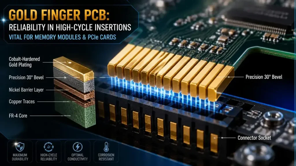
Gold Finger PCB Structure & Hard Gold Plating Cross-Section Guide
A gold finger PCB refers to a printed circuit board with gold-plated contact pads along one edge, designed to slide into a mating connector or slot. These edge connectors — commonly called PCB gold fingers or gold finger edge connectors — provide the electrical bridge between your board and the outside world.
Unlike standard surface finishes such as HASL or OSP, gold finger plating must survive repeated insertion cycles without degradation. That is why the industry relies on selective hard gold plating rather than immersion finishes like ENIG. Hard gold contains cobalt or nickel alloys that increase surface hardness to 130–200 HV, whereas ENIG remains too soft for mechanical wear applications.
The most common applications include:
- Memory modules (DDR4, DDR5, DIMM)
- Graphics cards and PCIe expansion cards
- Industrial control boards with hot-swappable interfaces
- Network interface cards and server backplanes
- Test fixtures and burn-in boards
In 2026, demand for high-reliability gold finger PCBs has surged alongside AI server builds and edge-computing hardware, where connector integrity directly impacts system uptime.
2. How Much Does a Gold Finger PCB Cost? (2026 Price Benchmarks)
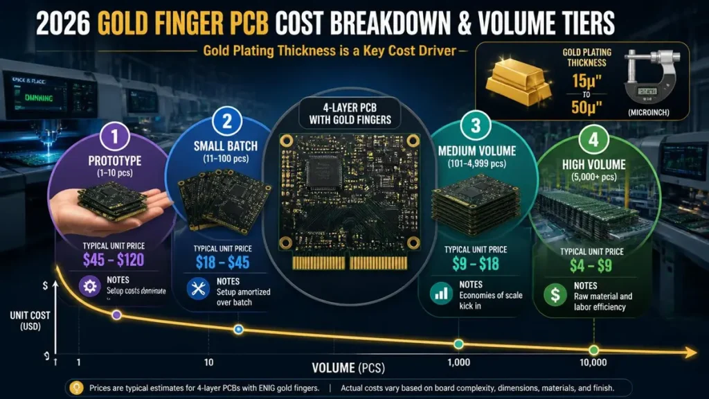
Gold Finger PCB Cost Breakdown & Tiered Pricing Benchmark (2026)
2.1 Prototype vs. Mass Production Pricing
Gold finger PCB cost follows a tiered structure. For a standard 4-layer FR-4 board with selective hard gold on edge connectors:
| Volume Tier | Typical Unit Price | Notes |
|---|---|---|
| Prototype (1–10 pcs) | $45–$120 per board | Setup and plating bar costs dominate |
| Small batch (50–200 pcs) | $18–$35 per board | Economy of scale begins |
| Medium volume (500–2,000 pcs) | $8–$16 per board | Tooling amortized |
| High volume (5,000+ pcs) | $4–$9 per board | Raw material and labor efficiency |
These figures assume 30 µ” (0.75 µm) hard gold thickness over 3–5 µm electroplated nickel. Thicker gold — such as 50 µ” (1.25 µm) for military-grade connectors — can add 25–40% to the plating cost.
2.2 MOQ Policies: What Buyers Actually Face
Most gold finger PCB manufacturers enforce a minimum order quantity (MOQ) driven by plating line setup rather than board fabrication. The selective plating process requires:
- A dedicated plating bar (busbar) design
- Masking film or photoresist application
- Separate electrolytic bath cycles
At Shenzhen Hongda Circuit Technology Co., Ltd., we operate a flexible MOQ model. For standard gold finger prototypes, we accept orders starting at 5 pieces without punitive surcharges. This is possible because our HX automated plating line handles quick changeovers between hard gold and standard surface finishes, reducing setup waste.
For buyers evaluating gold finger PCB suppliers, ask specifically whether the MOQ applies to the total panel count or the unique part number. Some factories quote low MOQs but require 20+ panels per run, effectively forcing higher volume commitments.
3. Key Factors Influencing Gold Finger PCB Price
3.1 Plating Type: Hard Gold vs. ENIG vs. ENEPIG
This is the single largest cost driver. Here is how the three primary finishes compare for edge connector applications:
| Finish | Hardness | Gold Thickness | Insertion Cycles | Relative Cost | Best For |
|---|---|---|---|---|---|
| Electroplated Hard Gold | 130–200 HV | 0.5–2.0 µm | 1,000+ | Highest | Gold fingers, edge connectors, test points |
| ENIG | 60–90 HV | 0.05–0.15 µm | <10 | Lowest | Solderable pads, not for wear |
| ENEPIG | 90–110 HV | 0.08–0.20 µm | 50–100 | Medium | Wire bonding + moderate insertion |
Hard gold PCB plating remains the only viable choice for connectors requiring >500 insertion cycles. ENIG fails rapidly under mechanical friction. ENEPIG has gained traction for mixed-use boards where some pads need wire bonding and others see occasional insertion, but it still cannot replace hard gold for high-cycle edge connectors.
At PShenzhen Hongda Circuit Technology Co., Ltd., we plate hard gold per MIL-DTL-45204 with cobalt-hardened electrolyte. Our XRF (X-Ray Fluorescence) verification ensures gold thickness uniformity within ±10% across the finger array.
3.2 Gold Thickness: 5 µ” to 50 µ” and Beyond
Gold thickness for PCB edge connectors typically ranges from 5 microinches (0.13 µm) to 50 microinches (1.27 µm). The selection depends on insertion frequency and environmental exposure:
- 5–10 µ” (0.13–0.25 µm): Low-cycle consumer electronics, <100 insertions
- 15–30 µ” (0.38–0.76 µm): Standard industrial and computing applications, 500–1,000 insertions
- 50 µ” (1.27 µm): Military, aerospace, and high-reliability test fixtures, >5,000 insertions
Thicker gold increases material cost linearly — gold accounts for roughly 60% of the plating process cost at 50 µ”. However, spec’ing 50 µ” for a consumer product is economic overkill. A competent gold finger PCB manufacturer should advise you on the minimum thickness required for your insertion cycle target.
3.3 Board Specifications: Layers, Thickness, and Material
Gold finger PCBs are not limited to simple 2-layer or 4-layer designs. In 2026, we see increasing demand for:
- High-layer-count gold finger boards (12–24 layers) for server backplanes
- High-TG FR-4 (TG170–TG180) for thermal stability during reflow
- Hybrid stack-ups with Rogers or Taconic materials near RF sections
Each additional layer adds lamination cycles, which increases cost by 8–15% per pair of layers. For boards with gold fingers on both edges or internal connector slots, routing and plating complexity rises further.
3.4 Beveling Angle and Edge Tolerance Control
PCB gold finger beveling — cutting the board edge at an angle (typically 20°, 30°, or 45°) — is mandatory for smooth connector insertion. In 2026, automated CNC beveling machines have replaced manual grinding in top-tier facilities, achieving:
- Angle tolerance: ±1° (vs. ±3° for manual)
- Bevel depth consistency: ±0.1 mm
- Surface roughness: Ra <0.8 µm
Standard gold finger bevel angles:
- 30°: Industry default for PCIe, DIMM, and most card-edge connectors
- 45°: High-density connectors where reduced insertion force is critical
- 20°: Specialized industrial backplanes
Poor beveling causes connector damage and gold peeling. At Shenzhen Hongda Circuit Technology Co., Ltd., we use precision grinding equipment followed by 100% optical inspection of the beveled edge before final electrical test.
4. Lead Times and Turnaround: How Fast Can You Get Gold Finger PCBs?
4.1 Standard Lead Times by Volume
| Production Stage | Standard Lead Time | Expedited Lead Time |
|---|---|---|
| Prototype (1–20 pcs) | 5–7 days | 48–72 hours |
| Small batch (50–500 pcs) | 10–12 days | 5–7 days |
| Mass production (1,000+ pcs) | 15–20 days | 10–12 days |
The plating process adds 1–2 days to standard PCB fabrication because hard gold requires:
- Solder mask application on the full board
- Selective masking to expose only finger areas
- Nickel strike and gold electrolytic deposition
- Mask stripping and edge beveling
4.2 Expedited Gold Finger PCB Manufacturing
Fast-turn gold finger PCB prototyping is achievable when the factory maintains dedicated plating capacity rather than outsourcing. At Shenzhen Hongda Circuit Technology Co., Ltd., our in-house HX automated plating line and SCREEN Ledia LDI exposure system allow us to process prototype gold finger orders within 48 hours for standard 4-layer designs.
The key constraint on expedited lead time is not plating itself — it is the DFM review and plating bar design. A poorly designed plating bar (the temporary conductive connection used during electrolysis) can cause uneven gold distribution. We complete this engineering review within 1 hour of Gerber submission, preventing delays.
5. How to Choose a Gold Finger PCB Manufacturer: 2026 Evaluation Framework
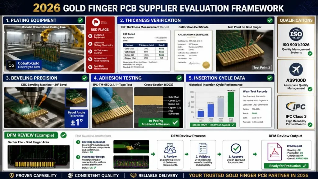
2026 Gold Finger PCB Supplier Technical Evaluation Framework
5.1 Technical Capability Checklist
Not every PCB factory can reliably produce gold finger boards. Use this gold finger PCB supplier evaluation checklist:
| Evaluation Dimension | What to Verify | Red Flags |
|---|---|---|
| Plating Equipment | Dedicated electrolytic hard gold line with cobalt-nickel bath | Outsourced plating; no in-house bath chemistry control |
| Thickness Verification | XRF (X-Ray Fluorescence) measurement with calibration certificates | Manual eddy-current gauges only; no traceable reports |
| Beveling Precision | CNC beveling with ±1° angle tolerance | Hand-ground edges; no angle inspection |
| Adhesion Testing | Tape test per IPC-TM-650 2.4.28; cross-section analysis | No adhesion data; refusal to provide micro-sections |
| Insertion Cycle Data | Historical test data for comparable applications | No wear-test records; vague “high reliability” claims |
| Layer Count Support | Capability up to your required layer count | Maximum 4-layer capability for complex designs |
5.2 Quality Certifications That Matter
For gold finger PCB procurement, prioritize suppliers with:
- ISO 9001:2015 (minimum baseline)
- IPC-6012 Class 3 or 3A (high-reliability structural integrity)
- IPC-A-600 (acceptability of printed boards)
- AS9100D (for aerospace-grade gold finger applications)
- IATF 16949 (automotive connector applications)
Shenzhen Hongda Circuit Technology Co., Ltd. holds ISO 9001:2026, AS9100D, and IPC-6012 Class 3/3A certifications. Our quality framework extends to 100% 3D X-Ray (AXI) inspection and AI-driven process monitoring, ensuring that even traditional gold finger boards benefit from chip-level precision.
5.3 Engineering Support and DFM Review
The best gold finger PCB suppliers distinguish themselves before production begins. A thorough DFM review for gold finger designs should cover:
- Edge keep-out zones: Traces and vias must stay ≥1.0 mm from the beveled edge to prevent copper exposure
- Plating bar routing: The temporary conductive path must not interfere with final board functionality
- Solder mask clearance: 0.5 mm minimum clearance from gold finger pads
- Impedance continuity: For high-speed edge connectors (PCIe, NVMe), TDR verification at the finger interface
At Shenzhen Hongda Circuit Technology Co., Ltd., our engineering team reviews every gold finger RFQ within 1 hour. We flag plating bar conflicts, beveling interference, and impedance discontinuities before quoting — not after you have placed the order.
6. RFQ Checklist: What to Include in Your Gold Finger PCB Inquiry
A complete gold finger PCB RFQ prevents quoting delays and manufacturing errors. Include these items:
6.1 Gerber and Design Files
- Gerber RS-274X with clear outline layer
- Mechanical layer specifying bevel angle, depth, and location
- Layer stack-up with controlled impedance requirements
- Drill file (Excellon) with plating specifications
6.2 Critical Parameters to Specify
| Parameter | Typical Specification | Why It Matters |
|---|---|---|
| Gold thickness | 30 µ” (0.76 µm) over 3–5 µm nickel | Determines insertion cycle life |
| Gold alloy | Cobalt-hardened per MIL-DTL-45204 | Wear resistance and hardness |
| Bevel angle | 30° ±2° | Connector compatibility |
| Bevel depth | 1.0 mm ±0.2 mm | Insertion smoothness |
| Surface finish (rest of board) | ENIG, OSP, or HASL | Solderability of component pads |
| Plating bar removal | Yes, with flush cut | Prevents electrical shorts |
6.3 What Happens During a 24-Hour Engineering Review
When you submit a complete RFQ to Shenzhen Hongda Circuit Technology Co., Ltd., our review process covers:
- DFM validation: Beveling clearance, trace-to-edge spacing, plating bar feasibility
- Stack-up verification: Impedance simulation for high-speed gold finger interfaces
- Material compatibility: Confirming laminate choice supports hard gold adhesion
- Cost optimization: Recommending gold thickness and beveling specs that meet your reliability target without over-engineering
Gold Finger PCB FAQ:
What is the difference between hard gold and ENIG for PCB gold fingers?
Hard gold is electroplated, alloyed with cobalt or nickel for hardness (130–200 HV), and deposited at 0.5–2.0 µm thickness. It survives 1,000+ insertion cycles. ENIG is an immersion process depositing a thin, soft gold layer (0.05–0.15 µm) that is solderable but wears out in under 10 insertions. For edge connectors, hard gold is mandatory; ENIG is only suitable for solderable pads.
Why are gold finger PCBs more expensive than standard PCBs?
Three factors drive the premium: (1) Selective plating requires masking, a separate electrolytic bath, and dedicated tooling; (2) Gold material cost — even at 30 µ”, gold contributes 15–25% of the plating process cost; (3) Beveling and inspection add machining and metrology steps. The plating bar design and XRF thickness verification are non-standard processes that standard PCB lines do not perform.
What gold thickness is recommended for standard PCIe and edge connectors?
For consumer and industrial PCIe cards, 30 µ” (0.76 µm) hard gold over 3–5 µm nickel is the industry standard. This supports 500–1,000 insertion cycles. For test fixtures and burn-in boards subject to daily insertion, 50 µ” (1.27 µm) is recommended. Military specifications often require 50 µ” minimum with cobalt-hardened alloy per MIL-DTL-45204.
Can I order small-batch gold finger PCB prototypes without high MOQ fees?
Yes — if you select a manufacturer with flexible plating line setup. At Shenzhen Hongda Circuit Technology Co., Ltd., we accept gold finger prototype orders starting at 5 pieces. Our automated plating line handles quick changeovers, eliminating the traditional MOQ penalty that comes from dedicated bath preparation. The key is submitting complete Gerber files with beveling specifications to avoid engineering delays.
How do I verify a gold finger PCB manufacturer can actually deliver reliable boards?
Request four pieces of evidence: (1) XRF thickness reports from recent production lots showing gold uniformity; (2) Cross-section photomicrographs of nickel and gold layers; (3) Adhesion test results per IPC-TM-650; and (4) Beveling angle inspection data with tolerance verification. If a supplier cannot provide these, they likely lack process control. Certifications (ISO 9001, IPC-6012 Class 3) are necessary but not sufficient — demand production data.
Ready to Source Your Gold Finger PCBs? Start Here
Gold finger PCB procurement does not need to be opaque. With clear specifications, a verified supplier checklist, and realistic lead time expectations, you can eliminate the hidden costs and quality risks that plague edge connector projects.
Shenzhen Hongda Circuit Technology Co., Ltd. manufactures gold finger PCBs from prototype to mass production, with in-house hard gold plating, precision beveling, and IPC Class 3 quality systems. Our 2026 equipment lineup — including SCREEN Ledia LDI, Mitsubishi laser drilling, and Nordson DAGE X-Ray inspection — delivers the precision that high-reliability connectors demand.
Next Step: Upload your Gerber files, stack-up, and beveling specifications to sales@pcbkr.com. Our engineering team will return a DFM review and detailed quotation within 24 hours.
Company: Shenzhen Hongda Circuit Technology Co., Ltd.
Website:www.pcbkr.com
Email:sales@pcbkr.com
Phone: +86 0755 23720053
Certifications: ISO 9001:2026 | AS9100D | IPC-6012 Class 3/3A | ISO 13485
Headquarters: Room 1608-1610, Research Development Comprehensive Building, Baoyunda Logistics Center, Baoan, Shenzhen, China
About Author
David Chen https://www.linkedin.com/in/pcbcoming
David Chen boasts an extensive professional background in PCBA manufacturing, PCBA testing, and PCBA optimization, with specialized expertise in high-precision PCBA fault analysis and rigorous PCBA reliability testing. The author has worked with high-layer-count server PCB fabrication, ultra-low-loss backplane stackups, and thermo-mechanical reliability optimization for AI infrastructure projects involving 112G and 224G PAM4 architectures. Skilled in complex circuit design and cutting-edge advanced PCB manufacturing processes, he delivers solutions that elevate product durability and performance across industrial applications. His technical articles focusing on PCBA manufacturing workflows and testing methodologies are widely cited by industry peers, research institutions, and technical platforms, solidifying his reputation as a recognized technical authority in the global circuit board manufacturing sector.