Glass Epoxy PCB Manufacturer for Custom PCB Production
When you need a reliable glass epoxy PCB manufacturer, the key decision is not simply whether a supplier can fabricate FR-4. Your supplier must control laminate selection, glass-resin construction, multilayer registration, drilling, lamination, copper plating, surface finish, inspection, and production consistency. Shenzhen Hongda Circuit Technology provides custom glass epoxy PCB manufacturing for prototypes, multilayer boards, HDI structures, and production programs.
Request a Glass Epoxy PCB Quote
Why Choose a Glass Epoxy PCB Manufacturer Based on Manufacturing Capability?
A glass epoxy PCB supplier should be evaluated by its ability to convert your design requirements into a stable production process.
For procurement teams, the important question is not:
“Can you make an FR-4 PCB?”
The more useful question is:
“Can you manufacture this specific glass epoxy PCB construction repeatedly within the required dimensional, electrical, thermal, and quality tolerances?”
That distinction becomes important when a board moves beyond a simple two-layer design.
A custom glass epoxy PCB may require:
- Multiple copper layers
- Controlled dielectric thickness
- Tight layer-to-layer registration
- Fine-pitch BGA routing
- Blind or buried vias
- Laser-drilled microvias
- Controlled impedance
- High-Tg FR-4
- Low-loss glass-epoxy laminates
- Heavy copper
- ENIG, OSP, HASL or other surface finishes
- AOI and X-Ray inspection
- Electrical testing
- Microsection analysis
- Prototype-to-production process transfer
For this reason, supplier selection should begin with manufacturing-process compatibility, not only unit price.
What Does a Glass Epoxy PCB Manufacturer Actually Control?
The finished PCB is the result of several interacting variables rather than one material specification.
For a glass epoxy PCB, the manufacturing chain can be viewed as:
Laminate → Glass/Resin Construction → Circuit Geometry → Lamination → Drilling → Plating → Surface Finish → Inspection → Electrical Test → Shipment
Each stage can influence the final board.
Glass epoxy laminate selection
The laminate supplier and exact material grade should be identified in the RFQ.
Depending on the application, engineers may select:
- Standard FR-4
- High-Tg FR-4
- Halogen-free FR-4
- Low-loss FR-4
- High-speed glass-epoxy materials
- Application-specific laminate systems
A material should not be selected solely from the word “FR-4.” The actual datasheet values, construction, glass style, resin content, dielectric properties, thermal characteristics, and applicable standards should be reviewed.
Glass-resin construction
Glass cloth provides reinforcement, while the resin system fills the spaces between glass bundles and contributes to the dielectric and thermal behavior of the laminate.
This makes prepreg selection particularly important in multilayer fabrication.
The manufacturer needs to match:
- Glass style
- Resin content
- Press thickness
- Copper distribution
- Finished dielectric thickness
- Lamination conditions
- Required impedance
Poor material matching can create thickness variation, registration problems, resin starvation, or inconsistent electrical performance.
How Does Glass Epoxy PCB Fabrication Control Multilayer Registration?
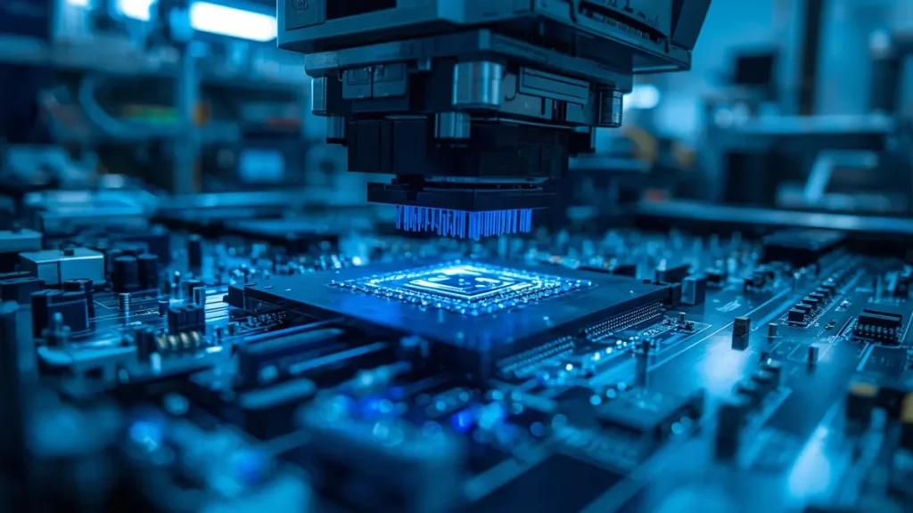
Multilayer PCB Registration and Alignment Testing
For multilayer glass epoxy PCB production, layer registration is one of the most important manufacturing variables.
A multilayer board is constructed from several materials with different thermal expansion behavior. During lamination, heating and cooling cause dimensional movement.
If that movement is not properly compensated, the consequences may include:
- Via-to-pad misalignment
- Reduced annular ring
- Via breakout
- BGA pad connection risk
- Registration-related yield loss
- Difficulty meeting fine-line requirements
How does a manufacturer reduce registration risk?
A controlled manufacturing process can use:
- Material-specific compensation
- Symmetrical stackup construction
- Controlled lamination
- Panel distortion measurement
- LDI imaging
- Layer registration verification
- Pre-production engineering review
The important procurement question is therefore not simply whether the supplier owns an LDI machine.
Ask the supplier:
How is layer distortion measured, compensated, and verified during production?
That question reveals substantially more about manufacturing maturity.
How Do LDI and Advanced Imaging Improve Glass Epoxy PCB Production?
Laser Direct Imaging (LDI) transfers the circuit pattern directly onto the photoresist rather than depending entirely on conventional phototool alignment.
For a custom glass epoxy PCB, this can be particularly valuable when the design includes:
- Fine line/space
- High-density routing
- Small pads
- Fine-pitch BGA escape
- HDI structures
- Tight registration requirements
The advantage is not simply higher imaging resolution.
The real manufacturing value comes from combining imaging precision with:
Panel measurement → Image compensation → Pattern exposure → Registration verification
This process-oriented approach helps reduce the accumulation of dimensional errors across multilayer production.
For procurement, LDI capability should therefore be evaluated together with the supplier’s actual design rules and inspection methodology.
How Does mSAP Affect Fine-Line Glass Epoxy PCB Manufacturing?
When conventional subtractive etching becomes a limiting factor for very fine geometries, Modified Semi-Additive Processing (mSAP) can provide another manufacturing route.
In an mSAP process, copper is selectively built up and patterned to achieve fine conductor geometries.
This technology is useful for glass epoxy PCB designs requiring:
- Fine line/space
- High-density interconnects
- Fine-pitch BGA routing
- Compact multilayer layouts
- Shorter electrical paths
- Higher routing density
However, mSAP should not be treated as a universal replacement for conventional PCB fabrication.
The correct process depends on:
- Required line/space
- Copper thickness
- Layer construction
- Pad geometry
- Via architecture
- Production volume
- Yield target
- Cost target
A professional glass epoxy PCB manufacturer should determine whether conventional subtractive processing, semi-additive processing, or mSAP is appropriate for the actual design.
How Does Lamination Affect Glass Epoxy PCB Reliability?
Lamination is one of the most important stages in multilayer glass epoxy PCB fabrication because it transforms individual cores, prepregs, and copper foils into a mechanically integrated multilayer structure.
The engineering objective is not merely to bond layers together.
The process must achieve:
- Uniform dielectric thickness
- Reliable resin flow
- Strong interlayer bonding
- Controlled registration
- Low void risk
- Stable board thickness
- Controlled thermal stress
What can go wrong during lamination?
Several common manufacturing problems are associated with poor process control:
Resin starvation
Insufficient resin flow can leave areas around copper structures without adequate resin coverage.
Voids
Entrapped air or inadequate lamination conditions can create internal voids.
Layer misregistration
Material movement during pressing can shift circuit layers relative to one another.
Warpage
Asymmetric copper distribution or an unbalanced construction can increase board deformation.
Delamination
Poor bonding, contamination, excessive thermal stress, or unsuitable material/process combinations can create interlayer separation.
For demanding multilayer boards, the supplier should be able to explain how the stackup is translated into a validated lamination process.
How Does Drilling Affect Glass Epoxy PCB Quality?
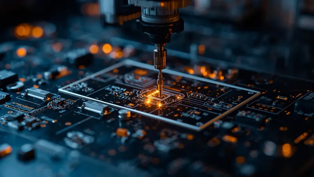
Glass Epoxy PCB CNC Drilling Process
Drilling is another area where the glass reinforcement of FR-4 creates a different machining environment from softer PCB materials.
The drill passes through a composite structure containing:
Copper + epoxy resin + woven glass reinforcement + copper
These materials do not respond identically to mechanical or laser processing.
A manufacturing process therefore needs to control:
- Drill diameter
- Hole positional accuracy
- Drill depth
- Tool wear
- Hole wall condition
- Burr formation
- Resin smear
- Glass/resin interface quality
What about laser drilling?
Laser drilling is particularly useful for HDI glass epoxy PCBs.
Depending on the construction and approved process, laser processing can create:
- Blind microvias
- Small-diameter interconnects
- Sequential HDI structures
- Via-in-pad structures
- Fine interconnect features
The engineering target should never be described only as “smallest hole diameter.”
A more useful specification is:
Diameter + depth + positional accuracy + taper + copper interface + plating reliability
That gives both engineering and procurement teams a meaningful basis for supplier qualification.
How Does Desmear and Copper Plating Affect Glass Epoxy PCB Reliability?
After drilling, the hole structure needs appropriate preparation before copper metallization.
Drilling can leave resin smear and affect the condition of the hole wall.
An effective desmear process prepares the surface for reliable copper deposition.
The subsequent metallization sequence generally includes:
Hole preparation → Electroless copper → Electrolytic copper → Pattern plating / outer-layer processing
Copper plating quality directly affects interconnection reliability.
Critical factors include:
- Copper thickness
- Plating uniformity
- Hole-wall coverage
- Via integrity
- Surface preparation
- Current distribution
- Aspect ratio
- Thermal reliability
For multilayer boards, a visually perfect external surface does not necessarily prove that the internal interconnections are reliable.
That is why cross-section analysis and appropriate electrical/reliability testing can be important for qualified production.
Which Glass Epoxy PCB Manufacturing Technologies Matter Most in 2026?
The direction of PCB manufacturing in 2026 is toward higher density, tighter dimensional control, automated inspection, and better process traceability.
For glass epoxy PCB production, the technologies with the greatest practical impact include:
Laser Direct Imaging
Used to improve pattern transfer and registration control for dense circuitry.
Laser drilling
Supports HDI and microvia structures where conventional mechanical drilling is insufficient.
mSAP
Provides an advanced route for fine conductor geometries.
Controlled vacuum lamination
Helps manage resin flow, trapped air, dielectric thickness, and multilayer bonding.
Automated optical inspection
AOI identifies many external pattern and solder-mask-related defects before shipment.
X-Ray inspection
X-Ray provides visibility into selected internal structures that cannot be confirmed through surface inspection alone.
Microsection analysis
Cross-sectioning allows engineers to examine:
- Copper thickness
- Hole-wall quality
- Via structure
- Registration
- Dielectric construction
- Plating interfaces
The key trend is therefore process integration, rather than purchasing one “advanced” machine.
A capable glass epoxy PCB manufacturer should connect equipment, process parameters, inspection, and engineering feedback into one manufacturing system.
How Does Shenzhen Hongda Circuit Approach Custom Glass Epoxy PCB Manufacturing?
At Shenzhen Hongda Circuit Technology Co., Ltd., custom glass epoxy PCB production is approached as a manufacturing-engineering problem.
Our process begins with the customer’s actual requirements and works backward to determine the appropriate manufacturing route.
The engineering review can consider:
Material → Stackup → Circuit Geometry → Via Structure → Lamination → Drilling → Plating → Surface Finish → Testing
This approach is particularly useful when a board contains multiple manufacturing constraints.
Engineering review before production
A pre-production review can identify potential risks involving:
- Minimum trace/space
- Pad-to-via relationships
- Annular ring
- Layer registration
- Board thickness
- Copper distribution
- Drill-to-copper clearance
- HDI structures
- Controlled impedance
- Surface finish
- Panel utilization
The purpose is straightforward:
Identify manufacturing risk before it becomes production yield loss.
What Glass Epoxy PCB Capabilities Should Buyers Verify?
A supplier’s capability table should be compared with the actual design requirements.
Important qualification categories include:
| Requirement | What to Verify |
|---|---|
| Laminate | Manufacturer and exact material grade |
| Glass epoxy construction | Core/prepreg structure and resin system |
| Layer count | Standard and advanced production range |
| Board thickness | Available finished thickness |
| Copper | Inner and outer copper capability |
| Line/space | Minimum production geometry |
| Drilling | Mechanical and laser capability |
| Microvias | Diameter, depth and structure |
| HDI | Blind/buried and sequential structures |
| Registration | Production tolerance and measurement method |
| Lamination | Process control and stackup compatibility |
| Surface finish | ENIG, HASL, OSP and other approved finishes |
| Inspection | AOI, X-Ray and microsection |
| Electrical test | Flying probe or fixture testing |
| Engineering | DFM and stackup review |
| Production | Prototype, pilot and volume capability |
This qualification method prevents a common sourcing mistake: selecting a supplier based on a broad “FR-4 PCB” claim without verifying the actual construction required by the project.
How Can a Glass Epoxy PCB Supplier Reduce Your Procurement Risk?
The lowest quotation is not necessarily the lowest total cost.
For PCB procurement, the real cost of an unreliable manufacturing process can include:
- Prototype delays
- Engineering revisions
- Scrap
- Rework
- Assembly problems
- Field failures
- Qualification delays
- Production interruptions
- Expedited logistics
A more useful supplier evaluation model is:
Unit Price + Yield + Quality Risk + Lead Time + Engineering Support + Supply Stability
What evidence should a supplier provide?
Before approving a supplier, buyers can request:
- Material datasheets
- Manufacturing capability information
- DFM feedback
- Stackup proposal
- Cross-section examples
- Inspection records
- Electrical test methodology
- Reliability documentation where applicable
- First-article documentation
- Traceability information
A supplier that can explain how a requirement will be manufactured and verified is generally more useful than one that simply promises that the requirement can be met.
Can a Glass Epoxy PCB Manufacturer Support Prototypes and Mass Production?
Yes, but prototype capability and production capability should be evaluated separately.
A supplier may successfully manufacture a small prototype while having difficulty maintaining the same process window at production volume.
For this reason, buyers should ask how the supplier handles:
Prototype
The objective is rapid technical validation.
Typical engineering priorities include:
- DFM review
- Material confirmation
- Stackup verification
- First article inspection
- Electrical testing
- Cross-section validation when required
Pilot production
The objective is to verify process stability.
Important indicators include:
- Repeatability
- Registration consistency
- Plating consistency
- Yield
- Inspection results
- Process documentation
Mass production
The objective becomes stable, repeatable supply.
Procurement teams should evaluate:
- Capacity
- Production scheduling
- Material availability
- Process control
- Traceability
- Quality consistency
- Change-control procedures
This prototype-to-production transition is especially important for multilayer glass epoxy PCB programs.
What Applications Are Suitable for Custom Glass Epoxy PCBs?
Glass epoxy PCBs are used across a wide range of electronic products because they provide a practical combination of mechanical structure, electrical insulation, thermal resistance, and manufacturability.
Typical applications include:
- Industrial control systems
- Automotive electronics
- Medical electronics
- Telecom equipment
- Networking equipment
- Power electronics
- Instrumentation
- Consumer electronics
- Embedded control systems
- High-density digital equipment
The exact laminate and construction should be selected according to the application’s electrical, thermal, mechanical, and reliability requirements.
For example, a basic industrial controller may require a very different glass epoxy PCB construction from a high-density networking board.
What Should You Include in a Glass Epoxy PCB RFQ?
A complete RFQ helps a manufacturer quote accurately and reduces engineering clarification cycles.
Include:
PCB construction
- Layer count
- Board dimensions
- Finished thickness
- Copper thickness
- Laminate grade
- Core/prepreg information
- Surface finish
Circuit requirements
- Minimum trace/space
- Minimum drill
- Via types
- Microvia dimensions
- Annular ring
- BGA pitch
- Controlled impedance requirements
Manufacturing requirements
- IPC class
- Dimensional tolerance
- Solder-mask requirements
- Silkscreen
- Copper requirements
- Panelization preference, if applicable
Testing requirements
- Electrical test
- AOI
- X-Ray
- Microsection
- Impedance testing
- Reliability testing, where required
Commercial information
- Prototype quantity
- Pilot quantity
- Mass-production quantity
- Required delivery date
- Packaging requirements
- Destination
For the fastest technical evaluation, provide Gerber, ODB++, IPC-2581, drill data, fabrication drawings, and the intended stackup whenever available.
How Do You Request a Glass Epoxy PCB Quote from Shenzhen Hongda Circuit?
A useful RFQ should allow our engineers to evaluate both technical feasibility and manufacturing economics before production begins.
Send your available PCB design data together with:
- Quantity
- Board dimensions
- Layer count
- Material preference
- Thickness
- Copper weight
- Surface finish
- Special via requirements
- Impedance requirements
- Testing requirements
- Target delivery schedule
Our engineering review can then determine the appropriate fabrication route and identify potential DFM issues before quotation.
For complex multilayer, HDI, fine-line, or high-reliability glass epoxy PCB projects, this early engineering review can be more valuable than simply comparing several unit-price quotations.
Glass Epoxy PCB Manufacturer FAQ
What should I look for in a glass epoxy PCB manufacturer?
Look beyond the supplier’s material list. Verify its ability to manufacture your actual layer count, board thickness, copper weight, line/space, drilling structure, registration requirement, surface finish, and testing specification.
For complex boards, request evidence such as DFM feedback, sample cross-sections, inspection records, and material documentation.
Can Shenzhen Hongda manufacture custom glass epoxy PCBs?
Yes. Shenzhen Hongda Circuit Technology provides custom PCB fabrication using FR-4 and related glass-epoxy material systems, with engineering review and manufacturing processes selected according to the approved design.
For unusual constructions or advanced requirements, capability should be confirmed during engineering review before production commitment.
Can a glass epoxy PCB manufacturer produce multilayer and HDI boards?
Yes, multilayer glass epoxy PCBs can be manufactured using sequential lamination, controlled drilling, microvia processing, and high-density circuit fabrication where the design is compatible with the supplier’s validated process capability.
The correct HDI structure should be confirmed from the actual stackup and design files rather than inferred from the layer count alone.
What files are needed for a glass epoxy PCB quotation?
The preferred RFQ package includes Gerber or ODB++ files, drill files, fabrication drawings, stackup information, board dimensions, copper thickness, material requirements, surface finish, impedance requirements, quantity, and testing specifications.
Providing complete fabrication information allows the manufacturer to identify DFM risks and produce a more reliable quotation.
How can I compare glass epoxy PCB suppliers?
Compare suppliers using the same technical RFQ and evaluate five areas together:
Manufacturing capability + quality evidence + engineering support + lead-time reliability + total cost.
Do not compare unit prices until the suppliers have confirmed that they are quoting the same material, construction, process, testing, and quality requirements.
Request a Glass Epoxy PCB Quote
Your glass epoxy PCB should be evaluated as a complete manufacturing system—not simply as an FR-4 material selection.
Shenzhen Hongda Circuit Technology Co., Ltd. can support custom PCB projects from engineering review through fabrication and production.
If you have a new glass epoxy PCB, FR4 glass epoxy PCB, multilayer PCB, or HDI design, send your fabrication data for engineering evaluation.
Request a Glass Epoxy PCB Quote
Website: www.pcbkr.com
Email: pcb@pcbkr.com
Recommended RFQ Information
Board Type: Glass Epoxy / FR-4
Layers:
Board Size:
Thickness:
Copper Weight:
Minimum Line/Space:
Via Structure:
Surface Finish:
Quantity:
Required Delivery:
Our engineering team can review your requirements and identify the appropriate manufacturing route before production.
About Author
David Chen https://www.linkedin.com/in/pcbcoming
David Chen boasts an extensive professional background in PCBA manufacturing, PCBA testing, and PCBA optimization, with specialized expertise in high-precision PCBA fault analysis and rigorous PCBA reliability testing. The author has worked with high-layer-count server PCB fabrication, ultra-low-loss backplane stackups, and thermo-mechanical reliability optimization for AI infrastructure projects involving 112G and 224G PAM4 architectures. Skilled in complex circuit design and cutting-edge advanced PCB manufacturing processes, he delivers solutions that elevate product durability and performance across industrial applications. His technical articles focusing on PCBA manufacturing workflows and testing methodologies are widely cited by industry peers, research institutions, and technical platforms, solidifying his reputation as a recognized technical authority in the global circuit board manufacturing sector.