Copper Base PCB Manufacturing Process: How 2026 Fabrication Technology and Advanced Equipment Shape BoardQuality
Metal-core boards do not fail the same way FR-4 boards fail. When a copper base PCB goes
wrong, it is almost always at one of six points in the process: cutting, lamination, drilling,
etching, surface finish, or testing. Buyers sourcing a copper base PCB manufacturer rarely
ask about these points directly, but they are exactly what separates a board that survives
100,000 thermal cycles from one that delaminates in the field. This article walks through
the copper base PCB manufacturing process step by step, explains why metal substrate
fabrication diverges from conventional PCB production, and shows how the equipment on
our floor at Shenzhen Hongda Circuit Technology Co., Ltd. (PCBKR) supports both
prototype runs and volume orders.
What Is a Copper Base PCB and Why Manufacturers Specify It
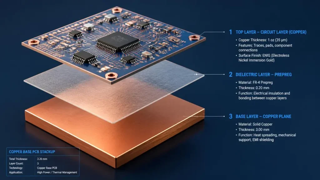
Copper Base PCB Stackup and Layer Structure
A copper base PCB uses a solid copper plate as its structural and thermal layer instead of
the woven glass-epoxy core found in standard FR-4 laminate. A thin dielectric layer bonds
the copper core to the circuit layer above it, giving the board a thermal conductivity that FR
4 cannot approach. Designers reach for copper base construction — sometimes labeled
copper-clad or copper substrate PCB — when a board has to move heat away from power
devices faster than an aluminum-backed board allows: high-power LED arrays, power
converters, motor drivers, and increasingly, 800V EV traction electronics.
The trade-off is manufacturability. Copper is denser and more thermally conductive than
aluminum, which changes drilling speed, etch chemistry behavior, and lamination pressure
profiles. A shop that runs standard aluminum PCB tooling without adjustment will produce
copper base boards with rough hole walls, uneven line width, or warped panels.
Copper Base PCB Manufacturing Process: Step-by-Step Flow From Material Cutting to Final Test
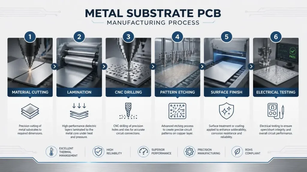
6-Step Metal Substrate PCB Manufacturing Process Timeline
The production sequence follows six core stages: material cutting, lamination, drilling,
etching, surface finish, and testing. Each stage carries different risk on a metal-core panel
than it does on a glass-epoxy panel.
Material Cutting and Dimensional Control for Metal Substrate Board
The copper plate arrives to size tolerance and flatness requirements tighter than FR-4 sheet
stock. Edge quality matters more here than on standard laminate — a cracked or burred
edge on a copper core propagates into delamination during later thermal cycling. Cutting
parameters are set to hold panel dimension and squareness before the panel ever reaches
lamination, since any correction attempted later in the line is far more expensive.
Lamination: Bonding Copper Core to Dielectric Layer
This is the step that decides whether a copper base board holds together for its rated life.
Temperature, pressure, and dwell time have to be matched to the specific dielectric — thin,
thermally-conductive prepreg behaves differently under heat than standard FR-4 prepreg,
and getting the profile wrong produces trapped air, uneven bond-line thickness, or bow and
twist across the panel. High-end lamination presses with tight platen temperature
uniformity and programmable pressure ramps are what make this repeatable at volume
rather than dependent on operator feel.
Drilling Copper Core Material: Hole Position and Wall Quality
Drilling a solid copper substrate is mechanically closer to metalworking than to standard
PCB drilling. Copper is more ductile than the fiberglass-resin matrix in FR-4, so a drill bit
and feed rate tuned for FR-4 will smear or burr the hole wall instead of cutting it cleanly,
and can also shorten bit life dramatically. Hole position accuracy and wall roughness both
need dedicated process parameters for metal substrate drilling, and this is one of the two or
three points buyers should ask a supplier about directly when qualifying a copper base PCB
manufacturer.
Etching: Circuit Pattern Formation on Metal-Backed Laminate
Once the circuit copper layer is exposed, pattern etching defines line width and spacing.
Etch rate, etchant concentration, and dwell time are controlled to limit side-etch — the
undercutting that narrows a trace below its designed width — which becomes a bigger risk
on thick-copper metal-core boards than on thin-copper FR-4. Consistent line width and
spacing control is what keeps impedance and current-carrying capacity within spec across
a full panel.
Surface Finish Options for Copper Base and Metal Core PCB
HASL, ENIG (immersion gold), and OSP are the common finish choices, and each interacts
with a metal substrate differently than with FR-4 in terms of solderability and long-term
pad oxidation resistance. Selecting the right finish for a copper base PCB depends on the
end application: ENIG tends to be favored where long shelf life and fine-pitch soldering
both matter, while OSP suits cost-sensitive, fast-turn assembly.
Electrical and Functional Testing
Open/short electrical test, together with automated optical inspection and manual visual
check, closes out the process. On copper base boards, testing also has to account for the
additional thermal-electrical coupling that a metal core introduces — a board can pass a
room-temperature open/short test and still have a marginal thermal path that only shows
up under load.
How Copper Base PCB Manufacturing Differs From Standard FR-4 PCB Production
| Process Stage | Copper Base PCB | Standard FR-4 PCB |
|---|---|---|
| Base material | Solid metal core, high thermal mass | Woven glass-epoxy laminate |
| Lamination | Tight temperature/pressure control for thermal dielectric | Standard prepreg cure profile |
| Drilling | Metal-specific bits and feed rate; higher wear | Standard carbide bits |
| Etching | Side-etch control critical on thick copper | Standard etch parameters |
| Surface finish | Compatibility with metal substrate a key factor | Broad finish compatibility |
| Testing focus | Thermal and electrical-thermal coupling | Primarily electrical only |
The underlying difference is heat. Every stage of copper base PCB fabrication is built
around managing a substrate that conducts and stores heat differently from glass-epoxy,
from how the panel is laminated to how the finished board is tested.
Where Copper Base PCB Manufacturing Goes Wrong: Defects and Quality Control Checkpoints

Microscopic View of Copper Base PCB Via Hole and Traces
Buyers evaluating a copper base PCB supplier should know where defects typically
originate, because the failure mode usually traces back to a specific process step:
1. Cutting — dimensional deviation, edge cracking
2. Lamination — poor interlayer bonding, trapped bubbles, panel warpage
3. Drilling — hole position shift, rough hole walls, bit breakage
4. Etching — uneven line width, excessive side-etch, open/short circuits
5. Surface finish — poor pad adhesion, pad oxidation, weak solder joints
6. Testing — missed defects, false rejects, poor contact reliability
Quality control checkpoints correspond directly to this list: incoming panel dimension and
surface inspection, post-lamination thickness and flatness measurement, post-drill hole
diameter and position verification, post-etch line width/spacing and continuity check, post
finish surface flatness and solderability testing, and final electrical test coverage with
defect traceability back to the panel and lot.
Prototype Runs vs Mass Production: Process Differences for Copper Base PCB Orders
Prototype and pilot runs for copper base PCB projects are characterized by small batch size,
frequent batch changes, and fast turnaround — the priority is validating the design and
process window, not throughput. Mass production shifts the priority toward stability: fixed
process parameters, higher automation, and consistent takt time across large batch runs.
The two modes also differ in scheduling logic, inspection frequency, and equipment
utilization, and a manufacturer that runs both well typically maintains separate DFM and
process-window practices for each rather than applying one set of rules to both.
When a DFM Review Is Necessary for Copper Base PCB Projects
Design for Manufacturability review exists to catch problems before they reach the panel.
For copper base and other metal substrate boards, a DFM review is worth requesting in
these situations:
1. First-time use of a new base material or board structure — especially a metal core
substrate used for the first time on a given design
2. High heat-dissipation or high power-density layouts
3. Complex layer counts, dense via patterns, or fine line/space designs
4. Before first prototype build, and again before committing to mass production
DFM typically runs at three points: after schematic and PCB layout are finalized, at Gerber
file confirmation and process parameter lock-in ahead of production, and again before mass
production to optimize the process window and yield.
Advanced Manufacturing Equipment Behind Our Copper Base PCB and High Layer-Count Capability
Process knowledge only matters if the equipment on the floor can execute it consistently.
The following equipment set is what backs our production of AI server PCBs, EV hardware,
and IC substrates, and it maps directly onto the process stages described above.
Precision Pattern Transfer for Fine Line Width and Spacing
Our SCREEN Ledia LDI exposure system handles circuit exposure with the precision that
high-density interconnect (HDI) boards and IC substrates require. Laser Direct Imaging
removes the tooling variability of photo-film exposure, holding consistent ultra-fine line
width and spacing even across complex multilayer designs — the same control that keeps
copper base etching within spec on thick-copper boards.
High Aspect Ratio Microvia Drilling for HDI and IC Substrate Work
The Mitsubishi Electric UV/CO₂ laser drilling machine is dedicated to blind and buried via
formation. UV/CO₂ hybrid laser drilling is the technology behind microvia fabrication in
mSAP processes used for AI server products, and it is what makes high-layer-count boards
— up to 104-layer backplanes — practical to drill without the wall-quality problems
mechanical drilling introduces at that density.
High-Performance Lamination for Low-Loss and Metal-Core Materials
Our Lauffer PCB lamination system delivers platen temperature and pressure uniformity at
the level multilayer boards built on low-loss materials — Rogers, Taconic, or M9 dielectric
— require. This is the same temperature/pressure control discipline that prevents warpage
and uneven bond-line thickness on copper base panels, applied here to high-frequency
laminate stacks.
Automated Electroplating for Thick Copper and Deep-Hole Plating
The HX Automation PCB plating line runs continuous, stable via-copper plating. High
current thick-copper boards for 800V EV power electronics, and deep-hole plating on high
layer backplanes, both depend on plating uniformity that manual or semi-automated lines
struggle to hold across a full production run.
High-Frequency Signal Testing for PAM4 and High-Speed Transmission
The Hisun-Test SIF-2001 automatic impedance test system, paired with a Keysight vector
network analyzer, measures differential impedance and insertion loss to the accuracy
112G/224G PAM4 signaling requires. This is the test infrastructure behind signal integrity
verification for AI server boards under high-speed transmission conditions.
Non-Destructive X-Ray Inspection for Internal Defects
The Nordson DAGE XD7600NT X-ray system inspects BGA solder quality, via alignment,
and internal multilayer structure without destroying the board. On CoWoS substrates and
high-layer backplanes, this is the inspection step that catches hidden internal defects
before they reach a customer’s line, holding yield at PPM-level defect rates
Why Buyers Choose Shenzhen Hongda Circuit as a Copper Base PCB Manufacturer
Equipment from SCREEN, Mitsubishi, Lauffer, and Nordson DAGE gives us the hardware
foundation to manufacture AI server motherboards up to 104 layers with PAM4 high-speed
signal support, IC substrates and CoWoS substrates at micron-level precision, and 800V EV
and 6G components built on low-loss specialty materials. That same equipment base is
what allows a no-MOQ order policy and round-the-clock DFM technical support — the
process window is understood well enough, at every stage from cutting through final test,
to hold quality whether the order is a five-piece prototype or a production run in the
hundreds of thousands.
FAQ: What Procurement Buyers Ask When Searching for a PCB Supplier
How do I evaluate whether a copper base PCB manufacturer can actually handle metal substrate production, not just standard FR-4?
Ask specifically about drilling parameters for metal substrates, lamination temperature/pressure control for thermal dielectrics, and etch process controls for side-etch on thick copper. A supplier that can only describe standard FR-4 process steps is not a reliable answer for a copper base project.
Does Shenzhen Hongda Circuit (PCBKR) require a minimum order quantity for copper base or metal core PCB orders?
No. PCBKR runs a no-MOQ policy, supported by process control tight enough to hold quality on small prototype batches as well as full production runs.
What is the typical lead time from prototype to mass production for a copper base PCB project?
Prototype and pilot runs prioritize fast turnaround and process validation
with small, frequent batches, while mass production shifts to fixed parameters and higher automation for consistent takt time. Exact lead times depend on layer count, material, and order volume — a DFM review upfront shortens the path between the two stages.
When should I request a DFM review before placing a PCB order?
Request one whenever a new base material or board structure is being used for the first time, for high heat-dissipation or high-power-density designs, for complex layer counts or fine line/space layouts, and before both first prototype build and mass production commitment.
What equipment or certifications indicate a supplier can produce high-layer-count boards, IC substrates, or high-speed AI server PCBs reliably?
Look for LDI exposure systems for fine line/space control, UV/CO₂ laser drilling for microvia and blind/buried hole formation, high-uniformity lamination presses for low-loss materials, automated plating lines for thick-copper and deep-hole work, and impedance/X-ray inspection systems for
signal integrity and internal defect detection — the equipment set described above covers each of these requirements
About Author
David Chen https://www.linkedin.com/in/pcbcoming
David Chen boasts an extensive professional background in PCBA manufacturing, PCBA testing, and PCBA optimization, with specialized expertise in high-precision PCBA fault analysis and rigorous PCBA reliability testing. The author has worked with high-layer-count server PCB fabrication, ultra-low-loss backplane stackups, and thermo-mechanical reliability optimization for AI infrastructure projects involving 112G and 224G PAM4 architectures. Skilled in complex circuit design and cutting-edge advanced PCB manufacturing processes, he delivers solutions that elevate product durability and performance across industrial applications. His technical articles focusing on PCBA manufacturing workflows and testing methodologies are widely cited by industry peers, research institutions, and technical platforms, solidifying his reputation as a recognized technical authority in the global circuit board manufacturing sector.