Optical Transceiver PCB Manufacturing: How Advanced Equipment Improves Signal Integrity and Production Consistency
Introduction: What Should Buyers Know About Optical Transceiver PCB Manufacturing?
Optical transceiver PCB manufacturing requires precise circuit patterning, controlled dielectric structures, reliable interconnections, and verified electrical performance. As optical modules advance toward 800G and 1.6T aggregate data rates, PCB manufacturers must control increasingly demanding routing geometries and signal-integrity requirements while maintaining production consistency.
For OEMs, optical module designers, and procurement teams, selecting an optical transceiver PCB manufacturer involves more than comparing prices or checking a minimum line-width specification. The manufacturer’s imaging, laser drilling, lamination, inspection, and electrical testing equipment can influence manufacturing feasibility, defect detection, and the ability to reproduce an approved design across production lots.
At Shenzhen Hongda Circuit Technology Co., Ltd., advanced manufacturing equipment supports critical stages of PCB fabrication, from fine-line imaging and precision drilling to vacuum lamination and electrical verification. These processes help address the manufacturing challenges associated with high-speed optical communication hardware.
This guide explains how these technologies affect optical transceiver PCB manufacturing, which capabilities buyers should verify, and what information to provide when requesting a manufacturing quotation.
What Makes Optical Transceiver PCB Manufacturing Different from Standard PCB Fabrication?
Optical transceiver PCBs must satisfy electrical, mechanical, and manufacturing requirements simultaneously. Their suitability depends on the module architecture, electrical interface, routing density, material properties, and customer-defined acceptance criteria.
How Do Higher Data Rates Affect PCB Manufacturing Requirements?
As aggregate module bandwidth increases, the electrical channels connecting high-speed components must maintain adequate signal integrity. Depending on the architecture, critical requirements may include:
- Controlled differential impedance.
- Low insertion loss and acceptable return loss.
- Reduced crosstalk between adjacent high-speed channels.
- Consistent dielectric thickness and copper geometry.
- Reliable vias and layer transitions.
- Controlled return-current paths and reference-plane continuity.
An 800G or 1.6T designation describes an aggregate module data-rate class; it does not independently define the PCB’s lane rate, layer count, line width, or impedance tolerance.
For example, a design using 224G PAM4 electrical interfaces may impose different channel-loss and routing constraints from a lower-speed implementation. The PCB stackup and fabrication process must therefore be selected using the actual electrical requirements rather than the module’s aggregate bandwidth alone.
Which Manufacturing Variables Have the Greatest Impact?
Several fabrication variables directly affect the ability to reproduce a high-speed PCB design:
| Manufacturing variable | Potential impact | Relevant process or equipment |
|---|---|---|
| Trace width and spacing | Impedance variation, routing feasibility, and shorts or opens | Laser direct imaging and fine-line patterning |
| Dielectric thickness | Impedance and propagation characteristics | Controlled lamination |
| Via diameter and geometry | Routing density and interconnection reliability | UV, CO₂, and precision laser drilling |
| Layer registration | Capture-pad alignment and interlayer connectivity | Imaging, alignment, and process control |
| Copper surface profile | High-frequency conductor loss | Material selection and copper-process control |
| Inspection and electrical verification | Defect detection and confidence in conformity | AOI, X-ray, flying-probe testing, and high-frequency measurement |
Equipment creates the conditions for process control, but finished-board performance also depends on materials, artwork compensation, tooling, process parameters, inspection criteria, and the approved design.
How Does Advanced LDI Equipment Improve Optical Transceiver PCB Fine-Line Fabrication?
Laser direct imaging (LDI) improves the control of circuit-pattern exposure by imaging the circuit artwork directly onto the resist-coated panel. This is particularly valuable when an optical transceiver PCB requires fine traces, narrow spacing, and accurate pattern registration.
How Does SCREEN Ledia LDI Support Fine-Line Circuit Patterning?
Shenzhen Hongda Circuit Technology Co., Ltd. uses SCREEN Ledia LDI equipment to support precision circuit imaging. The company’s documented capability references include 8 μm-class imaging features and a ±10 μm registration-related process figure. These figures describe different aspects of the manufacturing process and should not be interpreted as a guarantee that every finished trace or layer will achieve the same tolerance.
For optical transceiver PCB fabrication, precision imaging can support:
- More accurate reproduction of fine-line circuit artwork.
- Improved control of trace and spacing geometry.
- Reduced dependence on conventional phototool alignment.
- Better process consistency when combined with suitable resist, etching, plating, and inspection controls.
- More reliable implementation of dense routing patterns within the limits of the qualified process.
The final line width and spacing depend on the complete imaging and patterning sequence, including copper thickness, etch compensation, plating behavior, and the actual panel construction.
When Should Buyers Consider mSAP Manufacturing?
Modified semi-additive processing (mSAP) can support finer circuit geometries than conventional subtractive etching in suitable applications. Rather than removing large amounts of copper to form the circuit, the process builds the required conductor pattern through controlled seed-layer processing and selective plating.
PCBKR’s documented mSAP process capability includes 8/8 μm line/space for its advanced process platform. This is a process capability reference, not a universal specification for every material, layer, or production order.
For optical module designs, mSAP may be worth evaluating when conventional patterning cannot provide the required routing density or geometry with acceptable manufacturing margin.
The decision should consider:
- Minimum finished trace width and spacing.
- Copper thickness and conductor-current requirements.
- Layer count and routing density.
- Yield sensitivity to small geometry variations.
- Electrical performance and cost targets.
- Qualification evidence for the actual production construction.
A manufacturer should recommend mSAP based on the submitted design and demonstrated process capability rather than assuming that every 800G or 1.6T PCB requires it.
How Does Precision Laser Drilling Support Optical Transceiver PCB Interconnections?
Laser drilling enables small interconnection features that can help designers route dense circuitry across multiple layers. For optical transceiver PCB applications, the key consideration is not simply how small a hole the equipment can produce, but whether the complete via structure can be fabricated and qualified reliably.
How Do Mitsubishi UV/CO₂ and Picosecond Lasers Support Different Via Requirements?
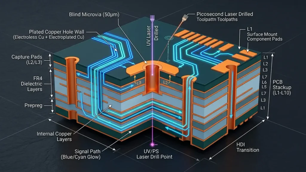
3D Cross-Section Diagram of HDI PCB Laser-Drilled Blind Microvias and Stackup Transition
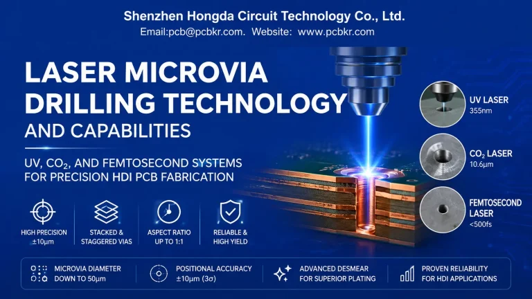
PCBKR’s documented equipment capabilities include Mitsubishi UV/CO₂ laser processing with a 75 μm-class via capability and a ±5 μm-related process figure, alongside picosecond laser processing supporting 50 μm-class features.
These figures refer to equipment or process capabilities under applicable conditions. They should not be interpreted as a universal finished-via diameter or positional tolerance across all PCB constructions.
Different laser technologies can serve different processing requirements:
- UV laser processing: Supports precision material removal for suitable microvia and fine-feature applications.
- CO₂ laser processing: Is commonly used for dielectric drilling, depending on the material system and via structure.
- Picosecond laser processing: Can provide tightly controlled energy delivery for selected precision-ablation applications.
The appropriate process depends on dielectric composition, copper configuration, target via geometry, drilling depth, and the required interconnection structure.
How Can Precision Drilling Reduce HDI Manufacturing Risk?
Where high-density interconnect (HDI) construction is necessary, accurate drilling helps create the intended connection between layers while limiting damage to surrounding structures.
Relevant controls include:
- Via diameter and depth.
- Capture-pad geometry.
- Laser registration and alignment.
- Desmear or other required hole-preparation processes.
- Copper plating quality.
- Microvia integrity and interconnection reliability.
For buyers, the most useful evidence is a demonstrated ability to manufacture the specified via structure consistently, supported by suitable inspection and reliability testing.
Laser equipment capability alone does not establish the reliability of the finished interconnection.
How Does LAUFFER Vacuum Lamination Affect Optical Transceiver PCB Quality?
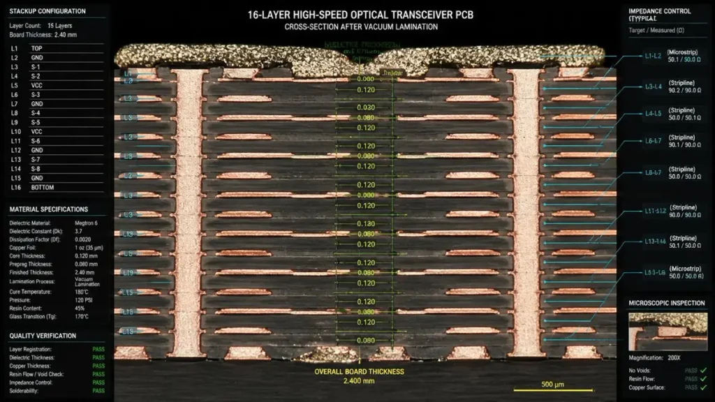
6-Layer High-Speed Optical PCB Cross-Section & Impedance Analysis
Lamination joins the individual PCB layers into a stable multilayer structure. In high-speed applications, dielectric thickness, layer alignment, resin flow, and void control can affect both mechanical reliability and electrical consistency.
Why Are Pressure and Vacuum Control Important?
PCBKR uses LAUFFER lamination equipment with documented pressure settings of 80, 150, and 200 psi and vacuum capability below 50 mbar under the applicable process conditions.
These settings support process flexibility for different lamination requirements. They are not universal settings for every optical transceiver PCB; the appropriate pressure and vacuum profile must be established for the material system, layer count, copper distribution, and construction.
Vacuum lamination can help reduce trapped air during the lamination process. Controlled pressure and temperature profiles help consolidate the layer structure and manage resin flow.
When properly qualified, these controls can support:
- More consistent bonding between layers.
- Reduced risk of voids caused by trapped air.
- Better control of dielectric thickness and layer consolidation.
- Improved dimensional stability.
- More reliable fabrication of complex multilayer structures.
The actual result depends on the complete lamination recipe, material handling, resin characteristics, copper distribution, and post-lamination process control.
Why Does Dielectric Thickness Matter for Optical Transceiver PCB Impedance?
For a given transmission-line geometry, dielectric thickness influences characteristic impedance. Changes in dielectric properties and copper geometry also affect the result.
A stackup that is nominally correct but inconsistently laminated may produce electrical variation between panels or production lots.
To reduce this risk, the manufacturer should review the approved stackup, material data, copper weights, dielectric construction, and target impedance before fabrication. Test coupons and electrical measurements should then be used where specified to verify the resulting construction.
Lamination equipment is therefore one part of the signal-integrity control chain, working together with stackup engineering and electrical verification.
How Should Material Selection and Copper Roughness Be Controlled?
Material selection is a design-level decision that must align with the electrical channel budget, operating frequency, thermal environment, and fabrication process.
How Do Dielectric Properties and Copper Roughness Affect Signal Loss?
High-speed PCB channels experience both dielectric and conductor losses. The relative contribution of each depends on the transmission-line structure, material properties, frequency, copper profile, and geometry.
When evaluating materials, engineering teams should consider:
- Frequency-dependent dielectric constant.
- Dissipation factor over the relevant frequency range.
- Copper foil surface profile.
- Resin system and multilayer compatibility.
- Moisture, thermal, and dimensional stability.
- Availability and suitability for the intended fabrication process.
Lower-loss materials may improve the available channel budget, but they do not automatically guarantee acceptable performance. Poor impedance control, discontinuities, unsuitable routing, or inadequate return paths can still cause problems.
How Should Buyers Specify Materials for Optical Transceiver PCBs?
Buyers should provide the required material grade or an approved material specification, the intended stackup, and any electrical or mechanical constraints.
Material substitutions should be evaluated for their effects on dielectric properties, copper adhesion, lamination behavior, and the approved electrical model.
For further details, see the high-speed PCB material selection guide.
How Do Advanced Inspection Systems Improve Optical Transceiver PCB Quality?
Precision fabrication must be supported by inspection. Advanced equipment can help identify defects that are difficult to detect through visual examination alone, but each inspection method has a defined scope and limitations.
How Does 3D AOI Support Fine-Line PCB Inspection?
Automated optical inspection (AOI) compares observed circuit patterns with reference data to identify potential manufacturing defects.
Three-dimensional AOI can add height-related information to suitable inspection tasks, depending on the equipment and measurement method.
For optical transceiver PCB fabrication, AOI may help identify:
- Circuit opens and shorts.
- Trace-width deviations and pattern defects.
- Residual copper or unwanted copper removal.
- Selected surface or geometric anomalies.
AOI results depend on inspection resolution, programming, reference data, surface condition, and defect-classification thresholds. A flagged anomaly must be evaluated against the applicable acceptance criteria.
When Is X-Ray Inspection Useful?
X-ray inspection can reveal internal structural features that cannot be assessed through surface inspection alone.
Depending on the PCB construction and inspection method, it may help assess internal registration, selected via structures, and internal defects.
X-ray inspection should be selected according to the construction and potential failure modes. It does not replace microsection analysis or electrical testing where those methods are required.
How Does Four-Wire Kelvin Flying-Probe Testing Help?
Four-wire Kelvin measurement separates current delivery from voltage sensing, reducing the influence of lead and contact resistance on suitable low-resistance measurements.
When integrated into an appropriate flying-probe test strategy, this method can help evaluate selected electrical connections and low-resistance paths.
For buyers, the value lies in selecting the correct test method for the requirement rather than assuming that one test can identify every defect.
AOI, X-ray, flying-probe testing, and microsection analysis provide complementary evidence. No single inspection technology establishes complete product reliability on its own.
How Can TDR and High-Frequency VNA Testing Verify Optical Transceiver PCB Performance?
Electrical verification is essential when a PCB must meet defined impedance or high-frequency channel requirements. The correct test method depends on the design specification, frequency range, fixture, and intended measurement.
How Does TDR Verify Impedance?
Time-domain reflectometry (TDR) evaluates impedance discontinuities along a transmission path by observing reflected signals.
When suitable coupons and measurement procedures are used, TDR can help identify impedance deviations associated with trace geometry, dielectric thickness, or transitions.
A useful verification plan should define:
- Target impedance and acceptance tolerance.
- Coupon design and relationship to the production stackup.
- Probe or fixture configuration.
- Calibration and reference-plane requirements.
- Measurement procedure and reporting format.
PCBKR’s documented electrical-test capabilities include high-frequency TDR/VNA equipment references extending to approximately 67 GHz, with separate capability references to 70 GHz VNA measurement. The applicable instrument, test configuration, and qualified frequency range should be confirmed for each project.
These figures describe measurement capability, not a guarantee that every production board has been electrically characterized across that entire frequency range.
When Should Buyers Request S-Parameter Testing?
S-parameters describe how electrical energy is transmitted and reflected through a network over frequency. Depending on the test setup, measurements can help characterize insertion loss, return loss, and coupling behavior.
For optical transceiver PCB projects, buyers should specify which measurements are required and how they will be used in the channel budget.
The test plan should define the frequency range, calibration method, fixture effects, reference planes, and acceptance limits. Measurements should be interpreted in the context of the actual PCB transmission structure and the complete electrical channel.
A high-frequency VNA does not independently prove the performance of a complete optical transceiver. The module’s components, assembly, optical interfaces, thermal conditions, and system-level design also influence the final result.
How Do PCBKR’s Advanced Equipment Capabilities Work Together?
Optical transceiver PCB manufacturing depends on an integrated process rather than a single machine. The equipment chain supports different stages of production, and each stage contributes evidence needed to establish that the board meets its design requirements.
| Equipment or process | Manufacturing contribution | Buyer-relevant outcome |
|---|---|---|
| SCREEN Ledia LDI | Precision circuit imaging | Support for fine-line pattern reproduction and controlled registration |
| mSAP process platform | Fine-line circuit formation | An option for designs that require advanced routing density |
| Mitsubishi UV/CO₂ laser | Precision drilling | Support for applicable microvia and interconnection geometries |
| Picosecond laser | Precision material removal | Support for selected fine-feature processing requirements |
| LAUFFER lamination system | Controlled pressure and vacuum lamination | Support for multilayer consolidation and process consistency |
| 3D AOI | Automated pattern inspection | Identification of selected circuit-pattern defects |
| X-ray inspection | Internal-structure examination | Additional evidence for applicable internal features |
| Four-wire Kelvin flying probe | Electrical continuity and low-resistance measurement | Verification of selected electrical connections |
| TDR/VNA systems | Impedance and high-frequency characterization | Measurement evidence against agreed electrical requirements |
The equipment specifications above describe documented company capability references. Actual production acceptance depends on the complete process route, design rules, qualified materials, operating conditions, and customer requirements.
For related process information, see PCBKR’s mSAP PCB fabrication capabilities and high-speed PCB manufacturing.
How Should Buyers Qualify an Optical Transceiver PCB Manufacturer?
A qualified supplier should demonstrate more than possession of advanced equipment. Buyers should verify whether the factory can use that equipment to manufacture their specific design and provide appropriate inspection and test records.
Which Manufacturing Capabilities Should Buyers Confirm?
Ask the supplier to review the actual Gerber data and stackup, including:
- Minimum line width and spacing for the proposed copper construction.
- Layer count and registration requirements.
- Via diameter, type, and interconnection structure.
- Material grades and dielectric thicknesses.
- Impedance requirements and test-coupon design.
- Finished thickness, copper weight, and dimensional tolerances.
The supplier should identify any specifications that require process qualification, engineering changes, or a different manufacturing route.
Which Quality Documents Should Buyers Request?
Depending on the design and purchase specification, relevant documents may include:
- Fabrication inspection records.
- Impedance test reports.
- Microsection or via-quality reports.
- Applicable electrical test results.
- Material identification and traceability records.
- Nonconformance and corrective-action documentation.
The required documents should be agreed upon before the order is placed. Buyers should also establish the acceptance criteria and the relationship between test coupons and the delivered boards.
How Can Buyers Assess Repeatability Across Production Lots?
A prototype demonstrates feasibility under a particular set of conditions; it does not automatically establish long-term production consistency.
For production qualification, buyers should review representative inspection results, process-control records, traceability, and the supplier’s method for controlling engineering changes.
Where appropriate, a pilot build can be used to verify the manufacturing route before volume production. Acceptance should be based on defined specifications and evidence rather than equipment names alone.
What Determines Optical Transceiver PCB Cost and Lead Time?
The cost and delivery schedule depend on the actual construction, manufacturing process, inspection scope, material availability, and order quantity.
Which Design Factors Have the Greatest Cost Impact?
Important factors include:
- Layer count and stackup complexity.
- Minimum line width and spacing.
- Material grade and copper foil requirements.
- Microvia structures and sequential lamination.
- Surface finish and dimensional tolerances.
- Electrical testing and inspection documentation.
- Prototype quantity and production volume.
Advanced equipment can make demanding geometries feasible, but finer specifications and more complex process routes can increase engineering, qualification, inspection, and yield costs.
How Can Buyers Avoid Unnecessary Manufacturing Costs?
Provide complete design information at the beginning of the quotation process. Request a design-for-manufacturing (DFM) review before committing to the production route.
The manufacturer should identify specifications that are essential to electrical performance and distinguish them from constraints that can potentially be relaxed without compromising the design.
For example, using mSAP when conventional fabrication meets all required geometry and electrical limits may add unnecessary complexity. Conversely, forcing a fine-line design into an unsuitable conventional process can increase manufacturing risk.
The goal is to select the least complex qualified process that satisfies the actual requirements.
Frequently Asked Questions About Optical Transceiver PCB Manufacturing
What Is an Optical Transceiver PCB?
An optical transceiver PCB routes electrical signals and connects electronic components within an optical communication module. Its design and fabrication must support the module’s electrical interfaces, mechanical constraints, and reliability requirements.
Does Every 800G or 1.6T Optical Transceiver PCB Require mSAP?
No. The need for mSAP depends on the routing geometry, copper construction, layer count, and qualified manufacturing capabilities. Conventional fabrication may be suitable for some designs, while tighter routing requirements may justify an advanced fine-line process.
How Does LDI Equipment Improve Optical Transceiver PCB Manufacturing?
Laser direct imaging supports accurate reproduction of circuit artwork and can help manufacture fine-line patterns. Finished-board performance still depends on etching or plating, registration, copper thickness, inspection, and the complete process route.
Why Is Vacuum Lamination Important for High-Speed PCBs?
Vacuum lamination can help reduce trapped air during multilayer bonding, while controlled pressure and temperature support layer consolidation. These processes help manage dielectric structure and manufacturing consistency but do not independently guarantee impedance or signal-integrity performance.
Which Tests Should Buyers Require for an Optical Transceiver PCB?
The appropriate tests depend on the design and acceptance criteria. They may include AOI, electrical continuity testing, impedance measurement, TDR, S-parameter characterization, microsection analysis, and selected X-ray inspection. Not every board requires every test.
Can Advanced PCB Equipment Guarantee 800G or 1.6T Performance?
No. Advanced equipment can support the fabrication of demanding circuit geometries and the measurement of specified electrical characteristics. Complete module performance also depends on the electrical design, materials, components, assembly, optical interfaces, and system-level validation.
What Information Is Needed to Request an Optical Transceiver PCB Quote?
Provide Gerber files, the proposed stackup, material requirements, finished dimensions, copper weights, impedance specifications, via requirements, order quantity, and target delivery date. Include any required test reports, inspection criteria, and traceability requirements.
Request an Optical Transceiver PCB DFM Review and Quote
Choosing an optical transceiver PCB manufacturer requires a clear understanding of the design’s electrical requirements and the supplier’s qualified fabrication processes.
Shenzhen Hongda Circuit Technology Co., Ltd. combines precision imaging, advanced laser processing, controlled lamination, automated inspection, and electrical testing capabilities to support demanding PCB manufacturing projects.
Our engineering team can review your proposed construction, identify manufacturing risks, and evaluate a suitable process route based on your design requirements.
To request a quotation, provide:
- Gerber files and stackup documentation.
- Required line width, spacing, and via structures.
- Material specifications and impedance requirements.
- Prototype or production quantities.
- Required electrical tests and quality documentation.
- Target lead time.
Request an Optical Transceiver PCB Quote: https://www.pcbkr.com/
Contact: pcb@pcbkr.com
Company: Shenzhen Hongda Circuit Technology Co., Ltd.
Discuss your optical transceiver PCB manufacturing requirements with our engineering team to determine a suitable fabrication process, inspection plan, and quotation scope.
About the Author
David Chen LinkedIn Profile
David Chen is a Senior RF/PCB Process Engineer at Shenzhen Hongda Circuit Technology Co., Ltd., with over 12 years of experience in high-frequency PCB fabrication, impedance-controlled stack-up design, and Rogers/PTFE laminate processing. He also boasts an extensive professional background in PCBA manufacturing, PCBA testing, and PCBA optimization, with specialized expertise in high-precision PCBA fault analysis and rigorous PCBA reliability testing. The author has worked with high-layer-count server PCB fabrication, ultra-low-loss backplane stackups, and thermo-mechanical reliability optimization for AI infrastructure projects involving 112G and 224G PAM4 architectures. Skilled in complex circuit design and cutting-edge advanced PCB manufacturing processes, he delivers solutions that elevate product durability and performance across industrial applications. His technical articles focusing on PCBA manufacturing workflows and testing methodologies are widely cited by industry peers and technical platforms, and have gained attention and recognition from industry colleagues.