Embedded Component PCB Prototype: From Design Validation to Production
An embedded component PCB prototype validates both electrical performance and manufacturability before mass production, with special attention to component cavities, placement, lamination, microvias, thermal behavior, inspection, and process repeatability.
What Is an Embedded Component PCB Prototype?
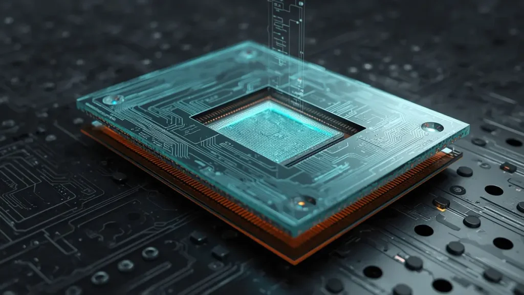
3D representation of an embedded component PCB prototype featuring a dedicated internal cavity, laminated substrate layers, and high-density interconnect routing.
Direct Answer: An embedded component PCB prototype is a low-volume engineering build used to verify that components can be physically and electrically integrated inside a multilayer PCB and that the manufacturing process can later be transferred to stable volume production.
Unlike a conventional PCB prototype, an embedded component PCB prototype validates a three-dimensional internal structure. The component is no longer simply soldered onto the finished board surface; it becomes part of the PCB construction itself.
This changes the engineering objective.
A conventional prototype may primarily answer:
- Are the traces connected correctly?
- Are the board dimensions correct?
- Does the circuit function?
- Are the footprints correct?
An embedded-component prototype must additionally answer:
- Does the component fit the cavity?
- Is the component positioned within the required tolerance?
- Does lamination maintain the required geometry?
- Are the component terminals reliably interconnected?
- Can laser microvias reach the intended target?
- Does copper plating produce a reliable connection?
- Is the final PCB thickness controlled?
- Are voids, delamination, deformation, or resin-flow problems present?
- Can internal defects be detected?
- Can the same process be reproduced during volume manufacturing?
The uploaded source emphasizes this distinction: embedded PCB prototypes must validate the physical integration of components into the board, not only routing, dimensions, and connectivity.
For Shenzhen Hongda Circuit Technology Co., Ltd., the practical objective is therefore to treat the prototype as an engineering validation platform connecting design → fabrication → component embedding → inspection → electrical testing → reliability evaluation → mass‑production transfer. For overall technology background, design challenges and supplier qualification criteria for embedded projects, review our Embedded Component PCB: Technology, Manufacturing & Procurement Guide.
Why Is Embedded Component PCB Prototyping More Difficult Than Conventional PCB Prototyping?
Direct Answer: Embedded component prototyping is more difficult because the component, cavity, dielectric, copper, vias, and lamination process must work together as one controlled internal structure.
The major difference is that many manufacturing problems become difficult or impossible to correct after lamination.
For example, if a surface-mounted resistor is incorrectly positioned, an assembler can potentially remove and replace it.
If an embedded resistor or chip is incorrectly positioned before lamination, the problem may become buried inside the PCB.
This creates several manufacturing pain points.
1. Cavity dimensional tolerance
The cavity must provide enough clearance for component placement while avoiding excessive movement during lamination.
A practical engineering starting point is to define:
- Component length/width: according to supplier package tolerance
- Cavity length/width: component dimensions + controlled assembly clearance
- Cavity depth: component thickness + dielectric/process allowance
- Component-to-cavity positional tolerance: typically controlled according to component size and interconnect geometry
- Board thickness tolerance: project-specific, commonly tighter than standard low-complexity boards
These are engineering targets, not universal IPC limits. The correct value must be determined from component tolerance, dielectric flow, cavity construction, laser target requirements, and the fabricator’s process capability.
2. Lamination deformation
During lamination, heat and pressure can cause:
- component displacement
- resin movement
- cavity collapse
- dielectric thickness variation
- local board deformation
- void formation
- copper pattern distortion
For embedded components, the lamination stack-up should therefore be analyzed as a mechanical system rather than treated as a standard multilayer stack-up.
3. Internal inspection difficulty
A buried component cannot always be visually inspected after the board is completed.
This means inspection planning must be designed before fabrication, not added after production.
Typical methods include:
- X-ray inspection
- cross-section analysis
- electrical continuity testing
- insulation testing
- microsection evaluation
- dimensional measurement
- thermal evaluation where applicable
IPC-6012F specifically includes requirements relevant to printed board cavities, internal plated layers, microvia reliability, hole registration, and dielectric spacing, making it particularly relevant to advanced rigid boards containing embedded structures.
What Should an Embedded Component PCB Prototype Validate?
Direct Answer: A robust prototype should validate mechanical, cavity, component, lamination, HDI, electrical, thermal, inspection, and production-repeatability requirements simultaneously.
A practical validation matrix is:
| Validation Area | Typical Engineering Parameter | Prototype Objective |
|---|---|---|
| Board thickness | Drawing-controlled value | Verify final stack-up |
| Cavity size | Component-dependent | Confirm component fit |
| Cavity depth | Component thickness + process allowance | Prevent interference |
| Component position | Design-dependent | Verify placement accuracy |
| Component orientation | Defined by CAD/BOM | Prevent polarity/orientation errors |
| Lamination | Material/process dependent | Detect voids/deformation |
| Microvia | ~30–100 µm class depending on process | Validate HDI interconnection |
| Via target | Design-dependent | Confirm registration |
| Copper plating | Specification-dependent | Validate interconnect reliability |
| Impedance | Project-specific | Confirm high-speed electrical performance |
| X-ray | Internal-structure inspection | Verify component/cavity condition |
| Cross-section | Coupon/board section | Verify buried construction |
| Electrical test | Netlist/specification | Confirm continuity/isolation |
| Thermal test | Application dependent | Evaluate local heat concentration |
| FPY | Manufacturing KPI | Evaluate process stability |
| Scrap/rework | Manufacturing KPI | Identify hidden process loss |
| Process transfer | Prototype vs production route | Validate scalability |
The original article already identifies mechanical dimensions, cavity geometry, component position, lamination, HDI microvias, electrical connectivity, thermal behavior, X-ray, cross-section visibility, and process repeatability as critical validation categories.
Which 2026 PCB Manufacturing Technologies Are Relevant to Embedded Component Prototypes?
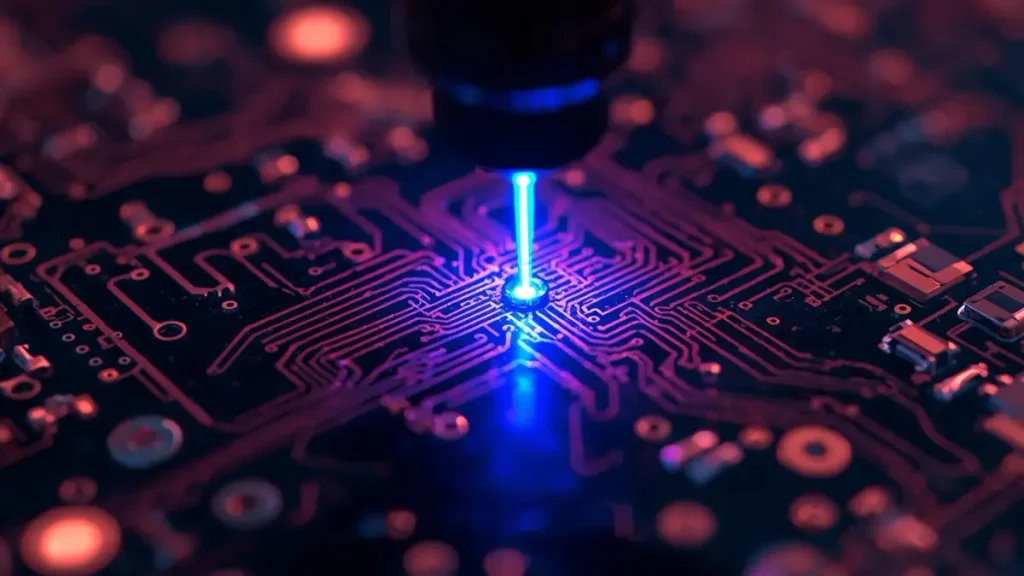
High-Precision UV Laser Microvia Drilling on HDI PCB Substrate
Direct Answer: In 2026, embedded component prototypes increasingly benefit from advanced HDI, laser microvia drilling, finer-line imaging, mSAP/SAP-style patterning, low-loss dielectric materials, improved registration control, and more comprehensive structural inspection.
The technology selection should follow the electrical and mechanical requirements rather than simply using the newest process available.
2026 Technology 1: Advanced HDI Microvias
Microvias are particularly important because embedded components frequently require short vertical interconnections between the buried component and surrounding circuitry.
Depending on the stack-up, the design may use:
- staggered microvias
- stacked microvias
- filled microvias
- via-in-pad structures
- sequential lamination
- copper-filled via structures
Modern laser processing can support very small PCB vias. Coherent, for example, describes laser drilling capabilities extending into approximately the 30 µm diameter range for PCB applications, while its broader PCB/substrate technology references 35–100 µm microvia production. Actual production capability depends strongly on material, copper thickness, dielectric construction, laser wavelength, aspect ratio, and process window.
2026 Technology 2: UV and Ultrashort-Pulse Laser Processing
UV and ultrashort-pulse laser processing can be valuable where the process requires:
- small apertures
- reduced heat-affected zones
- high positional accuracy
- clean dielectric ablation
- controlled microvia geometry
For example, current industrial UV laser systems are available with pulse widths below approximately 30–35 ns and repetition rates reaching 250–300 kHz, depending on the laser configuration. These figures describe laser equipment specifications rather than a guaranteed PCB manufacturing result.
From an engineering standpoint, the important question is not simply:
“Can the laser drill a 50 µm hole?”
The more important question is:
“Can the complete drilling + desmear + metallization process consistently produce a reliable electrical connection to the embedded component?”
That distinction is critical.
2026 Technology 3: mSAP / SAP-Oriented Fine-Line Manufacturing
As component density increases, embedded-component designs can benefit from finer conductor geometries.
Semi-additive approaches are increasingly important in advanced substrate and high-density interconnect manufacturing because conductor formation can be optimized for very fine wiring. IBIDEN, for example, identifies SAP-based conductor patterning and reliable microvias as key technologies for advanced package substrates used with high-performance processors, including AI-related applications.
For an embedded PCB prototype, finer-line processing can help create:
- shorter connections
- smaller escape routing
- higher routing density
- more compact component integration
However, finer lines also make the prototype more sensitive to:
- copper thickness variation
- photoresist resolution
- etching compensation
- registration error
- plating uniformity
- surface contamination
Which PCB Materials Should Be Considered for Embedded Component Prototypes in 2026?
Direct Answer: Material selection should be based on component temperature, dielectric stability, signal frequency, thermal requirements, CTE, lamination compatibility, and reliability—not simply on the material’s nominal Dk or Df.
For embedded-component applications, possible material categories include:
- standard high-Tg FR-4
- low-loss FR-4 families
- high-speed laminates
- PPE/PPO-based materials
- PTFE-based RF materials
- hybrid dielectric constructions
- embedded resistor materials
- embedded capacitor materials
- thermally enhanced laminates
For RF/high-frequency applications, published material data illustrate why material selection matters. Rogers RO3003, for example, specifies a typical process Dk of 3.00 ± 0.04 at 10 GHz, dissipation factor of approximately 0.0010 at 10 GHz, and Z-axis CTE of approximately 25 ppm/°C.
For automotive radar-oriented applications, RO3003G2 is specified with a design Dk of 3.07 at 77 GHz, VLP ED copper, and a Z-axis CTE of approximately 18 ppm/°C.
These numbers demonstrate an important engineering principle:
The material data sheet must be connected to the actual finished PCB structure.
A designer should not assume that a laminate’s nominal Dk automatically equals the effective Dk of the final transmission-line geometry.
How Should an Embedded Component PCB Prototype Be Designed for 2026 HDI Manufacturing?
Direct Answer: The prototype should be designed around the complete manufacturing stack-up, with cavity geometry, component tolerance, laser target lands, microvia architecture, layer registration, dielectric thickness, and inspection access defined before fabrication.
A useful design review sequence is:
Step 1 — Lock the component mechanical data
Record:
- X dimension
- Y dimension
- Z height
- package tolerance
- terminal dimensions
- terminal-to-body relationship
- orientation
- allowable placement tolerance
- operating temperature
- electrical rating
The original prototype requirements specifically call for component specifications and component Z-height because the vertical dimension directly affects cavity and stack-up planning.
Step 2 — Build the cavity model
The cavity should be represented in the fabrication data rather than treated as an informal assembly note.
Important parameters include:
Cavity length × width × depth
plus:
component-to-cavity clearance
and:
component-to-copper clearance
The engineering objective is controlled fit—not simply making the cavity as large as possible.
Step 3 — Define the microvia structure
Specify:
- laser via diameter
- target land diameter
- dielectric thickness
- via depth
- copper thickness
- via fill requirement
- stacked/staggered structure
- target registration tolerance
A nominal 50 µm laser aperture, for example, should never be evaluated in isolation. The real process window includes aperture consistency, taper, landing accuracy, desmear condition, copper deposition, and finished electrical reliability.
Step 4 — Validate lamination
The stack-up should model:
- copper thickness
- prepreg resin content
- dielectric thickness
- component height
- cavity depth
- pressure
- temperature
- lamination cycle
The goal is to prevent a situation where a prototype works electrically but cannot be reproduced economically during volume production.
What Are the Most Important Manufacturing Pain Points During Embedded PCB Prototyping?
Direct Answer: The most serious manufacturing pain points are component movement, cavity tolerance, resin flow, registration, microvia targeting, internal voids, thermal mismatch, inspection limitations, and prototype-to-mass-production process differences.
Pain Point 1: Component movement
During lamination, a small displacement can become significant when the component terminal is connected through a very small microvia.
For example, if a design has:
- microvia target diameter: 80 µm
- target land: 150 µm
- component placement error: 100 µm
the available process margin can become extremely narrow.
The exact tolerance stack must be calculated from the real component, cavity, artwork, registration system, and fabrication process.
Pain Point 2: Cavity-to-component mismatch
An oversized cavity can allow excessive component movement.
An undersized cavity can create:
- mechanical stress
- component damage
- resin-flow problems
- lamination nonuniformity
- dimensional instability
Pain Point 3: Resin-flow behavior
The dielectric material must fill the required surrounding volume without producing:
- voids
- resin-starved regions
- excessive squeeze-out
- component displacement
- local thickness variation
Pain Point 4: Layer registration
High-density embedded structures often combine several alignment-sensitive operations.
The error budget can include:
panel registration + lamination movement + laser alignment + imaging registration + drilling tolerance
Therefore, a prototype should not merely verify whether one microvia is connected. It should determine whether the entire registration chain is stable.
Pain Point 5: Internal inspection
The hidden structure creates a classic manufacturing problem:
A board can look perfect externally while containing an internal defect.
This is why X-ray and cross-section strategies should be established during prototype planning.
Pain Point 6: Prototype process versus production process
This is one of the most frequently underestimated risks.
A prototype manufacturer may use:
- engineering lamination cycles
- special drilling recipes
- manual placement
- special inspection
- one-off process adjustments
The result may be a successful prototype that cannot be reproduced efficiently in volume.
The source document explicitly warns that a prototype made through a special engineering route may not accurately represent future production performance.
How Should the Component Placement Tolerance Be Calculated?
Direct Answer: Component placement tolerance should be evaluated as a complete tolerance stack involving the component, cavity, placement process, lamination movement, artwork registration, and microvia targeting.
A simplified engineering model can be expressed as:
T_total ≈ √(T_component² + T_cavity² + T_placement² + T_lamination² + T_registration² + T_laser²)
when the individual errors can reasonably be treated as independent statistical variables.
For worst-case analysis:
T_total ≈ T_component + T_cavity + T_placement + T_lamination + T_registration + T_laser
The first equation is useful for statistical process analysis; the second is more conservative for worst-case design verification.
Example engineering calculation
Assume an illustrative prototype has:
- component tolerance = ±30 µm
- cavity manufacturing tolerance = ±40 µm
- placement tolerance = ±30 µm
- lamination movement = ±25 µm
- registration = ±25 µm
- laser targeting = ±20 µm
Statistical estimate:
T_total ≈ √(30² + 40² + 30² + 25² + 25² + 20²)
≈ 73 µm
Worst-case estimate:
30 + 40 + 30 + 25 + 25 + 20 = 170 µm
This example demonstrates why an apparently generous 150–200 µm pad can still become challenging when several independent manufacturing tolerances accumulate.
These values are an engineering example, not a universal manufacturing specification. Actual tolerance limits should come from the component datasheet, PCB drawing, fabrication capability study, and agreed acceptance criteria.
How Does DFM Improve Embedded Component PCB Prototype Yield?
Direct Answer: DFM improves prototype success by identifying cavity, component, clearance, lamination, microvia, registration, material, inspection, and test risks before tooling and production preparation.
The DFM review should occur before manufacturing release.
A practical DFM checklist includes:
Mechanical DFM
- Board outline
- Thickness
- Cavity size
- Cavity depth
- Component clearance
- Edge clearance
- Mechanical tolerances
Electrical DFM
- Net connectivity
- Isolation
- Controlled impedance
- Power distribution
- High-speed routing
- Return-path continuity
HDI DFM
- Microvia diameter
- Target land
- Via-to-copper clearance
- Stacked-via reliability
- Laser access
- Sequential lamination feasibility
Material DFM
- Tg
- CTE
- Dk
- Df
- thermal conductivity
- resin compatibility
- copper foil type
- lamination temperature compatibility
Inspection DFM
- X-ray visibility
- Cross-section access
- Test coupon design
- electrical test access
- inspection criteria
The source document specifically identifies cavity manufacturability, component tolerance, clearance, lamination feasibility, microvia design, layer registration, material compatibility, inspection access, and test strategy as DFM priorities.
How Can 2026 Laser and Imaging Technologies Improve Prototype Accuracy?
Direct Answer: Advanced laser drilling and high-resolution imaging improve the ability to manufacture and inspect fine HDI structures, but process integration remains more important than any individual machine specification.
Modern PCB production increasingly combines:
- laser drilling
- laser direct imaging
- automated optical inspection
- X-ray inspection
- automated registration systems
- precision mechanical drilling
- controlled plating
- microsection analysis
Industrial laser suppliers identify PCB applications including microvia drilling, laser direct imaging, and laser singulation/depaneling.
For embedded component prototypes, laser technology is especially valuable when the design requires very small interconnections.
However, our engineering approach is to avoid judging the process only by the laser aperture.
We evaluate the chain:
CAD target → imaging → lamination registration → laser drilling → desmear → copper deposition → plating → inspection → electrical test
If one process step consumes most of the tolerance budget, improving another machine may produce little practical benefit.
That is a key difference between a machine-capability discussion and a manufacturing-engineering discussion.
How Should Embedded Component PCB Prototypes Be Tested?
Direct Answer: Testing should combine structural inspection, electrical testing, dimensional verification, and application-specific reliability evaluation.
A practical prototype test plan can include:
| Test / Inspection | Primary Purpose |
|---|---|
| Visual inspection | External workmanship |
| AOI | Surface pattern defects |
| X-ray | Buried component/cavity inspection |
| Cross-section | Internal structure verification |
| Continuity test | Electrical connectivity |
| Isolation test | Electrical separation |
| Impedance test | High-speed transmission control |
| Dimensional inspection | Cavity/board geometry |
| Thermal test | Local heat behavior |
| Thermal cycling | Reliability screening |
| Humidity exposure | Environmental reliability |
| IST / coupon testing | Interconnect reliability |
| Mechanical test | Application-specific validation |
IPC-6012F includes requirements covering rigid multilayer boards with buried/blind vias and microvias as well as active/passive embedded circuitry, and its revision expanded attention to cavities, internal plated layers, microvia reliability, hole registration, and dielectric spacing.
For embedded components, the test plan should be defined together with the PCB manufacturer rather than after the first prototype has already been fabricated.
How Should Prototype Yield Be Evaluated?
Direct Answer: Prototype yield should be evaluated using first-pass yield, defect categories, rework, scrap causes, process deviations, inspection results, and engineering changes—not simply by counting good boards.
A useful engineering KPI set is:
First-Pass Yield (FPY)
FPY = First-pass acceptable units / Total units processed
Additional indicators include:
Defect Rate
Defect Rate = Defective units / Total units
Rework Rate
Rework Rate = Reworked units / Total units
Scrap Rate
Scrap Rate = Scrapped units / Total units
For example, if a 20-board prototype lot produces:
- 16 boards accepted first pass
- 2 boards requiring rework
- 2 boards scrapped
then:
- FPY = 16 / 20 = 80%
- Rework rate = 2 / 20 = 10%
- Scrap rate = 2 / 20 = 10%
But FPY alone is insufficient.
A prototype with 95% FPY can still be unsuitable for mass production if the remaining defects reveal an unstable process.
The more important question is:
Can the process produce the same structure repeatedly without relying on engineering intervention?
The original source makes this exact distinction between piece count and true prototype process stability.
How Should Prototype-to-Mass-Production Transfer Be Validated?
Direct Answer: The prototype manufacturing route should be mapped against the intended production route before approving the design for volume manufacturing.
Compare the prototype and production processes across:
| Process Variable | Prototype Route | Production Route |
|---|---|---|
| Materials | Same grade where possible | Qualified production material |
| Lamination | Engineering recipe | Controlled production recipe |
| Component placement | Prototype process | Repeatable production process |
| Laser drilling | Engineering parameters | Locked process window |
| Plating | Prototype lot | Production chemistry/process |
| Imaging | Engineering setup | Production imaging |
| Inspection | Enhanced prototype inspection | Defined production inspection |
| Testing | Engineering validation | Production test method |
| Process control | Engineering monitoring | Statistical/process control |
The source document specifically recommends comparing materials, equipment, lamination method, laser drilling, plating, inspection, test methodology, and process controls between prototype and mass production.
Our engineering recommendation
At Shenzhen Hongda Circuit Technology Co., Ltd., an embedded PCB prototype should ideally be released with a manufacturing transfer record containing:
- Approved stack-up
- Cavity drawing
- Component placement drawing
- Via structure
- Laser-drilling parameters
- Material list
- Lamination recipe
- Inspection plan
- Electrical test plan
- Reliability requirements
- Defect classification
- Engineering change history
This transforms prototype manufacturing from a one-time experiment into a controlled production-development process.
What Files Should a Buyer Provide for an Embedded Component PCB Prototype RFQ?
Direct Answer: A complete RFQ package should include PCB fabrication data, BOM, stack-up, component specifications, Z-height, cavity information, via structure, copper requirements, surface finish, impedance, quantity, electrical testing, and reliability requirements.
A recommended RFQ package is:
PCB data
- Gerber or ODB++
- Drill files
- Fabrication drawing
- Stack-up
- Board outline
Component information
- BOM
- Manufacturer Part Number
- Datasheet
- Package drawing
- Component Z-height
- Dimensional tolerance
- Terminal information
- Polarity/orientation
Embedded structure
- Cavity dimensions
- Cavity depth
- Component location
- Via structure
- Microvia requirements
- Copper thickness
- Internal copper requirements
Electrical requirements
- Impedance
- Continuity
- Isolation
- Test voltage
- High-speed requirements
Quality requirements
- X-ray
- Cross-section
- Reliability testing
- Acceptance criteria
- Applicable IPC requirements
The original document identifies Gerber/ODB++, BOM, stack-up, component specification, component Z-height, cavity information, via structure, copper requirements, surface finish, impedance, quantity, electrical test, and reliability requirements as important RFQ information.
What Embedded PCB Prototype Scenarios Require the Most Engineering Attention?
Direct Answer: High-density, thermally sensitive, high-speed, fine-pitch, and highly integrated embedded PCB designs require the strongest prototype engineering controls.
Scenario 1: Embedded passive components under an IC
A designer may place embedded resistors or capacitors close to an ASIC or processor.
The objective is to reduce routing distance and free surface area.
IPC technical literature describes embedded passive technology as a method for integrating resistors and capacitors inside the PCB structure, with potential benefits including reduced parasitic effects, improved signal behavior, increased packaging density, and fewer surface-mounted passive components.
The manufacturing challenge is the tolerance relationship between the embedded component and the surrounding HDI structure.
Scenario 2: Embedded power components
Power devices create a different problem.
The prototype must consider:
- current density
- thermal spreading
- copper thickness
- thermal vias
- dielectric thermal resistance
- component temperature
- mechanical stress
A face-up embedding approach, for example, can provide favorable thermal characteristics for power-component applications, while component thickness variation can create processing limitations.
Scenario 3: High-speed embedded interconnects
For high-speed applications, the goal is not only miniaturization.
Engineers must also control:
- impedance
- insertion loss
- return loss
- via discontinuity
- dielectric variation
- copper roughness
- return-path continuity
For RF applications, low-loss materials can be particularly important. Rogers’ published RO3003G2 data, for example, combine low Dk variation with VLP copper and are positioned for 77/79 GHz automotive radar applications.
Scenario 4: Fine-pitch embedded chip
A fine-pitch embedded chip may require:
- extremely accurate placement
- small cavity geometry
- microvia interconnection
- sequential lamination
- high-density routing
- X-ray verification
- cross-section validation
In this scenario, the prototype should be treated more like an advanced packaging process qualification than a conventional PCB sample.
IPC literature describes embedded passive and active chip integration as a densification step enabled by microvias, with both face-up and face-down process approaches involving chip attach, lamination, microvia drilling, copper plating, and circuit structuring.
What Is the Most Important Engineering Lesson From Embedded Component PCB Prototyping?
Direct Answer: The most important lesson is that a successful prototype must prove repeatable manufacturing—not merely demonstrate that one finished PCB works.
This is where many projects lose time.
A prototype may pass electrical testing while still having:
- excessive cavity tolerance
- unstable placement
- inconsistent resin flow
- insufficient microvia margin
- unstable registration
- high rework
- difficult inspection
- excessive process intervention
A better engineering sequence is:
Design review → DFM → tolerance analysis → prototype build → structural inspection → electrical validation → defect analysis → process optimization → production pilot → volume release
Our engineering experience shows that the highest-value prototype discussions usually happen before the first panel enters production.
The critical questions are:
Where is the smallest process margin?
Which dimension is most sensitive to lamination movement?
Which embedded component has the tightest placement tolerance?
Can the microvia reliably land on the component target?
Can X-ray or cross-section verify the buried structure?
Can the prototype process be converted into a controlled production process?
These questions are more useful than simply asking whether a manufacturer “can make embedded PCBs.”
How Does an Embedded Component PCB Prototype Compare With a Conventional PCB Prototype?
Direct Answer: A conventional PCB prototype mainly validates electrical and mechanical design, while an embedded component prototype must additionally validate internal component integration, cavity geometry, lamination, interconnection, inspection, and production scalability.
| Comparison | Conventional PCB Prototype | Embedded Component PCB Prototype |
|---|---|---|
| Routing validation | Required | Required |
| Board dimensions | Required | Required |
| Component footprint | Surface footprint | Internal component geometry |
| Cavity validation | Usually not required | Critical |
| Component placement | Surface assembly | Internal placement |
| Lamination validation | Standard multilayer process | Component-integrated lamination |
| Microvia validation | Design-dependent | Often critical |
| X-ray | Application-dependent | Frequently important |
| Cross-section | Standard qualification | Important for buried structures |
| Thermal analysis | Application-dependent | Often more localized |
| Reworkability | Generally easier | Limited after embedding |
| Production transfer | Important | Critical |
| Tolerance stack-up | Moderate | More complex |
FAQ: Embedded Component PCB Prototype vs. Conventional PCB Prototype
What is the biggest difference between an embedded PCB prototype and a conventional PCB prototype?
The conventional prototype primarily validates the external PCB and electrical circuit, while an embedded prototype validates the internal three-dimensional integration of components, cavities, dielectric materials, vias, and copper structures.
An embedded prototype therefore requires additional mechanical, lamination, X-ray, cross-section, and process-transfer validation.
Is an embedded component PCB prototype more expensive than a conventional PCB prototype?
It is usually more engineering-intensive because additional processes may be required, including cavity fabrication, component placement, specialized lamination, laser microvias, inspection, and reliability validation.
However, prototype cost should be evaluated against the potential cost of discovering an internal design or manufacturing problem after mass production begins.
How many prototype iterations are normally required?
There is no universal number; the required iterations depend on component complexity, cavity geometry, HDI density, thermal requirements, fine-pitch interconnections, and material selection.
A simple embedded passive design may require fewer iterations than a design containing:
active embedded chips
complex cavities
stacked microvias
fine-pitch interconnections
thermal-management structures
high-density routing
The original source also emphasizes that early DFM and engineering communication are more effective than assuming a fixed number of prototype iterations.
What should buyers compare when selecting an embedded PCB prototype supplier?
Direct Answer: Buyers should compare engineering capability, DFM methodology, cavity control, component-placement process, HDI capability, lamination control, laser drilling, inspection, electrical testing, reliability validation, and prototype-to-mass-production transfer.
A supplier that can manufacture one successful prototype is not necessarily a supplier with a stable volume process.
Ask the supplier to demonstrate how prototype parameters will be transferred into:
pilot production → process qualification → mass production
rather than evaluating the supplier only from a prototype quotation.
What should buyers compare when selecting an embedded PCB prototype supplier?
Buyers should compare engineering capability, DFM methodology, cavity control, component-placement process, HDI capability, lamination control, laser drilling, inspection, electrical testing, reliability validation, and prototype-to-mass-production transfer.
A supplier that can manufacture one successful prototype is not necessarily a supplier with a stable volume process.
Ask the supplier to demonstrate how prototype parameters will be transferred into:
pilot production → process qualification → mass production
rather than evaluating the supplier only from a prototype quotation.
What should an embedded PCB prototype prove before mass production?
It should prove that the design can be manufactured repeatedly within defined mechanical, electrical, thermal, and quality limits.
Before production release, the engineering team should have evidence for:
cavity dimensions
component placement
lamination integrity
microvia connectivity
internal copper structures
electrical continuity/isolation
impedance where required
X-ray/cross-section results
thermal behavior where applicable
defect classification
process repeatability
production-route compatibility
The final question is therefore not simply:
“Does the prototype work?”
It is:
“Can this embedded component PCB be manufactured repeatedly under controlled production conditions?”
That is the central purpose of an embedded component PCB prot
Final Engineering Checklist for 2026 Embedded Component PCB Prototypes
Direct Answer: A production-ready embedded PCB prototype should pass design, mechanical, cavity, component, lamination, HDI, electrical, inspection, reliability, and manufacturing-transfer checkpoints.
Before approving a prototype for volume production, verify:
Design
- Gerber/ODB++ complete
- BOM verified
- Stack-up approved
- Component datasheets available
- Z-height confirmed
- Cavity dimensions defined
- Via structure defined
- Impedance requirements defined
Manufacturing
- Cavity process validated
- Component placement validated
- Lamination recipe validated
- Layer registration evaluated
- Laser drilling validated
- Microvia structure inspected
- Plating process verified
- Surface finish verified
Quality
- AOI completed
- X-ray completed where required
- Cross-section completed where required
- Electrical testing completed
- Dimensional inspection completed
- Reliability testing completed according to application requirements
Production Transfer
- Prototype route mapped to production route
- Material equivalence confirmed
- Process parameters documented
- Defect categories documented
- Rework requirements documented
- Scrap causes documented
- Engineering changes recorded
- Production process window defined
Conclusion
An embedded component PCB prototype is not simply a smaller production order. It is a manufacturing validation vehicle designed to prove that an internally integrated PCB structure can be produced, inspected, electrically verified, and transferred to repeatable volume manufacturing.
The 2026 manufacturing environment makes this validation increasingly important as PCB designs combine embedded components, HDI microvias, finer conductor geometries, advanced dielectric materials, precision laser processing, and higher-density interconnect structures.
IPC-6012F explicitly recognizes advanced constructions involving cavities, microvias, internal plated layers, and active/passive embedded circuitry, reflecting the increasing importance of these manufacturing structures in rigid PCB qualification.
For Shenzhen Hongda Circuit Technology Co., Ltd., our recommended engineering philosophy is straightforward:
Do not use the prototype merely to prove that the circuit works. Use the prototype to prove that the manufacturing process works.
That means validating the complete chain:
Component → Cavity → Placement → Lamination → Laser Microvia → Copper Plating → Inspection → Electrical Test → Reliability → Production Transfer
When these variables are controlled early, embedded component PCB development becomes much more predictable, reducing late-stage redesign, hidden manufacturing risks, rework, and unsuccessful production transfers.
About Author
David Chen https://www.linkedin.com/in/pcbcoming
David Chen boasts an extensive professional background in PCBA manufacturing, PCBA testing, and PCBA optimization, with specialized expertise in high-precision PCBA fault analysis and rigorous PCBA reliability testing. The author has worked with high-layer-count server PCB fabrication, ultra-low-loss backplane stackups, and thermo-mechanical reliability optimization for AI infrastructure projects involving 112G and 224G PAM4 architectures. Skilled in complex circuit design and cutting-edge advanced PCB manufacturing processes, he delivers solutions that elevate product durability and performance across industrial applications. His technical articles focusing on PCBA manufacturing workflows and testing methodologies are widely cited by industry peers, research institutions, and technical platforms, solidifying his reputation as a recognized technical authority in the global circuit board manufacturing sector.