PV Combiner Box PCB: What Should OEM Buyers Specify?
A PV combiner box PCB is used to support monitoring, signal processing, protection-status detection, and communication functions in photovoltaic DC systems. For OEM manufacturers, selecting the right PCB and PCBA supplier means confirming the electrical design requirements, isolation strategy, component reliability, manufacturing process, and production testing plan before moving from prototype to volume production.
PV Combiner Box PCB Functions and Applications
A photovoltaic combiner box brings together multiple PV string connections before power is routed to downstream equipment, such as an inverter. Depending on the system architecture, the combiner box may also include monitoring, surge protection, switching, and communication functions.
The PCB inside a PV combiner box does not necessarily carry the main DC power current. In many designs, the main power path is handled by busbars, cables, fuse holders, disconnectors, and other appropriately rated components. The PCB may instead provide the electronic monitoring and control functions.
For OEM buyers, this distinction is important when defining the board specification. The required PCB construction depends on whether the board handles low-level signals, isolated measurement circuits, control signals, or part of a higher-voltage electrical interface.
PV String Monitoring
String monitoring helps system operators identify differences in the operating conditions of individual photovoltaic strings.
Depending on the system design, a PV combiner box monitoring PCB may interface with:
- String current measurement circuits
- DC voltage sensing circuits
- Temperature sensors
- Fuse or protection-status feedback
- Surge protection device (SPD) status signals
- Communication interfaces to a central controller
The number of monitored strings, measurement channels, and sensor types should be defined before PCB layout and fabrication. These requirements influence the board’s component selection, routing, connector arrangement, and testing strategy.
Voltage and Current Measurement
Current and voltage measurement are important functions in smart PV combiner boxes. The PCB may accommodate current-sensing components, voltage-divider networks, signal-conditioning circuits, analog-to-digital conversion, and interfaces to a microcontroller.
Measurement accuracy is not determined by the PCB alone. It also depends on the sensing topology, component tolerances, calibration method, temperature behavior, grounding architecture, and signal-conditioning design.
For example, Texas Instruments has published reference designs for solar smart combiner box monitoring, including current and voltage measurement and RS-485 communication interfaces. These designs illustrate how sensing circuits can be integrated into a monitoring subsystem; they should not be treated as universal specifications for every PV combiner box.
Protection Status Detection
Some PV combiner box designs monitor the operating or fault status of protection devices.
Depending on the system architecture, the PCB may receive signals from:
- Fuse monitoring circuits
- SPD status contacts
- DC switch or disconnect auxiliary contacts
- Temperature monitoring circuits
- Other customer-defined protection interfaces
The PCB supplier needs the relevant interface definitions, signal voltage levels, connector specifications, and isolation requirements. A status-detection circuit should not be assumed to replace the protective function of a fuse, SPD, or DC disconnect.
Communication and Data Acquisition
Smart combiner boxes may communicate measurement and status information to an inverter, data logger, or supervisory monitoring system.
Common design considerations include:
- RS-485 physical interfaces
- Modbus RTU protocol requirements, where specified
- MCU or data-acquisition interfaces
- Communication connectors and pin assignments
- Signal protection and grounding
- Cable routing and electromagnetic compatibility considerations
The communication protocol, baud rate, addressing method, connector type, and required test procedure should be confirmed in the project documentation. A PCB manufacturer should not assume that every PV combiner box uses the same communication architecture.
PV Combiner Box PCB vs. the Main DC Power Path
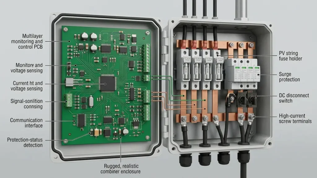
PV combiner box PCB monitoring board separated from the main DC power path with busbars and fuses
One of the most important issues during OEM procurement is defining exactly what the PCB is expected to do.
A monitoring and control PCB has different electrical and manufacturing requirements from a board or conductor structure intended to carry substantial DC current. Treating these functions as interchangeable can lead to incorrect material selection, unsuitable copper design, and incomplete safety reviews.
Monitoring and Control Circuit Boards
A PV combiner box monitoring PCB may include:
- Analog signal-conditioning circuits
- Current and voltage measurement interfaces
- MCU and communication circuits
- Temperature-sensor interfaces
- Protection-status detection circuits
- Auxiliary power regulation
- Signal connectors and control interfaces
The board’s layer count, copper thickness, material, insulation structure, and component layout should be selected according to the actual circuit and operating environment.
For designs involving isolated measurement, the isolation components and PCB layout must be considered together. The PCB fabricator should receive the relevant schematic, stack-up requirements, and layout data to assess manufacturability.
Busbars, Fuses, SPDs and DC Disconnects
The main DC power path is generally designed around components and conductors selected for the system’s voltage, current, fault conditions, and applicable safety requirements.
These may include:
- Copper busbars and power terminals
- PV-rated fuse links and fuse holders
- Surge protection devices
- DC disconnect switches
- High-current cables and connectors
A monitoring PCB may connect to these devices through measurement or status interfaces, but that does not mean the PCB itself carries the full string current.
For procurement purposes, OEM buyers should identify which components are mounted on the PCB, which are connected externally, and which belong to the enclosure’s main power assembly.
PCB Integration Requirements
The PCB’s mechanical and electrical interfaces should be reviewed against the complete combiner box assembly.
Important details include:
- Board outline and mounting-hole positions
- Connector orientation and terminal accessibility
- Component height and enclosure clearance
- Creepage and clearance requirements
- Insulation barriers and isolation slots, where required
- Heat sources near sensitive components
- Cable entry and wiring access
- Environmental sealing and condensation considerations
A board can meet its individual fabrication tolerances and still create integration problems if connector access, enclosure dimensions, or wiring arrangements have not been checked.
Key Engineering Requirements for PV Combiner Box PCBs
PV combiner box PCB requirements vary with system voltage, grounding arrangement, number of strings, monitoring architecture, installation environment, and applicable product standards. There is no single PCB specification that is suitable for every 1000V or 1500V DC application.
1000V and 1500V DC System Considerations
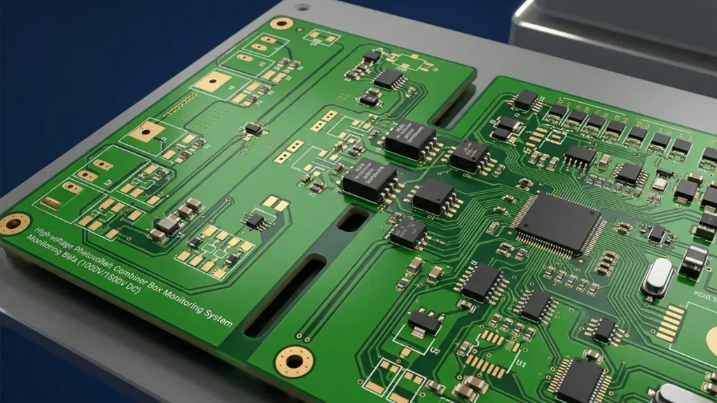
PV combiner box PCB design for 1000V and 1500V DC systems showing electrical isolation and creepage clearance spacing
The nominal DC system voltage is an important input for the electrical design review. However, it is not sufficient on its own to determine PCB insulation spacing or construction.
Before manufacturing, the OEM engineering team should provide:
- Maximum operating voltage
- System grounding arrangement
- Expected transient and overvoltage conditions
- Applicable product and safety standards
- Pollution degree and installation environment
- Operating altitude, where relevant
- Insulation coordination requirements
- Whether measurement circuits are isolated or non-isolated
A 1500V DC system does not automatically mean that every circuit on its monitoring PCB operates at 1500V. Some circuits may operate at low voltage, while sensing interfaces may be exposed to high common-mode voltage or require defined isolation barriers.
This distinction should be reflected in the schematic, PCB layout, component ratings, and manufacturing documentation.
Creepage, Clearance and Electrical Isolation
Creepage and clearance are two separate considerations in high-voltage PCB design.
- Clearance is the shortest distance through air between conductive parts.
- Creepage is the shortest distance along an insulating surface between conductive parts.
The required distances depend on the applicable safety standard and design conditions. Relevant factors may include working voltage, impulse voltage, pollution degree, material group or CTI, insulation category, and altitude.
PCB layout features such as slots, routing channels, component spacing, and isolation barriers may help meet the design requirements, but they must be evaluated as part of the complete insulation system.
For OEM procurement, the buyer should provide the required spacing rules or the applicable design standard. A PCB supplier should not apply one generic clearance value to every 1000V or 1500V DC project.
Current Sensing and Signal Conditioning
Current measurement accuracy can be affected by several factors:
- Sensor selection and measurement topology
- Shunt resistor tolerance and temperature coefficient
- Hall-effect sensor characteristics, where used
- PCB copper resistance and thermal behavior
- Analog front-end layout
- Grounding and common-mode voltage
- Calibration and production test procedures
For shunt-based designs, the Kelvin connection arrangement and routing symmetry may be important. For isolated sensing, the isolation component, power supply, signal path, and PCB spacing need to be reviewed together.
OEM buyers should define the measurement range, target accuracy, calibration requirements, and operating temperature range in the technical specification.
RS-485 and Modbus Communication
RS-485 is commonly considered for industrial communication between monitoring electronics and external control equipment. Where Modbus RTU is used, the PCB design must support the required transceiver, protection components, termination arrangement, and connector interface.
The design review should cover:
- Differential pair routing and signal reference
- Cable and connector specifications
- Surge and ESD protection requirements
- Bus termination and biasing
- Grounding and isolation architecture
- Communication test conditions
Modbus RTU is a communication protocol, not a PCB manufacturing specification. The exact protocol configuration and test cases should be supplied by the customer or agreed during engineering review.
Thermal Management and Component Reliability
PV combiner boxes may operate in outdoor environments exposed to elevated ambient temperatures, solar radiation, humidity, and temperature cycling.
These conditions can affect electronic components, solder joints, connectors, and PCB materials.
Engineering review should consider:
- Component temperature ratings and derating
- Heat generated by power-related components
- Distance between heat sources and measurement circuits
- Copper distribution and local thermal concentration
- Connector and solder-joint reliability
- Moisture exposure and condensation risks
- Enclosure ventilation and thermal design
Fuse and terminal overheating are system-level concerns. They can result from contact resistance, incorrect installation torque, unsuitable component selection, excessive current, or other design and assembly issues. They should not automatically be attributed to the PCB.
Where thermal verification is required, the OEM should define the test conditions, measurement locations, operating load, and acceptance criteria.
Custom PV Combiner Box PCB Manufacturing
A custom PV combiner box PCB should be manufactured according to the released design files and the electrical and mechanical requirements of the project.
The correct material and construction depend on the board’s operating conditions, circuit function, component density, thermal environment, and reliability targets.
PCB Materials and Layer Configuration
FR-4 is commonly used for control and monitoring electronics, but the final material selection should be based on the actual application requirements.
The engineering review may include:
- Base material and specified grade
- Number of copper layers
- Finished board thickness
- Copper thickness
- Glass transition temperature (Tg), where specified
- Dielectric properties, where relevant
- Solder mask and surface finish
- Board dimensional and mechanical requirements
A higher layer count is not automatically better. The stack-up should support the routing, grounding, signal integrity, insulation, and mechanical requirements of the design.
Copper Thickness and Trace Design
Copper thickness and trace geometry should be selected according to the current carried by each circuit, allowable temperature rise, voltage drop, and manufacturing tolerances.
For monitoring boards, low-level measurement signals and power supply circuits may have very different copper requirements. If the PCB includes higher-current paths, those areas need separate electrical and thermal evaluation.
The fabrication review should check:
- Finished copper thickness
- Minimum trace width and spacing
- Annular ring and via requirements
- Plated through-hole reliability
- Copper balance and layer distribution
- Solderability and surface finish
The final values should follow the approved Gerber or ODB++ data and the customer’s specification rather than a generic PV combiner box template.
PCB Fabrication and DFM Review
Before production, a design-for-manufacturing (DFM) review can identify potential fabrication issues.
Typical review items include:
- Minimum trace width and spacing
- Drill size and aspect ratio
- Copper-to-edge clearance
- Solder mask openings
- Via and annular ring design
- Board thickness and tolerance
- Layer registration
- Impedance requirements, if applicable
- Panelization and tooling considerations
PCBKR’s manufacturing information includes precision imaging, laser drilling, multilayer lamination, and inspection processes. For example, the stated LDI process target is 8 μm with ±10 μm tolerance, while laser drilling capabilities vary by process and feature specification. Final feasibility must be confirmed against the actual production data and board construction.
PCB Specifications Based on Gerber Files
For an accurate PV combiner box PCB quotation, the buyer should provide the released design data rather than relying only on a product name.
The quotation review may cover:
| Specification | Information to Confirm |
|---|---|
| Base material | FR-4 grade or customer-specified material |
| Layer count | Actual copper layer configuration |
| Board thickness | Finished thickness and tolerance |
| Copper thickness | Starting and finished copper requirements |
| Minimum trace/space | Design minimums and fabrication requirements |
| Minimum hole | Finished hole and drill requirements |
| Surface finish | ENIG, lead-free HASL, or other specified finish |
| Solder mask | Color and defined coverage requirements |
| Special requirements | Impedance, insulation, testing, or reliability criteria |
These are project-dependent parameters, not universal PV combiner box PCB specifications.
PV Combiner Box PCBA Assembly Services
For OEM manufacturers, sourcing PCB fabrication and assembly through one supplier can simplify production coordination, provided the supplier can support the required components, assembly processes, and quality controls.
PCBKR provides PCB manufacturing and PCBA assembly services. The exact assembly scope should be confirmed from the customer’s BOM, assembly drawings, and project requirements.
SMT and Through-Hole Assembly
A PV combiner box control or monitoring board may combine surface-mount and through-hole components.
Typical assembly considerations include:
- MCU and signal-processing ICs
- Measurement and interface components
- Power-management devices
- Connectors and terminal blocks
- Relays or other customer-specified components
- Through-hole components requiring mechanical retention
The assembly process should be selected according to component packages, board thickness, soldering requirements, and the expected operating environment.
Component Sourcing and BOM Management
Component availability can affect both prototype schedules and long-term production costs.
Before procurement, the BOM should be reviewed for:
- Manufacturer part numbers
- Approved manufacturers and alternatives
- Package and footprint consistency
- Operating temperature ratings
- Voltage and current ratings
- Lifecycle and availability risks
- Customer-controlled or supplied components
Substitutions should not be made solely because a component has a similar package or nominal electrical value. Any proposed alternative should be reviewed against the circuit function and approved by the customer.
Mixed Technology Assembly
Some PV combiner box boards require both SMT and through-hole assembly. The assembly sequence and process controls should account for component placement, soldering method, connector alignment, and mechanical stress.
For boards with large connectors or components subject to cable forces, the mechanical interface and solder-joint design should be reviewed before production.
Prototype and Mass Production
Prototype production helps verify the board’s electrical function, assembly feasibility, and mechanical integration before volume manufacturing.
A practical OEM production process includes:
- Review Gerber or ODB++ files and BOM.
- Confirm PCB construction and assembly requirements.
- Review component availability and approved alternatives.
- Manufacture prototype PCBs and assemble samples.
- Complete customer-defined inspection and functional verification.
- Obtain sample approval and release production documentation.
- Proceed with pilot or volume production under the approved specification.
The prototype stage should be used to resolve design and assembly issues, not simply to confirm that the board can be manufactured.
Quality Inspection and Testing for PV Combiner Box PCBA
Inspection and testing requirements should be defined according to the board’s function and the customer’s quality plan. Visual inspection alone is not sufficient for every monitoring or control board.
AOI and X-ray Inspection
Automated Optical Inspection (AOI) can help identify assembly defects such as component placement errors, soldering issues, and polarity problems.
X-ray inspection may be appropriate for hidden solder joints, including selected BGA and other bottom-terminated packages.
The inspection method should be chosen according to the actual component packages and assembly risks.
Electrical Testing
Electrical testing may include continuity, short-circuit, and other board-level checks defined by the design and test specification.
For bare PCB production, the required electrical test method should be agreed according to the board design and order requirements. For assembled boards, the test plan should identify the test points, expected values, and acceptance limits.
PCBKR’s stated inspection resources include flying probe testing and four-wire Kelvin measurement. Whether a particular method is suitable depends on the PCB design and the required test coverage.
Communication and Functional Testing
A PV combiner box PCBA may require functional verification of measurement channels, communication interfaces, and status-detection circuits.
A customer-defined test fixture may be used to verify functions such as:
- Voltage measurement response
- Current measurement response
- Temperature sensor input
- Fuse or SPD status signal detection
- RS-485 communication
- MCU operation and firmware loading
- Alarm or output signal behavior
These tests require agreed test procedures, firmware, fixtures, input conditions, and acceptance limits. They should be included in the quotation scope rather than assumed to be part of every standard assembly order.
Project-Specific Reliability Verification
Some OEM projects may require additional verification, such as temperature cycling, humidity exposure, vibration, or other environmental testing.
The required test method and acceptance criteria should be based on the product’s intended application and applicable standards. A PCB assembly supplier should distinguish between routine production inspection and additional qualification testing.
OEM Procurement: From Gerber and BOM to Production
A clear RFQ package helps PCB and PCBA suppliers evaluate the project accurately and reduces avoidable delays during quotation and engineering review.
Required Files for RFQ
For a PV combiner box PCB or PCBA quotation, buyers should prepare:
| Required Information | Purpose |
|---|---|
| Gerber or ODB++ files | PCB fabrication review |
| PCB stack-up | Layer construction and material confirmation |
| BOM | Component sourcing and assembly quotation |
| Centroid / pick-and-place file | SMT placement data |
| Assembly drawings | Component orientation and assembly details |
| PCB specifications | Thickness, copper, finish, tolerances |
| Electrical requirements | Voltage, current, sensing range, and interfaces |
| Testing requirements | Inspection, electrical, and functional test scope |
| Estimated quantity | Prototype, pilot, and mass production planning |
| Delivery requirements | Target lead time and shipping arrangements |
If the project includes firmware programming, functional testing, or special inspection, those requirements should be stated in the RFQ.
DFM and BOM Review
After receiving the files, the supplier should review the PCB construction and assembly data for manufacturability.
The review should identify potential issues such as:
- Fabrication features outside the agreed process capability
- Missing or inconsistent stack-up information
- BOM part-number or footprint mismatches
- Unavailable or obsolete components
- Unclear polarity or orientation
- Incomplete test-point access
- Connector or enclosure integration conflicts
Any proposed changes should be documented and approved before production.
Prototype Approval
The prototype stage provides an opportunity to verify the manufactured board against the released design.
OEM buyers should review:
- PCB dimensions and construction
- Component placement and assembly quality
- Electrical test results
- Functional test results, where included
- Mechanical fit and connector access
- Any deviations from the approved specification
Once the sample is approved, the released files and revision status should be controlled for subsequent production.
Volume Production and Delivery
For repeat orders, production consistency depends on maintaining controlled design revisions, approved BOM data, manufacturing instructions, and inspection criteria.
Before placing a volume order, buyers should confirm:
- Approved PCB and PCBA revisions
- Component sourcing arrangements
- Production quantity and delivery schedule
- Inspection and test records required
- Packaging and traceability requirements
- Change-control and deviation-approval procedures
These controls help OEM manufacturers maintain consistency between prototype, pilot production, and recurring supply.
Why Choose PCBKR for PV Combiner Box PCB Manufacturing?
Shenzhen Hongda Circuit Technology Co., Ltd. (PCBKR) provides PCB manufacturing and PCBA assembly services for customers developing electronic control, monitoring, and power-related products.
For PV combiner box OEM projects, the manufacturing scope can be evaluated according to the customer’s released design files and required production process.
Relevant manufacturing and inspection resources include:
- Precision PCB imaging and multilayer fabrication processes
- Laser drilling processes for specified hole and via requirements
- PCB fabrication inspection
- AOI and X-ray inspection for applicable assembly requirements
- Flying probe and four-wire Kelvin testing resources
- PCB fabrication and PCBA assembly coordination
The final process selection depends on the actual board design, component package, quantity, and quality requirements. High-voltage insulation design, system-level certification, and complete combiner box qualification must be addressed within the appropriate product engineering and certification scope; they should not be inferred from PCB fabrication capability alone.
If your project also includes embedded monitoring or control electronics, see PCBKR’s Embedded Control Board OEM Manufacturing service. For boards requiring an auxiliary power conversion stage, review the PCB for Power Supply manufacturing page.
PCBKR can review your Gerber files, BOM, PCB specifications, and assembly requirements to evaluate the manufacturing scope for prototype and production orders.
Frequently Asked Questions About PV Combiner Box PCB Suppliers
How Do I Choose a PV Combiner Box PCB Manufacturer?
Choose a manufacturer that can review your Gerber files, PCB stack-up, BOM, assembly drawings, and testing requirements before quotation. Evaluate its PCB fabrication processes, PCBA assembly capability, inspection resources, engineering communication, and ability to support repeat production. For high-voltage applications, make sure the insulation and safety requirements are clearly defined by the product design team.
Can a PCB Manufacturer Produce Custom PV Combiner Box PCBs from Gerber Files?
Yes. A PCB manufacturer can evaluate custom PV combiner box PCB designs from Gerber or ODB++ files, together with the stack-up and fabrication specifications. The supplier should review layer count, board thickness, copper weight, trace and spacing requirements, drill sizes, surface finish, and any special electrical or mechanical requirements before confirming manufacturability and price.
Can One Supplier Provide Both PV Combiner Box PCB Fabrication and PCBA Assembly?
A supplier offering both PCB fabrication and PCBA assembly can coordinate bare-board production, component sourcing, SMT or through-hole assembly, and agreed inspection processes. Buyers should confirm whether the quotation covers PCB fabrication only, assembly only, or a complete turnkey PCBA scope, including component procurement and functional testing.
What PCB Requirements Should I Provide for a 1000V or 1500V PV Combiner Box?
Provide the maximum system voltage, grounding arrangement, circuit schematic, isolation architecture, applicable safety standards, pollution degree, operating altitude where relevant, and required insulation criteria. The PCB’s creepage and clearance requirements must be evaluated according to the actual design conditions and applicable standards. A nominal voltage value alone is not enough to establish the required spacing.
What Documents Are Needed to Get a PV Combiner Box PCBA Quote?
For an accurate quotation, provide Gerber or ODB++ files, PCB stack-up, BOM with manufacturer part numbers, pick-and-place data, assembly drawings, PCB specifications, estimated order quantity, and delivery requirements. If functional testing, firmware programming, or special reliability verification is required, include the test procedure and acceptance criteria in the RFQ.
Request a PV Combiner Box PCB & PCBA Quote
Are you developing a PV combiner box monitoring board, string measurement PCB, or protection-status control PCBA?
Send PCBKR your Gerber or ODB++ files, BOM, board specifications, and estimated production quantity. Our team can review the manufacturing and assembly requirements and provide a project-based quotation.
Shenzhen Hongda Circuit Technology Co., Ltd. (PCBKR)
Email: sales@pcbkr.com
Website: www.pcbkr.com
Request a PCB & PCBA Quote.
About Author
David Chen LinkedIn Profile
David Chen is a Senior RF/PCB Process Engineer at Shenzhen Hongda Circuit Technology Co., Ltd., with over 12 years of experience in high-frequency PCB fabrication, impedance-controlled stack-up design, and Rogers/PTFE laminate processing. He also boasts an extensive professional background in PCBA manufacturing, PCBA testing, and PCBA optimization, with specialized expertise in high-precision PCBA fault analysis and rigorous PCBA reliability testing. The author has worked with high-layer-count server PCB fabrication, ultra-low-loss backplane stackups, and thermo-mechanical reliability optimization for AI infrastructure projects involving 112G and 224G PAM4 architectures. Skilled in complex circuit design and cutting-edge advanced PCB manufacturing processes, he delivers solutions that elevate product durability and performance across industrial applications. His technical articles focusing on PCBA manufacturing workflows and testing methodologies are widely cited by industry peers and technical platforms, and have gained attention and recognition from industry colleagues.