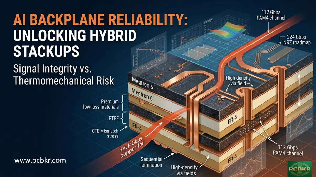
How Hybrid Stackups Affect AI Backplane Reliability
Hybrid stackups — combining low-loss laminates (PPE/PPO-based Megtron 6, or true PTFE) with FR-4 — improve 112 Gbps+ AI backplane signal integrity but introduce CTE-mismatch delamination risk up to 40% higher than all-FR-4 builds. Copper foil roughness and fiber weave effects further complicate reliability. Correct material classification, sequential lamination planning, and per-layer simulation are mandatory for any qualified AI server PCB manufacturer.
Why Do AI Server PCB Manufacturers Need Hybrid Stackups for Backplane Designs?
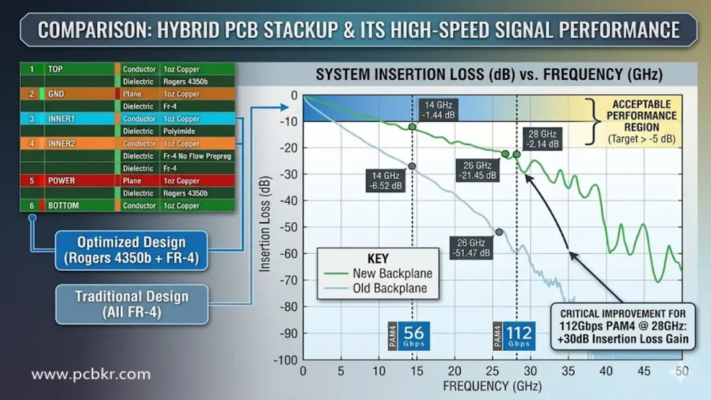
omparison: Hybrid PCB Stackup & High-Speed Insertion Loss Performance
Modern AI training clusters operate backplanes at 112 Gbps PAM4 per lane, with roadmaps targeting 224 Gbps NRZ by 2026. At these speeds, the dielectric loss tangent (Df) of conventional FR-4 (Df approximately 0.020 to 0.025 at 10 GHz) exceeds acceptable insertion-loss budgets. For a 600 mm backplane trace running at 28 GHz Nyquist (the Nyquist frequency for 112 Gbps PAM4), an all-FR-4 construction accumulates roughly -8 to -10 dB of insertion loss — well beyond the -6 dB channel budget defined by OIF-CEI-112G-LR at 28 GHz.
0.004
Loss Tangent (Df)
Isola Tachyon 100G at 10 GHz, vs. FR-4 typical of 0.022
-6 dB
@ 28 GHz
OIF-CEI-112G-LR insertion loss budget limit for 600 mm AI backplane channel
112+
Gbps / lane
Current target lane rate for PCIe 6.0 / OIF-CEI-112G in AI backplanes
3-5x
Cost Premium
PTFE or PPE/PPO laminates vs. standard FR-4, driving selective hybrid designs
Because full-board exotic laminate would cost $4,000 to $8,000 per square foot in volume production (IPC-2581 cost benchmarks, 2024), qualified AI server PCB manufacturers selectively apply low-loss materials to high-speed signal layers while retaining FR-4 for power distribution and structural layers — the hybrid stackup strategy.
What Are the Two Fundamentally Different Types of Hybrid Stackup Used in AI Backplanes?
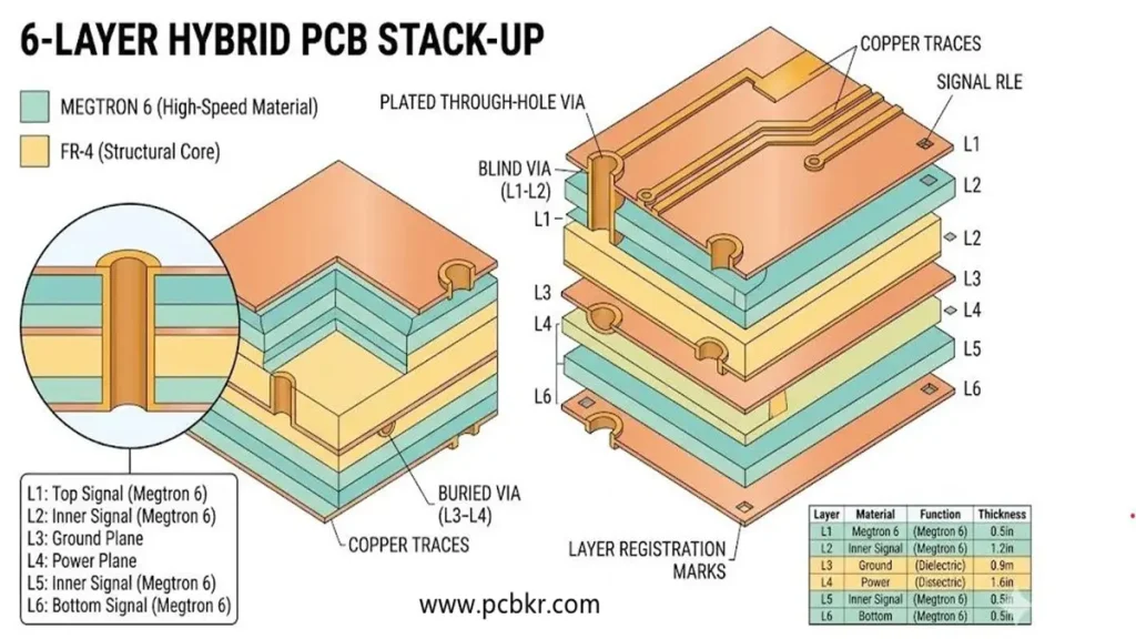
6-Layer Hybrid PCB Stack-up Diagram (Megtron 6 + FR-4)
A persistent industry error — and a critical design risk — is treating all hybrid stackups as equivalent. In practice, an experienced AI server PCB manufacturer must distinguish between two combinations that have completely different lamination processes, bonding chemistry, and reliability profiles:
Common Misconception Corrected: Rogers RO4003C is NOT a PTFE material. It is a hydrocarbon/ceramic (HC/Ce) laminate processed at standard FR-4-compatible temperatures (~180 degrees C). It does not require plasma etch or sodium-naphthalene surface activation. Classifying RO4003C as PTFE in a stackup specification will cause your fabricator to apply incorrect surface treatment and bonding chemistry.
| Hybrid Type | Example Materials | Lamination Temp | Surface Prep Required | Fab Complexity |
|---|---|---|---|---|
| FR-4 + PPE/PPO | Isola 370HR + Panasonic Megtron 6 (R-5775) | 175 to 185 degrees C | Standard oxide or micro-etch; no special activation | MODERATE |
| FR-4 + HC/Ce | Isola 370HR + Rogers RO4003C / RO4350B | 170 to 180 degrees C | Standard oxide treatment; FR-4-compatible processing | LOW-MOD |
| FR-4 + PTFE (true fluoropolymer) | Isola 370HR + Rogers RT/duroid 5880, Taconic TLY | 300 degrees C+ for PTFE layers | Plasma etch or sodium naphthalene activation mandatory; peel strength target above 0.7 N/mm | HIGH — requires sequential lamination |
The FR-4 + PPE/PPO combination (e.g., FR-4 with Megtron 6) is the dominant choice for production AI server backplanes today. The cure temperatures are close enough to permit single-stage lamination with a compatible transition prepreg such as Panasonic R-5575(N). True PTFE hybrids, by contrast, require sequential lamination — a two-stage press cycle that significantly increases cycle time, warpage risk, and per-board cost.
How Do Copper Foil Roughness and Fiber Weave Effects Impact Hybrid Backplane Signal Integrity at 224 Gbps?
Most published hybrid stackup guides focus exclusively on dielectric loss (Dk/Df). At 112 Gbps PAM4 and especially at 224 Gbps NRZ, two additional loss mechanisms become equally or more significant: conductor loss driven by copper foil surface roughness, and differential skew caused by fiber weave periodicity.
Why Does Copper Foil Profile Matter to an AI Server PCB Manufacturer?
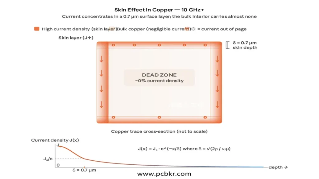
High-Frequency Signal Attenuation: Copper Skin Depth Diagram
At frequencies above 1 GHz, signal current flows only in a thin skin at the copper surface (skin depth at 10 GHz is approximately 0.7 micrometers). A standard electrodeposited (ED) copper foil has an Rz surface roughness of 5 to 8 micrometers — 7 to 11 times the skin depth at 10 GHz. This creates the Hammerstad-Jensen roughness correction: effective conductor loss increases by a factor of 1.5x to 2.5x versus smooth-copper models at 28 GHz Nyquist.
2.5x higher
Conductor loss multiplier for standard ED copper (Rz = 6 micrometers) vs. theoretical smooth copper at 28 GHz, per Hammerstad-Jensen model. HVLP (High Very Low Profile) foil with Rz below 2 micrometers reduces this factor to approximately 1.3x.
Source: Hammerstad and Jensen, “Accurate Models for Microstrip Computer-Aided Design,” IEEE MTT-S 1980; validated in Isola application note “Copper Foil Selection for 112G Channels,” 2023
The critical reliability complication for hybrid stackups: HVLP and Ultra-Low Profile (ULP) copper foils have significantly lower peel strength than standard ED copper — typically 0.5 to 0.7 N/mm versus 0.9 to 1.2 N/mm for standard ED. When combined with the already-reduced adhesion at a PTFE or PPE/FR-4 material interface, using HVLP foil can push peel strength below IPC-4101E Class C minimums, increasing delamination risk at the exact layers where SI demands low-roughness copper.
At 224 Gbps NRZ (Nyquist 56 to 112 GHz), this constraint becomes even more acute. Traditional chemical micro-etch — which roughens the base laminate surface to improve mechanical interlocking with copper — cannot be used with HVLP foil because any surface roughening of the laminate undermines the smooth Dk uniformity the foil was selected to preserve. Leading AI server PCB manufacturers instead qualify silane coupling agent (SCA) surface treatments or proprietary molecular bonding systems (such as MacDermid Alpha’s Multibond or Atotech’s Bondfilm) that achieve adequate adhesion through chemical bonding at the molecular level rather than mechanical interlocking. Specifying the bonding process by name — not just “HVLP foil with standard oxide” — in the fabrication drawing notes is critical to ensuring the correct process is applied in production.
Does Fiber Weave Effect Become a Reliability Issue in Hybrid Stackups?
In 48-layer AI backplanes operating at 112 Gbps PAM4, intra-pair skew caused by fiber weave periodicity is a channel compliance failure mode — not just a signal integrity annoyance. Standard woven glass fabric (e.g., 2116 style) has a periodic Dk variation of plus or minus 0.3 to 0.5 due to alternating resin-rich and glass-rich zones. For a 100 mm differential pair trace, this can produce 5 to 15 ps of intra-pair skew — exceeding the 10 ps budget in many 112G specifications.
The solution used by leading AI server PCB manufacturers is spread-glass (flat-weave) reinforcement fabric: styles 1067, 1078, and 106 with spread-glass treatment. These reduce Dk periodicity variation to below plus or minus 0.1, cutting fiber-weave-induced skew by 60 to 80%. Specifying spread-glass fabric should be a mandatory requirement in the PCB stackup document for any AI backplane operating above 56 Gbps.
Which Thermomechanical Failure Modes Are Amplified in Hybrid Stackups for AI Infrastructure?
Signal integrity improvements introduce a reliability trade-off: CTE mismatch between laminate materials generates interfacial stress during thermal cycling. AI backplanes in data center environments experience 500 to 2,000 thermal cycles annually (ASHRAE A1-class guidelines), driven by inlet air temperature fluctuations and planned maintenance events.
| Material | Resin System | CTE x/y (ppm/C) | CTE z (ppm/C) | Fab Risk at Interface |
|---|---|---|---|---|
| FR-4 (Isola 370HR) | Epoxy | 14 to 17 | 55 to 70 | BASELINE |
| Megtron 6 (R-5775) | PPE/PPO | 13 to 14 | 40 to 45 | LOW |
| Rogers RO4003C | HC/Ceramic (NOT PTFE) | 11 to 13 | 46 to 50 | LOW-MOD — FR-4-compatible process |
| Isola Tachyon 100G | Modified PPE | 11 to 13 | 28 to 35 | MODERATE at boundaries |
| Rogers RT/duroid 5880 | True PTFE + glass | 31 to 35 ⚠ X/Y CTE exceeds FR-4 baseline (14-17) — see note below | 24 to 28 | HIGH — sequential lamination + registration control required |
Engineering Note — RT/duroid 5880 CTE Anomaly: Unlike glass-reinforced epoxy laminates where woven glass constrains x/y expansion well below z-axis values, PTFE-based materials reinforced with woven glass can exhibit anomalously high x/y CTE (31 to 35 ppm/C) due to the high Poisson’s ratio and viscoelastic behavior of the PTFE matrix above its glass transition. This means the x/y expansion of RT/duroid 5880 (31-35) is roughly 2x that of FR-4 (14-17). In a hybrid stackup, this mismatch generates severe in-plane shear stress at material boundaries during thermal cycling, causing layer-to-layer registration deviation (pattern-to-pattern misalignment) in addition to z-axis delamination risk. For high-density via fields in 48-layer AI backplanes, this registration shift can collapse via-to-pad annular ring and cause open-circuit failures that are not detectable by standard electrical test.
Can Delamination Risk Be Quantified for Mixed-Material Interfaces?
IPC-TM-650 Method 2.4.8 thermal shock testing (-55 degrees C to +125 degrees C, 100-cycle ramp) of hybrid PTFE/FR-4 coupons without surface treatment shows delamination onset at the material boundary at approximately 60 to 70 cycles — versus 200+ cycles for all-FR-4 boards. Plasma-etch surface treatment of true PTFE layers before lay-up extends first-delamination onset to 160+ cycles. FR-4 + Megtron 6 hybrids with compatible transition prepreg pass 500+ cycles without delamination in the same test protocol.
40% higher
Delamination rate at untreated PTFE-to-FR-4 bond interfaces vs. homogeneous FR-4 boards under IPC-TM-650 2.4.8 thermal shock (100 cycles, -55 to +125 degrees C). FR-4 + PPE/PPO (Megtron 6) hybrids with R-5575(N) transition prepreg do not show this elevation.
Source: IPC White Paper IPC-WP-019, “Reliability of Mixed-Material PCB Constructions,” 2023; TTM Technologies failure analysis report, Q2 2024
How Does Sequential vs. Single-Stage Lamination Affect Warpage in 48-Layer AI Backplanes?
This is the manufacturing pain point most articles omit. FR-4 and true PTFE cure at temperatures 120 degrees C apart. A single-stage press cycle cannot provide the correct thermal profile for both materials simultaneously: under-curing the FR-4 layers reduces Tg and z-axis CTE performance; over-cycling degrades PTFE layer adhesion and increases resin bleed (flow loss). The result is unacceptable thickness tolerance — typically plus or minus 8% on overall board thickness versus the target plus or minus 4% — and warpage that can exceed 0.75% bow/twist, making SMT placement impossible for BGA components.
Sequential lamination (press PTFE sub-laminate first at 300+ degrees C, then co-laminate with FR-4 at 180 degrees C in a second press cycle) solves the thermal profile conflict but adds 30 to 40% to fabrication cycle time and introduces new registration challenges at the sub-laminate boundary. Any AI server PCB manufacturer quoting true PTFE hybrid backplanes should be required to provide warpage data from at least three production lots before qualification.
What Design and Fabrication Rules Should AI Server PCB Manufacturers Follow for Hybrid Backplane Reliability?
How Should Layer Assignment Be Determined for a 48-Layer AI Backplane?
Run full channel loss budget simulation (Ansys SIwave or Cadence Sigrity) with layer-specific Dk/Df and copper foil roughness parameters. Apply low-loss laminate only to layers where insertion loss exceeds -1 dB per 100 mm at the Nyquist frequency of your target data rate. A typical 48-layer AI backplane requires premium material on only 8 to 12 layers, reducing cost 55 to 65% versus full-board exotic laminate while achieving the same channel compliance.
- Specify HVLP or ULP copper foil (Rz below 2 micrometers) on all premium-laminate high-speed layers — and validate peel strength meets IPC-4101E Class C (above 0.7 N/mm) with the specific laminate and foil combination
- Specify spread-glass fabric (style 1067, 1078, or 106) on all signal layers operating above 56 Gbps to limit fiber-weave skew below 10 ps per 100 mm
- For FR-4 + Megtron 6 (PPE/PPO) hybrids: use Panasonic R-5575(N) transition prepreg at all material boundaries; single-stage lamination at 180 degrees C is acceptable
- For FR-4 + true PTFE hybrids: plasma-etch or sodium-naphthalene surface activation of PTFE layers is mandatory; plan for sequential lamination (two press cycles); request warpage data from at least three lots
- Run 3D full-wave simulation (Ansys HFSS or Keysight EMPro) for every material interface via — 2D solvers are insufficient above 25 GHz because they cannot resolve field discontinuity at dielectric boundaries
- Back-drill all through-hole vias to stub length below 0.25 mm for channels above 28 GHz Nyquist; note that stub resonance frequency shifts with local Dk at the material boundary and must be re-simulated per layer
- Validate final build with cross-section coupon at each material interface on every production lot — at designated hybrid-zone coupon locations on the panel edge, not only corner-of-board standard locations; this requirement must be written into the Quality Control Plan (IPC-6012 Class 3 Section 3.7)
“Hybrid laminate interfaces are the new SI battleground. Every material boundary is a potential return-loss event that pre-layout simulation must model explicitly — bulk-property assumptions fail above 25 GHz.”– Eric Bogatin, Signal Integrity Journal, “Hybrid Stackups in 112G Designs,” Vol. 12, 2024
How Do Testing and Qualification Protocols Need to Change for Hybrid AI Backplanes?
Standard IPC Class 3 qualification was designed for homogeneous FR-4. Hybrid stackups for AI server PCB manufacturing require additional protocol steps at every production stage:
C-SAM
Acoustic Microscopy
Detects sub-surface delamination at material interfaces before and after thermal cycling — required for all hybrid configurations
TDR
Time-Domain Reflectometry
Measures impedance profile across material transitions on every production board; tolerance plus or minus 5 Ohm per IPC-2141C
IST
Interconnect Stress Test
IPC-TM-650 2.6.26: accelerated thermal cycling; acceptance criterion: less than 10% barrel resistance increase at 500 cycles
VNA
S-Parameter Sweep
Full 4-port S-parameter characterization to 67 GHz (or 110 GHz for 224G channels) on channel coupon per production lot
The IPC-2591 (Connected Factory Exchange) initiative now includes hybrid stackup qualification data exchange formats, enabling fab-to-OEM traceability of material boundary locations and test results — a critical capability for AI hyperscaler supply chains managing hundreds of board variants simultaneously.
Frequently Asked Questions
Is Rogers RO4003C a PTFE laminate, and does it need plasma etch surface treatment in a hybrid stackup?
No — Rogers RO4003C is a hydrocarbon/ceramic (HC/Ce) laminate, not PTFE, and does not require plasma etch or sodium-naphthalene surface activation. This is one of the most common material misclassifications in hybrid stackup specifications. RO4003C processes at standard FR-4-compatible temperatures (approximately 175 to 180 degrees C) and bonds to FR-4 prepreg with standard oxide or micro-etch treatment. Applying PTFE surface activation chemistry to RO4003C will degrade the copper-laminate bond. True PTFE materials — such as Rogers RT/duroid 5880 or Taconic TLY series — do require plasma or chemical activation. Always verify resin system (not just trade name) before specifying surface treatment in a hybrid stackup fab note. (Source: Rogers Corporation RO4000 Series Laminate Data Sheet, Rev. 2024; IPC-4101E Material Classification)
Why does copper foil roughness matter in hybrid stackup selection for AI server PCB manufacturing?
Copper foil surface roughness is often the dominant loss mechanism above 10 GHz, and the foil type directly affects bond reliability at hybrid laminate interfaces. At 28 GHz (Nyquist for 112 Gbps PAM4), standard ED copper (Rz approximately 6 micrometers) increases effective conductor loss by up to 2.5x versus a smooth-copper theoretical model. Using HVLP foil (Rz below 2 micrometers) reduces this to approximately 1.3x. However, HVLP foil has lower peel strength (0.5 to 0.7 N/mm vs. 0.9 to 1.2 N/mm for standard ED). In a hybrid stackup, this reduced peel strength at a PTFE or PPE/FR-4 boundary can push the interface below IPC-4101E Class C minimums. The design solution is to validate HVLP foil peel strength on actual hybrid layer-pair test coupons before committing to production — not on single-material test boards. (Source: Isola Application Note, “Copper Foil Selection for 112G Channels,” 2023; IPC-4101E)
What hybrid stackup combination do qualified AI server PCB manufacturers most commonly use in production today?
FR-4 (Isola 370HR or equivalent) combined with Panasonic Megtron 6 (PPE/PPO resin) is the dominant production choice for AI backplanes at 112 Gbps PAM4. This combination permits single-stage lamination at approximately 180 degrees C with Panasonic R-5575(N) transition prepreg, eliminating the sequential lamination complexity of true PTFE hybrids. Meta’s Open Compute Project AI/HPC backplane specification v2.1 (2024) documents a 48-layer FR-4 + Megtron 6 construction validated to 1,000-cycle accelerated life test. True PTFE hybrids are reserved for extreme-performance applications (224 Gbps NRZ, mmWave radar, aerospace) where the fabrication complexity is justified by channel performance requirements that PPE-class laminates cannot satisfy.
Fiber weave periodicity causes intra-pair skew of 5 to 15 ps per 100 mm, which can exceed the 10 ps differential skew budget in 112G specifications — a direct compliance failure. Standard woven glass (e.g., 2116 style) alternates resin-rich and glass-rich zones with a Dk variation of plus or minus 0.3 to 0.5. When one trace in a differential pair runs over glass bundles and its companion runs over resin pockets, propagation velocity differs, producing skew. The solution adopted by leading AI server PCB manufacturers is mandatory use of spread-glass (flat-weave) fabric styles 1067, 1078, or 106 — which reduce Dk periodicity variation to below plus or minus 0.1 and cut fiber-weave skew by 60 to 80%. This fabric specification must appear in the PCB procurement document, not left to the fabricator’s discretion. (Source: IPC-2141C; Panasonic Megtron 6 Application Guide, 2024)
Sequential lamination for true PTFE hybrids introduces 30 to 40% longer cycle time and warpage risk that can push bow/twist beyond 0.75%, making SMT placement of BGA components impossible. The 120 degrees C cure-temperature gap between FR-4 and PTFE makes single-stage lamination thermally incompatible: under-curing the FR-4 degrades Tg and z-axis CTE; over-cycling the PTFE damages adhesion and increases resin bleed beyond thickness tolerance. Buyers qualifying an AI server PCB manufacturer for PTFE hybrid capability should require: (1) warpage data (bow/twist measurements per IPC-TM-650 2.4.22) from at least three production lots of similar layer count; (2) cross-section coupons at each material boundary on every production lot, taken from designated hybrid-zone coupon locations on the panel edge (not only corner-of-board), as specified in the Quality Control Plan per IPC-6012 Class 3 Section 3.7; (3) IST data to 500 cycles per IPC-TM-650 2.6.26. A fabricator unable to provide lot-by-lot warpage and cross-section data has not demonstrated process control for this construction. (Source: IPC-TM-650 2.4.22; IPC-6012 Class 3)
How does fiber weave effect threaten compliance in 112 Gbps AI backplane channels, and how do PCB manufacturers mitigate it?
Fiber weave periodicity causes intra-pair skew of 5 to 15 ps per 100 mm, which can exceed the 10 ps differential skew budget in 112G specifications — a direct compliance failure. Standard woven glass (e.g., 2116 style) alternates resin-rich and glass-rich zones with a Dk variation of plus or minus 0.3 to 0.5. When one trace in a differential pair runs over glass bundles and its companion runs over resin pockets, propagation velocity differs, producing skew. The solution adopted by leading AI server PCB manufacturers is mandatory use of spread-glass (flat-weave) fabric styles 1067, 1078, or 106 — which reduce Dk periodicity variation to below plus or minus 0.1 and cut fiber-weave skew by 60 to 80%. This fabric specification must appear in the PCB procurement document, not left to the fabricator’s discretion. (Source: IPC-2141C; Panasonic Megtron 6 Application Guide, 2024)
What warpage risk does sequential lamination introduce for true PTFE hybrid backplanes, and how should buyers qualify AI server PCB manufacturers for this capability?
Sequential lamination for true PTFE hybrids introduces 30 to 40% longer cycle time and warpage risk that can push bow/twist beyond 0.75%, making SMT placement of BGA components impossible. The 120 degrees C cure-temperature gap between FR-4 and PTFE makes single-stage lamination thermally incompatible: under-curing the FR-4 degrades Tg and z-axis CTE; over-cycling the PTFE damages adhesion and increases resin bleed beyond thickness tolerance. Buyers qualifying an AI server PCB manufacturer for PTFE hybrid capability should require: (1) warpage data (bow/twist measurements per IPC-TM-650 2.4.22) from at least three production lots of similar layer count; (2) cross-section coupons at each material boundary on every production lot, taken from designated hybrid-zone coupon locations on the panel edge (not only corner-of-board), as specified in the Quality Control Plan per IPC-6012 Class 3 Section 3.7; (3) IST data to 500 cycles per IPC-TM-650 2.6.26. A fabricator unable to provide lot-by-lot warpage and cross-section data has not demonstrated process control for this construction. (Source: IPC-TM-650 2.4.22; IPC-6012 Class 3)
Sources and Further Reading
- IPC-2141C, “Controlled Impedance Circuit Boards and High Speed Logic” (2022). ipc.org
- IPC-4101E, “Specification for Base Materials for Rigid and Multilayer Printed Boards” (2023). ipc.org
- IPC White Paper IPC-WP-019, “Reliability of Mixed-Material PCB Constructions” (2023). ipc.org
- IPC-TM-650 Method 2.4.8, “Thermal Stress” and Method 2.6.26, “Interconnect Stress Test.” ipc.org
- Bogatin, E., “Hybrid Stackups in 112G Designs,” Signal Integrity Journal, Vol. 12, 2024. signalintegrityjournal.com
- OCP AI/HPC Backplane Specification v2.1 (2024). opencompute.org
- Panasonic Electronic Components, Megtron 6 Data Sheet R-5775(K), Rev. 4 (2024); R-5575(N) Prepreg Specification. industrial.panasonic.com
- Rogers Corporation, RO4000 Series Laminate Data Sheet (Rev. 2024) — resin system: hydrocarbon/ceramic, not PTFE. rogerscorp.com
- Isola Group, Tachyon 100G Product Data Sheet and Application Note “Copper Foil Selection for 112G Channels” (2023). isola-group.com
- Hammerstad, E. and Jensen, O., “Accurate Models for Microstrip Computer-Aided Design,” IEEE MTT-S International Microwave Symposium Digest, 1980.
- OIF-CEI-112G-LR, “Common Electrical I/O (CEI) — Electrical and Jitter Interoperability Agreements for 112 Gbps and Beyond,” OIF (2021). oiforum.com
- MacDermid Alpha Electronics Solutions, “Multibond MP — Molecular Adhesion for High-Frequency PCB Laminates,” Technical Bulletin TB-2023-07. macdermidalpha.com
- Rogers Corporation, RT/duroid 5880 High Frequency Laminates Data Sheet (Rev. 2024) — CTE characterization per IPC-TM-650 2.4.41. rogerscorp.com
- IEEE 802.3-2022, Annex 93A: “Channel Operating Margin (COM) for 100 Gb/s Operation.” standards.ieee.org
Using top-tier AI server PCB equipment to manufacture traditional PCBs delivers a strategic advantage: interlayer alignment tolerance shrinks from ±75μm to within ±25μm, and differential impedance control tightens to ±5%. Paired with 100% 3D X-Ray inspection, it grants conventional boards chip-level precision, superb signal stability, and near-100% yield.
Still, need help? Contact Us: sales@pcbkr.com
Need a PCB or PCBA quote? Quote now
About Author
David Chen https://www.linkedin.com/in/pcbcoming
David Chen boasts an extensive professional background in PCBA manufacturing, PCBA testing, and PCBA optimization, with specialized expertise in high-precision PCBA fault analysis and rigorous PCBA reliability testing. Skilled in complex circuit design and cutting-edge advanced PCB manufacturing processes, he delivers solutions that elevate product durability and performance across industrial applications. His technical articles focusing on PCBA manufacturing workflows and testing methodologies are widely cited by industry peers, research institutions, and technical platforms, solidifying his reputation as a recognized technical authority in the global circuit board manufacturing sector.