Ultra-Thin PCB Design: A Complete Procurement & Engineering Guide
Introduction: Why Procurement Teams Struggle with Ultra-Thin PCB Programs
If you are a procurement manager or hardware engineer sourcing ultra‑thin PCB design services for the first time, you have probably already encountered the same friction points that delay 73% of miniaturization projects: suppliers claiming they can handle 0.2 mm boards, but failing to deliver flat, electrically stable panels after reflow. Start with realistic dimension boundaries covered in our ultra‑thin PCB thickness procurement guide. The gap between a thin PCB layout that looks correct on paper and one that survives high‑volume SMT assembly is where most programs lose six to eight weeks.
This guide is written for the procurement decision chain—from initial specification through supplier qualification and production ramp. We will cover ultra-thin PCB design guidelines that directly impact total cost of ownership (TCO), not just unit price. You will learn how to evaluate ultra thin circuit board design challenges before you commit to tooling, and how to distinguish a supplier with real ultra thin PCB manufacturing capability from one that is simply thinning down standard FR4 processes.
At Shenzhen Hongda Circuit Technology Co., Ltd. (PCBKR), we have shipped millions of ultra-thin panels—from 0.1 mm rigid-flex medical patches to 0.25 mm HDI substrates for AR optics—using 2026-spec equipment including 3 µm HVLP4 copper foil, LDI-mSAP hybrid imaging, and AI-driven warpage prediction. The recommendations below are drawn from production data, not marketing theory.
Core Challenges in Ultra-Thin PCB Design That Drive Procurement Risk
Mechanical Strength vs. Thickness Trade-offs in Low Profile PCB Design
The first checkpoint in any ultra‑thin PCB design review is mechanical reality. Once a rigid board drops below 0.6 mm, standard FR4 cores begin to behave like composite membranes. Before locking your stack‑up, confirm realistic production limits by reviewing ultra‑thin PCB thickness specifications for volume manufacturing.
Procurement pain point: A supplier without dedicated thin-core lamination presses will try to route your 0.2 mm design through standard 1.6 mm process flows. The result is unacceptable bow and twist after the first thermal cycle.
Engineering solution: Specify symmetric ultra thin PCB stackup construction from day one. At PCBKR, we enforce copper weight mirroring (e.g., 0.5 oz / 0.5 oz) and use low-pressure vacuum lamination cycles calibrated for 0.025 mm prepreg. This keeps post-lamination warpage below 0.5%—well inside IPC-6012 Class 3 tolerances even for 0.1 mm finished thickness.
Thermal Dissipation Constraints in Ultra Thin Circuit Board Design
Thinner copper planes mean reduced lateral heat spreading. In thin PCB layout applications such as wearable sensors or implantable medical devices, a 1 W component that would be trivial on a 1.6 mm board can create localized hot spots exceeding 105 °C on a 0.3 mm substrate.
Procurement pain point: Thermal failures often appear only after pilot assembly, when the cost of redesign is highest.
Engineering solution: Integrate thermal vias (0.15 mm diameter, 0.3 mm pitch) directly under QFN and BGA thermal pads, and specify high-Tg polyimide or ceramic-filled FR4 when the application exceeds 80 °C ambient. PCBKR’s 2026 process library includes 0.075 mm laser-drilled thermal microvias that achieve thermal resistance as low as 12 °C/W in 0.2 mm builds—verified by infrared thermography on production panels.
Signal Integrity and Impedance Control in HDI Thin PCB Design
As thickness shrinks, dielectric spacing between signal and reference planes compresses. A 50 Ω microstrip on 0.2 mm total thickness requires trace widths below 75 µm—pushing into microvia thin PCB territory where etch uniformity and sidewall roughness dominate insertion loss.
Procurement pain point: Suppliers using traditional subtractive etching cannot hold ±10% impedance on sub-4 mil traces, leading to PCIe Gen4/Gen5 eye diagram failures.
Engineering solution: Demand modified semi-additive process (mSAP) capability. PCBKR’s LDI + mSAP line produces 1.5 mil / 1.5 mil (38 µm / 38 µm) traces with 99% sidewall straightness and ±2% impedance control. For 224G PAM4 applications, we pair this with HVLP4-grade 3 µm carrier copper foil, reducing skin-effect loss by up to 18% compared to standard HTLP foil.
Thin PCB Layout Best Practices for Miniaturization
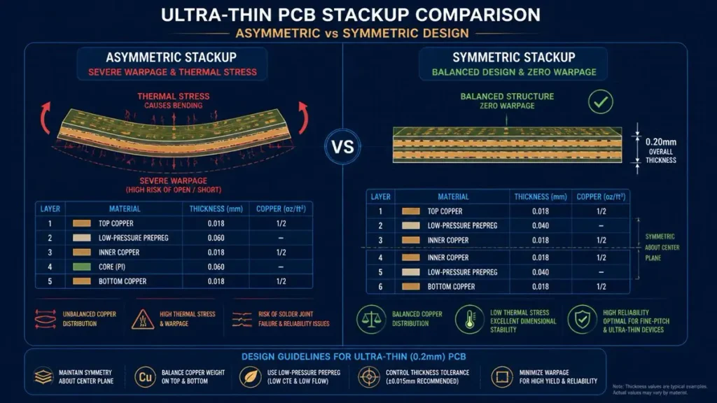
Ultra-Thin PCB Stackup Comparison: Symmetric vs Asymmetric Design for Warpage Control
Symmetric Stackup Architecture to Prevent Warpage
Warpage is the single largest yield killer in thin PCB design for high density interconnect. An asymmetric stackup—say, 1 oz copper on layer 1 and 0.5 oz on layer 2—creates a CTE mismatch that amplifies exponentially as total thickness decreases.
Thin PCB layout best practices for miniaturization mandate:
- Even layer counts (2, 4, 6) unless rigid-flex transition zones are engineered
- Mirror-image copper distribution around the center plane
- Identical prepreg resin content on both sides of the core
At PCBKR, our AI-driven stackup optimizer simulates CTE mismatch across the full reflow profile (25 °C → 260 °C → 25 °C) before CAM tooling. For a recent 0.25 mm, 6-layer AR headset project, this simulation predicted 0.38 mm bow and allowed us to adjust prepreg resin flow in pre-production—eliminating the rework cycle entirely.
Trace Routing and Spacing Rules for Ultra-Thin Boards
Ultra thin PCB design guidelines for trace geometry must account for both electrical performance and manufacturing fragility:
| Parameter | Conventional PCB | Ultra-Thin PCB (≤0.4 mm) | PCBKR 2026 Capability |
|---|---|---|---|
| Min trace/space | 3/3 mil (75/75 µm) | 2/2 mil (50/50 µm) | 1.5/1.5 mil (38/38 µm) mSAP |
| Min via diameter | 0.2 mm (mechanical) | 0.1 mm (laser) | 0.05 mm (UV/CO₂ hybrid) |
| Aspect ratio | 10:1 | 8:1 (fragile) | 12:1 with reinforced entry |
| Impedance tolerance | ±10% | ±5% required | ±2% with LDI |
Critical rule: Avoid 90° corners in thin PCB layout. Stress concentrates at the inner corner of a right-angle trace; on 0.2 mm material, this is where cracks initiate during V-scoring or depaneling. Use 45° or arc transitions instead.
Microvia and Via-in-Pad Strategies for Space-Constrained Designs
In HDI thin PCB design, every via steals space that could carry signal or power. Blind and buried vias are mandatory, but their placement requires DFM discipline:
- Place microvias ≥0.5 mm from board edges to prevent breakout during routing
- Use via-in-pad with copper fill (IPC-4761 Type VII) for BGA pitches below 0.4 mm
- Stagger stacked microvias rather than stacking them directly unless the supplier has proven sequential lamination with ±25 µm layer-to-layer registration
PCBKR operates Mitsubishi UV/CO₂ hybrid laser drills with automated optical registration. For a 0.3 mm, 8-layer medical telemetry board, we achieved 50 µm blind vias in 0.1 mm dielectric with zero misregistration across 1,200 panels—critical because the customer’s 0.35 mm BGA pitch left no room for annular ring compromise.
Ultra Thin PCB Material Selection Guide for RF and High-Reliability Applications
Substrate Options: When FR4 Ends and Advanced Materials Begin
Ultra thin PCB material selection is not simply about dielectric constant. For boards below 0.4 mm, the substrate must survive lamination, drilling, and multiple reflow cycles without delamination or CAF growth.
| Material | Thickness Range | Best For | Limitation |
|---|---|---|---|
| Standard FR4 (IT180A) | 0.1–0.8 mm | Cost-driven consumer | Df ~0.018; poor for >10 GHz |
| High-Tg FR4 (S1170) | 0.1–0.6 mm | Automotive under-hood | Higher cost, limited flexibility |
| Polyimide (PI) | 0.025–0.2 mm | Flex and rigid-flex | Moisture absorption; needs coverlay |
| Modified epoxy / LCP | 0.05–0.3 mm | 5G mmWave, 77 GHz radar | Limited supplier base |
| Glass substrate + low-CTE cloth | 0.1–0.4 mm | AI server, 224G PAM4 | Emerging 2026 tech; premium cost |
For ultra thin PCB design guidelines for medical devices, we typically specify adhesiveless polyimide with rolled-annealed copper. The elimination of acrylic adhesive reduces thickness by 20–30 µm per layer and eliminates the weakest link in dynamic flex cycling.Copper Foil and Surface Finish Decisions
On ultra-thin builds, copper foil contributes significantly to total thickness. Standard 1 oz (35 µm) copper plus plating adds ~50 µm per layer—unacceptable when the entire board must stay below 0.3 mm.
Ultra thin PCB cost optimization strategies should specify:
- 0.5 oz (17 µm) base copper for signal layers
- HVLP4-grade 3 µm ultra-thin carrier foil for high-speed layers (reduces skin effect loss)
- ENIG (Electroless Nickel Immersion Gold) for fine-pitch assembly; OSP is cheaper but risks coplanarity issues on 0.2 mm thin boards during reflow
PCBKR’s pulse-reverse electrolytic gold line delivers 15–80 µin hard gold with ±8% uniformity across 24-inch panels—critical for edge connector applications in 0.25 mm backplanes where contact reliability cannot degrade over 10,000 mating cycles.
How to Prevent Warpage in Ultra Thin PCB Design: A DFM Checklist
Pre-Layout Verification Steps
Before any Gerber leaves your desk, run this thin PCB DFM guidelines checklist:
- Stackup symmetry verification: Is the copper area on layer 1 within 5% of layer 2 (for 4-layer)? For 6-layer, match L1/L6, L2/L5, L3/L4.
- Component density balance: Are heavy BGAs or connectors placed asymmetrically? If so, add copper thieving (dummy copper) on the opposite side.
- Via density mapping: High via counts in one region create local stiffness. Distribute vias evenly or use filled microvias to equalize resin flow during lamination.
- Panelization strategy: For 0.2 mm boards, tab-routing with mouse bites outperforms V-scoring because it eliminates the stress concentration of a score line.
Manufacturing Process Controls That Procurement Should Audit
When visiting or qualifying an ultra thin PCB supplier, verify these process controls exist on the factory floor—not just in the brochure:
- Vacuum lamination with programmable pressure profiling: Standard hydraulic presses apply uniform pressure; thin cores require staged pressure release to prevent resin starvation.
- Real-time bow measurement post-etch: Inline laser profilometry should flag panels exceeding 0.3% bow before they reach electrical test.
- Low-stress depaneling: Router or laser depaneling for 0.2 mm boards; manual break-out is unacceptable.
- 100% 3D AOI + AXI for microvia quality: 2D AOI misses barrel cracks in 0.1 mm vias.
At PCBKR, our 2026 production line integrates Nordson DAGE 3D X-Ray for 100% microvia inspection, and our AI defect-classification system routes suspect panels to manual review before they reach shipping. This is why our first-pass yield on 0.25 mm, 6-layer HDI programs exceeds 99.7%.
Ultra Thin PCB Manufacturing Process Step by Step: What Buyers Must Know
From Core Preparation to Final Inspection
Understanding the ultra thin PCB manufacturing process step by step helps procurement teams ask the right questions during supplier audits:
Step 1: Material Cutting and Kissing
Thin cores are cut with diamond-coated blades at reduced feed rates to prevent edge fraying. At PCBKR, we use automated kissing (ultra-light contact) conveyors for cores below 0.1 mm to eliminate roller indentation.
Step 2: Laser Drilling and Desmear
UV/CO₂ hybrid lasers ablate dielectric without mechanical stress. For 0.2 mm boards, we use femtosecond pulses in polyimide layers to achieve 20 µm vias with <5 µm positional deviation—critical for any-layer HDI.
Step 3: Electroless Copper and mSAP Patterning
After desmear and activation, we deposit thin electroless copper, then use LDI to image 1.5 mil traces. The mSAP process adds copper only where needed, eliminating the etch undercut that plagues subtractive processing on thin cores.
Step 4: Sequential Lamination
Each lamination cycle must re-register to within ±25 µm. PCBKR’s automated optical alignment system uses four-point fiducial recognition with sub-pixel interpolation, achieving ±15 µm registration on 30-layer builds.
Step 5: Surface Finish and Electrical Test
Flying probe testing is preferred for prototypes; bed-of-nails fixtures risk mechanical damage to 0.2 mm boards. We use soft-tip probes with <50 g contact force.
Step 6: Final Metrology
Every ultra-thin panel is measured for thickness uniformity (±10% per IPC), bow/twist, and impedance coupon validation before release.
Thin PCB Supplier Selection Criteria 2026: A Procurement Scorecard
Technical Capability Thresholds
Not every supplier advertising “thin PCB capability” has invested in the equipment to deliver it. Use this scorecard when evaluating thin PCB supplier selection criteria 2026:
| Criterion | Minimum Acceptable | Best-in-Class (PCBKR Standard) |
|---|---|---|
| Min finished thickness | 0.4 mm | 0.1 mm rigid; 0.05 mm flex |
| Min trace/space | 3/3 mil | 1.5/1.5 mil mSAP |
| Min laser via | 0.1 mm | 0.05 mm |
| Layer-to-layer registration | ±50 µm | ±15 µm |
| Impedance control | ±10% | ±2% |
| Reflow simulation | None | AI-driven CTE mismatch prediction |
| Certifications | ISO 9001 | ISO 9001 + AS9100D + IATF 16949 + IPC-6012 Class 3 |
Supply Chain Resilience and DFM Engagement
The best ultra thin PCB supplier is not the one with the lowest quote—it is the one that prevents redesign. Ask these questions:
- Do they provide a complimentary DFM review with 24-hour turnaround?
- Can they share actual production data (yield rates, impedance distributions, thermal cycling results) from similar thin-board programs?
- Do they hold direct material agreements with Panasonic, Rogers, or Iteq for low-loss laminates, or will your 16-week lead time become 24 weeks because they buy through brokers?
At PCBKR, we maintain strategic inventory of Megtron 7/8, Tachyon 100G, and M9-grade hydrocarbon resin for customers running 224G PAM4 and 6G pre-research programs. Our engineering team reviews every stackup before tooling, and we guarantee a 30-minute quotation response for standard ultra-thin designs.
Application-Specific Ultra Thin Circuit Board Design Challenges and Solutions
Wearables and Consumer Electronics (0.2–0.4 mm)
How to design ultra thin PCB for wearables: Prioritize flex-to-rigid transitions with tear relief patterns. Use 0.5 oz copper on all layers, and specify ENIG to prevent fretting corrosion in connectors that experience daily flex.
Medical Implants and Diagnostic Patches (0.1–0.25 mm)
Ultra thin PCB design guidelines for medical devices require biocompatibility validation (ISO 10993) and hermetic sealing compatibility. Polyimide with rolled copper is standard; avoid nickel-bearing surface finishes if the device will contact tissue.
AR/VR Optics and 6G mmWave Modules (0.15–0.3 mm)
For 77 GHz automotive radar or 28 GHz 5G-Advanced modules, ultra thin PCB material selection guide for RF applications points to LCP or modified PTFE with Dk stability within ±0.02 across -40 °C to +85 °C. PCBKR’s M9 carbon-hydrogen + quartz cloth lamination achieves Dk 2.2–2.5 and Df ≤ 0.0005 at 10 GHz—critical for phase-array antennas where dielectric variation causes beam steering error.
Why Shenzhen Hongda Circuit Technology Co., Ltd. Is the Strategic Choice for Ultra-Thin PCB Programs
When your program demands ultra thin PCB design that transitions seamlessly from prototype to mass production, equipment lists matter. Here is what PCBKR brings to the procurement table:
- 3 µm HVLP4 ultra-thin carrier copper foil with vacuum sputtering + nano-electroplating, solving the peel-strength-versus-roughness trade-off
- LDI + mSAP hybrid imaging for 1.5 mil traces with ±2% impedance control
- Mitsubishi UV/CO₂/femtosecond laser drilling for 50 µm microvias in 0.1 mm dielectric
- Glass substrate lamination for AI server modules requiring CTE ≤ 14 ppm/°C and Tj control below 80 °C
- AI-driven warpage prediction integrated into CAM workflow, eliminating thermal-cycle surprises
- 104-layer backplane capability with sequential lamination and 3D X-Ray validation
- Zero-MOQ prototype policy with 48-hour quick-turn for qualified thin-board designs
We are not a broker. Every process step—from material cutting to final impedance testing—happens under one roof in Shenzhen, with full lot traceability and IPC-6012 Class 3 quality system oversight.
Frequently Asked Questions: Ultra-Thin PCB Procurement from a Buyer’s Perspective
What is the minimum practical thickness for a rigid ultra-thin PCB in high-volume production?
For rigid boards, 0.2 mm is the practical floor for most SMT assembly lines, though 0.1 mm is achievable with specialized carriers and laser depaneling. Below 0.2 mm, panel handling becomes the dominant cost driver. At PCBKR, we routinely produce 0.1 mm rigid-flex and 0.2 mm all-rigid panels at volume, using automated kissing conveyors and vacuum fixtures to prevent handling damage.
How do I verify that a supplier’s “ultra-thin capability” is real and not just marketing?
Request three things: (1) cross-section micrographs of a 0.2 mm or thinner production board showing via fill and copper uniformity; (2) impedance histograms from a recent high-volume lot to confirm process control; (3) a live video or audit of their thin-core lamination and depaneling stations. A supplier with genuine capability will provide these without hesitation. PCBKR shares all three during initial qualification, along with AS9100D and IATF 16949 audit reports.
Why does my ultra-thin PCB quote vary by 300% between suppliers?
The spread usually comes from three hidden variables: material grade (standard FR4 vs. high-Tg / low-loss), process technology (subtractive etch vs. mSAP), and inspection rigor (2D AOI vs. 3D AXI). A quote that seems too low often omits sequential lamination cycles or uses mechanical drilling that cannot achieve your via density. Always request a stackup-specific DFM review to expose these gaps before comparing prices.
What surface finish works best for ultra-thin boards with fine-pitch BGAs?
ENIG (Electroless Nickel Immersion Gold) is the default choice for pitches below 0.4 mm because it delivers flat, coplanar pads. On 0.2 mm boards, avoid HASL—the thermal shock and uneven surface can cause BGA voiding. For edge connectors or high-wear interfaces, specify hard gold (15–80 µin) over nickel. PCBKR’s pulse-reverse gold line maintains ±8% thickness uniformity even on 0.15 mm edge tabs.
How can I reduce lead time on ultra-thin PCB prototypes without sacrificing quality?
The fastest path is to engage the supplier’s engineering team before your layout is frozen. At PCBKR, our 24/7 DFM team can review your preliminary stackup and flag manufacturability issues—such as asymmetric copper distribution or via placements too close to flex bends—within hours, not days. This pre-CAM collaboration typically cuts one to two prototype iterations, saving 10–14 days on programs with aggressive launch schedules.
Procurement Excellence Starts with Design-for-Manufacturing Partnership
Ultra-thin PCB design is not merely a layout exercise; it is a supply-chain decision that determines whether your miniaturization program launches on time or enters a cycle of rework and yield loss. The procurement teams that win in 2026 are those that evaluate suppliers on total cost of ownership—technical depth, DFM engagement, quality system maturity, and material supply chain resilience—rather than per-panel price alone.
If you are ready to move from specification to production, Shenzhen Hongda Circuit Technology Co., Ltd. invites you to submit your Gerber files and stackup requirements for a complimentary DFM review. Our engineering team will analyze your thin PCB layout for warpage risk, impedance feasibility, and microvia manufacturability, and return a detailed quotation within 30 minutes.
Contact:
📧 Sales: sales@pcbkr.com
📧 Engineering: pcb@pcbkr.com
📞 Phone: +86 0755 23720053
🌐 Website: www.pcbkr.com
📍 Address: Room 1608-1610, Research Development Comprehensive Building, Baoyunda Logistics Center, Baoan, Shenzhen, China
About Author
David Chen https://www.linkedin.com/in/pcbcoming
David Chen boasts an extensive professional background in PCBA manufacturing, PCBA testing, and PCBA optimization, with specialized expertise in high-precision PCBA fault analysis and rigorous PCBA reliability testing. The author has worked with high-layer-count server PCB fabrication, ultra-low-loss backplane stackups, and thermo-mechanical reliability optimization for AI infrastructure projects involving 112G and 224G PAM4 architectures. Skilled in complex circuit design and cutting-edge advanced PCB manufacturing processes, he delivers solutions that elevate product durability and performance across industrial applications. His technical articles focusing on PCBA manufacturing workflows and testing methodologies are widely cited by industry peers, research institutions, and technical platforms, solidifying his reputation as a recognized technical authority in the global circuit board manufacturing sector.