LoRa PCB Manufacturing: What Should OEM Buyers Verify Before Ordering?
LoRa PCB manufacturing requires more than fabricating a circuit board from Gerber files. OEM buyers should verify RF layout constraints, antenna clearance, material selection, impedance requirements, assembly quality, and production testing. Shenzhen Hongda Circuit Technology Co., Ltd. supports PCB manufacturing and PCBA assembly with engineering review and manufacturing processes matched to the design requirements.
What Does LoRa PCB Manufacturing Include?
LoRa PCB manufacturing can include bare-board fabrication, component assembly, design-for-manufacturing (DFM) review, electrical inspection, and production support. The required scope depends on whether the buyer needs a prototype PCB, an assembled wireless module, or a production-ready electronic assembly.
LoRa is a low-power, long-range wireless technology used in applications such as smart metering, environmental monitoring, asset tracking, smart agriculture, and industrial sensing. A LoRa product may use a pre-designed radio module or a discrete RF transceiver. That choice affects PCB layout, antenna integration, assembly requirements, and validation.
A typical LoRa PCB manufacturing project involves the following requirements:
| Project element | Information to confirm | Why it matters |
|---|---|---|
| Bare PCB fabrication | Gerber or ODB++ files, stackup, copper weight, finished thickness | Establishes the fabrication requirements |
| RF layout | Approved radio layout, feed geometry, ground arrangement | Reduces avoidable changes to RF-sensitive features |
| Antenna integration | Antenna type, keepout area, ground-plane requirements | Prevents conflicts with copper, components, and the enclosure |
| Component assembly | BOM, placement files, package details, approved alternatives | Reduces sourcing and assembly errors |
| Electrical inspection | Netlist, continuity and isolation requirements | Detects specified electrical defects |
| RF validation | Test points, test limits, fixtures, and responsibilities | Separates PCB inspection from radio performance testing |
For OEM buyers, the first decision is whether the supplier will manufacture only the bare PCB or also provide component sourcing, SMT/THT assembly, inspection, and agreed testing. These are different scopes and should be clearly defined in the quotation.
Which PCB Materials and Stackups Are Suitable for LoRa Devices?
Standard FR-4 is often suitable for LoRa boards using conventional sub-GHz radio modules, but the correct material and stackup depend on antenna design, RF feed geometry, board dimensions, dielectric properties, environmental conditions, and the approved reference layout.
Not every LoRa PCB requires a specialized high-frequency laminate. At common operating bands such as 433 MHz, 868 MHz, and 915 MHz, many designs can use appropriately specified FR-4. However, a printed antenna or controlled-impedance RF feed still requires careful layout and manufacturing control.
Buyers should evaluate five factors.
- Dielectric properties: The effective dielectric constant affects transmission-line impedance and the electrical length of a PCB antenna.
- Copper geometry: Copper thickness and finished trace dimensions influence conductor loss and impedance.
- Finished board thickness: Changes to dielectric thickness can alter the impedance of microstrip or coplanar-waveguide structures.
- Environmental exposure: Outdoor meters, agricultural sensors, and industrial monitors may face humidity, temperature cycling, and condensation.
- Mechanical constraints: Batteries, connectors, displays, shields, mounting holes, and enclosure walls can restrict the available antenna region.
For example, an OEM may initially specify a 1.6 mm FR-4 board and later reduce the thickness to fit a compact enclosure. That change is not purely mechanical. It can affect the RF feed geometry, antenna tuning, ground-plane relationship, and component clearances.
The revised stackup should therefore be reviewed before the production files are released.
When a design requires tighter control of dielectric properties or lower signal loss, buyers can evaluate high-frequency PCB manufacturing as an alternative. The material should be selected according to the actual RF requirements, not simply because the product uses LoRa.
How Do 868 MHz and 915 MHz Requirements Affect LoRa PCB Manufacturing?
The intended operating band affects antenna dimensions, matching, RF layout, and product validation. The PCB manufacturer needs the target frequency band and approved RF design before fabrication begins.
The 868 MHz and 915 MHz bands are common in LoRa deployments, but permitted frequencies, channel plans, and transmit-power limits depend on the target market and applicable regulations. A board designed for one region should not automatically be assumed to perform correctly in another.
A practical engineering review should confirm:
- Target market and frequency plan: Identify the intended region and operating channels.
- Radio implementation: Confirm the transceiver or module model and its reference layout.
- Antenna type: Specify whether the design uses a PCB trace antenna, chip antenna, spring antenna, or external antenna connector.
- Ground-plane geometry: Check the required ground area and antenna keepout against the actual board outline.
- Matching network: Preserve the approved component footprints and RF routing unless the design owner authorizes a change.
- Enclosure and nearby components: Assess the effects of batteries, displays, shields, cables, and mounting hardware.
Consider a smart-water-meter design that passes bench testing with the PCB outside its enclosure but loses communication range after installation. The cause may not be a fabrication defect. The enclosure, battery, metal mounting structure, or altered ground-plane geometry may detune the antenna or change its radiation pattern.
The manufacturing lesson is to control the antenna region, board outline, stackup, and nearby mechanical features as a connected set of design requirements. Changes to one element should trigger an engineering review of the potential RF impact.
How Should RF Impedance and Antenna Clearance Be Controlled During Manufacturing?

RF Impedance and Antenna Clearance Control in LoRa PCB Manufacturing
RF impedance and antenna clearance should follow the approved layout, stackup, transmission-line geometry, and design specification. A nominal 50 Ω RF feed is common, but the manufacturer should confirm the specified target rather than assume that every LoRa circuit uses the same impedance requirement.
The trace width required for a 50 Ω transmission line depends on dielectric thickness, dielectric constant, copper thickness, conductor geometry, and whether the design uses microstrip or coplanar waveguide.
Copying a trace width from another LoRa board is therefore unreliable. Two boards using the same general FR-4 material category may have different impedance because their finished stackups and conductor geometries differ.
A manufacturing review should cover these controls:
| Control item | Potential manufacturing problem | Recommended action |
|---|---|---|
| RF trace width and spacing | Etching changes the final conductor geometry | Review fabrication compensation and specified impedance requirements |
| Dielectric thickness | Stackup variation changes impedance | Confirm the finished stackup and relevant tolerances |
| Copper thickness | Changes conductor geometry and RF loss | Specify the required finished copper condition |
| Ground continuity | Layout changes or discontinuities affect the RF return path | Review the ground structure and critical connections |
| Antenna keepout | Copper, components, or mechanical parts enter the antenna region | Clearly define the keepout in design data and drawings |
| Matching-network footprints | Incorrect pads or substitutions affect the approved RF circuit | Control footprints, BOM revisions, and component orientation |
| Board outline | Mechanical changes alter the antenna environment | Define outline tolerances and revision control |
The key distinction is between design intent and manufactured geometry. The designer establishes the impedance target and antenna arrangement. The fabricator reviews manufacturability and follows the agreed process requirements.
If impedance is critical, the purchase specification should define the target, tolerance, verification method, and whether an impedance coupon and report are required.
A manufacturer’s imaging resolution alone does not prove that a finished LoRa antenna will be correctly tuned. Antenna performance also depends on the electrical design, surrounding materials, enclosure, and validation conditions.
Which PCB Manufacturing Technologies Improve LoRa Board Consistency?
Precision imaging, controlled lamination, laser drilling where needed, automated optical inspection, and suitable electrical testing can improve manufacturing consistency. The correct process depends on the board’s feature sizes, layer count, routing density, and specified acceptance criteria.
Shenzhen Hongda Circuit Technology Co., Ltd. uses manufacturing equipment and process technologies for different PCB production requirements. Their relevance to a LoRa project depends on the actual design rather than the technology label alone.
| Equipment or process | Stated capability or role | Potential relevance to LoRa projects |
|---|---|---|
| SCREEN Ledia laser direct imaging (LDI) | 8 μm imaging resolution; ±10 μm alignment capability | Supports accurate circuit imaging and registration for suitable designs |
| Mitsubishi UV/CO₂ laser processing | 75 μm microvia capability with ±5 μm positioning accuracy | Relevant to compact HDI designs that use laser-drilled microvias |
| LAUFFER vacuum lamination press | Vacuum capability below 50 mbar | Supports multilayer lamination and helps control trapped-air risks |
| Modified semi-additive process (mSAP), where qualified | Process option for fine conductor geometries | Relevant to dense routing when conventional subtractive processing cannot meet the approved design rules |
| Automated optical inspection (AOI) | Inspection of visible circuit patterns | Helps identify detectable shorts, opens, and pattern defects |
| X-ray inspection | Inspection of hidden features and solder joints where applicable | Useful for assemblies with concealed connections, including BGAs |
| Four-wire Kelvin and flying-probe electrical testing | Electrical verification using methods appropriate to the test plan | Helps verify continuity and resistance-related requirements on suitable boards |
These capabilities need to be interpreted correctly. LDI optical resolution is not equivalent to the minimum guaranteed finished line width. A laser-drilling specification does not mean every design using that via diameter is automatically manufacturable. Actual results depend on the complete process window, material system, artwork, copper processing, inspection criteria, and acceptance requirements.
For a straightforward two-layer LoRa sensor board, the priority may be reliable copper geometry, hole quality, solder-mask registration, and electrical continuity—not microvias or ultra-fine routing.
For a compact LoRa gateway or a densely integrated industrial controller, high-density interconnect technology may provide a genuine layout advantage. HDI PCB manufacturing can be evaluated when component density, routing congestion, or board-size constraints justify finer interconnect structures.
Where the design requires laser-drilled microvias, the buyer should also review microvia PCB fabrication to assess the applicable via structure, layer connection, reliability requirements, and manufacturing design rules.
Neither HDI nor microvias are automatically necessary for a LoRa product. They should be selected when the board architecture requires them.
What Manufacturing Problems Commonly Delay LoRa PCB Projects?
Common preventable delays include incomplete RF documentation, antenna keepout conflicts, stackup changes, unclear impedance requirements, component substitutions, and undefined acceptance criteria. These issues are easier to resolve during quotation and DFM review than after the first production batch.
Pain point 1: The Gerber files do not communicate the complete RF design intent
A fabrication package may contain all the copper layers yet omit important context. Without the stackup, impedance requirement, antenna keepout, or controlled revision, the supplier may not know which features are functionally sensitive.
Engineering response: Provide the fabrication drawing, layer stackup, finished copper requirements, impedance notes where applicable, board outline, and antenna keepout. Identify critical dimensions and any features that require approval before modification.
Pain point 2: A last-minute board-outline change moves the antenna
An enclosure engineer may shorten the PCB or relocate a mounting hole to accommodate a battery. This can reduce the antenna ground area or move conductive material into the keepout region.
Engineering response: Treat the antenna area and mechanical envelope as controlled design features. Review RF implications before approving revised fabrication files.
Pain point 3: A 50 Ω requirement is supplied without a complete stackup
The manufacturer cannot reliably determine the intended transmission-line geometry from the impedance target alone. Dielectric thickness, material properties, copper geometry, and tolerances also matter.
Engineering response: Submit the target impedance, proposed routing geometry, finished stackup, applicable tolerances, and verification method. Confirm whether impedance coupons and reports are included in the order.
Pain point 4: The prototype passes, but assembled units perform differently
A board tested outside its enclosure may behave differently after final assembly. Antenna tuning can change when a battery, display, cable, shield, or mounting bracket is added. Assembly substitutions may also affect RF layout and grounding.
Engineering response: Validate the product in its intended configuration. Control the BOM and approved alternatives, and define which changes require RF revalidation.
Pain point 5: The quotation does not define the testing boundary
A quotation may include bare-board electrical testing but exclude RF measurements, firmware loading, wireless range tests, or regulatory evaluation. If the scope is unclear, buyers may assume that unpriced tests are included.
Engineering response: Request an itemized scope covering bare-board electrical tests, assembly inspection, functional testing, RF measurements, documentation, and any external certification work. Mark each item as included, optional, or customer-supplied.
These problems are especially important when an OEM moves from a small engineering prototype to a pilot batch. A design that works in a single hand-built unit still needs documented fabrication, assembly, and acceptance requirements to support repeatable production.
How Should OEMs Validate LoRa PCB Quality Before Mass Production?
OEMs should validate bare-board fabrication, PCBA quality, and radio performance as separate but coordinated stages. Passing an electrical continuity test does not prove that the antenna, radio link, or finished product meets its performance requirements.
Stage 1: Bare-board acceptance
- Verify board dimensions, layer count, thickness, copper specification, surface finish, and revision.
- Perform the specified netlist, continuity, and isolation tests.
- Inspect visible copper features and other required manufacturing characteristics.
- Review controlled-impedance results when required by the purchase specification.
Stage 2: PCBA acceptance
- Check component part numbers, polarity, orientation, and placement against the approved BOM and assembly files.
- Inspect solder joints using AOI and, where appropriate, X-ray.
- Confirm workmanship criteria, rework rules, and component-substitution controls.
- Perform agreed power-on and functional tests.
Stage 3: RF and system validation
- Verify the RF path against the product test plan.
- Measure antenna matching or return loss when required and when the fixture and reference plane are defined.
- Check transmit and receive performance using suitable calibrated equipment and documented test conditions.
- Test the assembled product in its intended enclosure and installation environment.
- Complete applicable regional regulatory evaluation through the responsible product team or qualified laboratory.
For example, an industrial sensor may work on a laboratory bench but perform poorly after installation inside a metal cabinet. A meaningful validation plan should reproduce the actual installation conditions rather than rely solely on open-board testing.
RF measurements also require repeatable test setups. A VNA measurement without a defined calibration plane, fixture, cable arrangement, or acceptance threshold may be difficult to compare between suppliers or production lots.
Similarly, RSSI and wireless range depend on the radio configuration, antenna, environment, and test procedure. They should not be treated as universal PCB acceptance values.
How Can OEM Buyers Prepare an Accurate LoRa PCB Manufacturing RFQ?
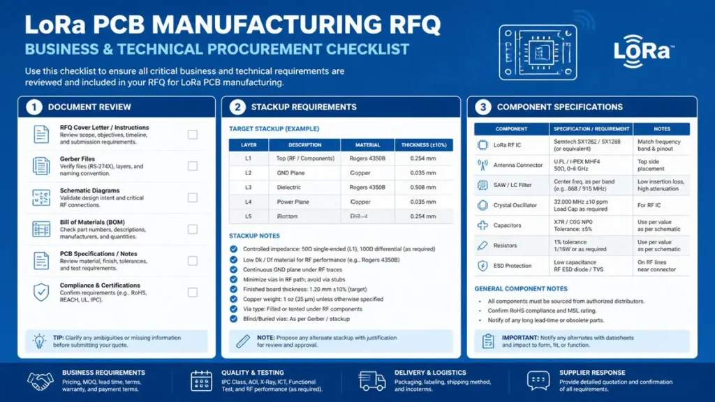
Business and Technical Procurement Checklist for LoRa PCB Manufacturing RFQ
Provide the current fabrication files, stackup, RF requirements, BOM and assembly data where applicable, target quantity, delivery requirements, and inspection scope. Complete information allows the manufacturer to quote the intended build instead of making assumptions that later create cost or schedule changes.
Use this checklist before requesting a quotation:
| RFQ input | Information to provide |
|---|---|
| Product and operating region | Application, target market, required frequency band |
| PCB fabrication files | Gerber or ODB++, drill files, board outline, fabrication drawing |
| Layer and material details | Layer count, material family, finished thickness, copper weight |
| RF design requirements | Approved layout, antenna type, keepout, feed geometry, impedance target where applicable |
| Mechanical constraints | Enclosure, mounting holes, connector locations, battery and shield clearances |
| PCBA files | BOM with manufacturer part numbers, centroid or placement file, assembly drawing |
| Quantity and schedule | Prototype quantity, pilot quantity, expected recurring volume, target delivery date |
| Quality requirements | Acceptance criteria, inspection requirements, electrical tests, traceability needs |
| RF/system test scope | Required measurements, test fixtures, pass/fail limits, responsible party |
| Change control | Revision identifier, approved alternatives, authorization required for substitutions |
If the RF design is still under development, state which items are provisional. An antenna matching network, for example, may require tuning after the first assembled prototype. That work should be identified as engineering validation rather than silently included in a bare-PCB quotation.
A useful quotation should identify assumptions, exclusions, material substitutions, tooling or test costs, and unresolved DFM issues. Buyers should compare suppliers against equivalent technical scopes, not unit price alone.
How Does Shenzhen Hongda Circuit Support LoRa PCB Manufacturing?
Shenzhen Hongda Circuit Technology Co., Ltd. supports custom PCB manufacturing and PCBA assembly, with engineering review and manufacturing processes selected according to the approved design and production requirements. For LoRa projects, the objective is to control fabrication and assembly variables while keeping RF performance validation tied to the agreed test plan.
Relevant manufacturing resources include precision laser direct imaging, vacuum lamination, laser drilling for applicable HDI structures, optical inspection, X-ray inspection for suitable assemblies, and electrical test methods.
These processes can address specific production risks, such as fine-feature consistency, multilayer registration, inspection of hidden solder joints, or electrical continuity. Their relevance should be assessed against the board design and the buyer’s acceptance criteria.
A technically sound supplier review should establish:
- Whether the proposed stackup and geometry are manufacturable.
- Whether impedance requirements are sufficiently specified to be quoted and verified.
- Whether the supplier can provide the required inspection records and electrical test results.
- Whether bare PCB fabrication and PCBA assembly scopes are clearly separated.
- Whether revisions, approved substitutions, and acceptance criteria are documented.
- Whether RF tuning and product certification are included, excluded, or managed by another party.
Not every LoRa board needs HDI, mSAP, ultra-fine traces, or specialized high-frequency laminate. These processes should be selected when the board size, routing density, electrical requirements, or reliability targets justify them.
A disciplined DFM review should establish the minimum process capability needed to manufacture the board consistently, identify unresolved design risks, and document the tests required before volume production.
For OEMs developing wireless sensors, smart meters, industrial monitoring equipment, and LoRa-enabled gateways, this approach helps create a clearer path from prototype fabrication to repeatable production.
What Should Buyers Ask a LoRa PCB Manufacturer Before Placing an Order?
Buyers should confirm the supplier’s manufacturing scope, RF controls, inspection methods, revision handling, and production readiness before issuing a purchase order. The following five questions help expose gaps before they become delivery or quality problems.
Can you manufacture the board to our specified stackup and impedance requirements?
Ask the supplier to review the actual stackup and RF geometry, identify missing specifications, and state whether impedance verification or test coupons are included. A generic claim of “50 Ω capability” is not a substitute for a project-specific review.
Can you supply both bare PCBs and assembled LoRa boards?
Confirm whether the quotation includes PCB fabrication only, component sourcing, SMT/THT assembly, inspection, and functional testing. Request separate line items where the scopes differ so competing quotations can be compared fairly.
What inspection and electrical test records will you provide?
Clarify whether the order includes AOI, X-ray where applicable, continuity and isolation testing, impedance reports where required, and inspection documentation. Agree on acceptance criteria before production starts.
How do you manage RF-sensitive design changes and component substitutions?
Ask whether a revised board outline, stackup, antenna region, matching-network footprint, or component alternative triggers engineering approval. Confirm how revisions are controlled and approved changes are recorded.
Can you support prototype, pilot, and repeat production using the same documented requirements?
Ask how the supplier preserves the approved BOM, fabrication revision, material specification, test limits, and inspection plan across repeat orders. If RF validation is required, clarify who performs it and how the results are documented.
A reliable quotation should answer these questions in writing. If a supplier cannot distinguish bare-board electrical testing from complete radio performance validation, clarify the scope before committing the order.
How Can You Request a LoRa PCB Manufacturing Quote?
Send the latest fabrication files, stackup, RF requirements, quantity, target schedule, and assembly scope so the supplier can review the requirements and identify missing information before quoting.
For a LoRa PCB prototype, PCBA build, or production quotation, contact Shenzhen Hongda Circuit Technology Co., Ltd.
- Email: pcb@pcbkr.com
- Website: https://www.pcbkr.com/
Include the board revision, target frequency band, antenna type, required testing, and any unresolved engineering constraints. If the project uses an antenna matching network that still requires tuning, identify that work separately from PCB fabrication and assembly.
A complete RFQ helps both parties establish a realistic manufacturing scope, clarify acceptance criteria, and reduce avoidable changes between prototype and production.
About Author
David Chen LinkedIn Profile
David Chen is a Senior RF/PCB Process Engineer at Shenzhen Hongda Circuit Technology Co., Ltd., with over 12 years of experience in high-frequency PCB fabrication, impedance-controlled stack-up design, and Rogers/PTFE laminate processing. He also boasts an extensive professional background in PCBA manufacturing, PCBA testing, and PCBA optimization, with specialized expertise in high-precision PCBA fault analysis and rigorous PCBA reliability testing. The author has worked with high-layer-count server PCB fabrication, ultra-low-loss backplane stackups, and thermo-mechanical reliability optimization for AI infrastructure projects involving 112G and 224G PAM4 architectures. Skilled in complex circuit design and cutting-edge advanced PCB manufacturing processes, he delivers solutions that elevate product durability and performance across industrial applications. His technical articles focusing on PCBA manufacturing workflows and testing methodologies are widely cited by industry peers and technical platforms, and have gained attention and recognition from industry colleagues.