HDI PCB DFM Guide for High-Volume Manufacturing
Minimum Trace Width, BGA Escape Routing, and mSAP vs. Subtractive Etching in 2026
Abstract
As printed circuit board assemblies push deeper into sub-50 µm conductor geometries, stacked microvias, and fine-pitch BGA territories in 2026, the gap between a board that can be designed and one that can be manufactured at scale is wider than ever. This guide, authored by the engineering team at Shenzhen Hongda Circuit Technology Co., Ltd., addresses the most critical design-for-manufacturability (DFM) decisions that separate successful high-volume HDI programs from costly respins: trace/space selection, microvia architecture, mSAP versus subtractive etching, via-in-pad discipline, and solder mask control. Whether you are designing a next-generation smartphone module, an automotive ADAS sensor board, or a high-density server backplane, the principles here translate directly to yield, cost, and delivery predictability.
Table of Contents
1. Why DFM Must Come Before Layout in HDI Programs
2. The Manufacturing Boundaries of HDI at Volume — 2026 Reference Data
3. Minimum Trace Width and Spacing: When to Use Subtractive Etching vs. mSAP
4. BGA Escape Routing: Fanout, Staggered Vias, and Via-in-Pad
5. Solder Mask Opening and Bridge Width Control
6. The Production-Ready DFM Checklist
7. High-Frequency Risk Points and Countermeasures in 2026 HDI
8. Emerging PCB Manufacturing Technologies Shaping HDI in 2026
9. Conclusion: Partnering DFM with Manufacturing Intelligence
Why DFM Must Come Before Layout in HDI Programs
HDI is not simply a routing problem. It is a manufacturing system problem that must be solved before the first copper trace is placed. In standard PCB design, the designer typically worries about signal integrity, impedance, and component placement — and hands off to manufacturing as a secondary concern. That model breaks down the moment a stackup crosses into HDI territory with buried vias, blind microvias, multiple lamination cycles, and sub-100 µm conductors.
At high volumes, the consequences of inadequate DFM compound quickly. A microvia aspect ratio that exceeds the plating window does not cause occasional failures — it drives systematic yield loss. Solder mask bridges that are marginally narrow in design become reliably broken on the production line when the mask layer drifts even slightly. BGA escape routing that works in simulation fails in volume when fine-pitch pads experience copper thickness variation across panel zones.
Shenzhen Hongda Circuit Technology Co., Ltd. processes tens of thousands of HDI panels per month. The most common cause of first-article failure is not signal integrity — it is geometry pushed beyond the stable process window. DFM must, therefore, be a design-phase activity, not a manufacturing-phase correction.
What DFM Governs in HDI
- Microvia structure: diameter, depth-to-diameter ratio, fill requirement, stacked vs. staggered
- Trace and space: inner layer vs. outer layer, conductor profile, etch uniformity
- Lamination count: each press cycle adds cost, alignment risk, and delamination exposure
- Registration tolerance: cumulative error across multiple laminations affects via-to-pad capture
- Solder mask: opening geometry, dam width, alignment capability of the coating process
Each of these variables has a stable production window. DFM means keeping the design inside that window — not at its edge.
The Manufacturing Boundaries of HDI at Volume — 2026 Reference Data
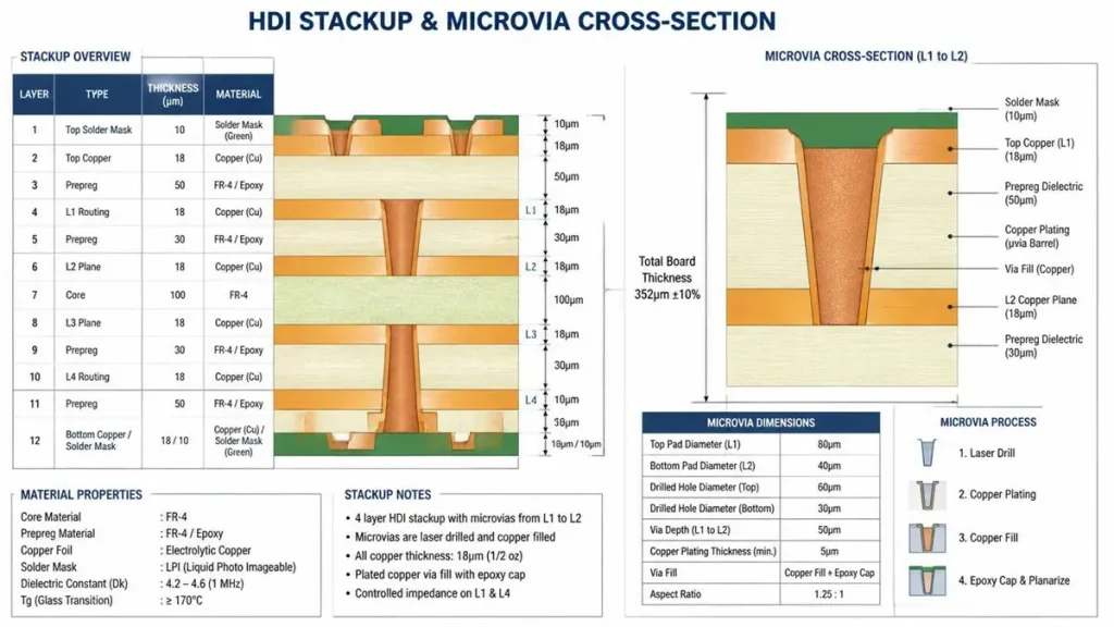
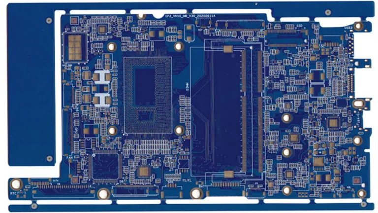
HDI Stackup and Microvia Cross-Section Diagram. This technical graphic illustrates a 4-layer HDI stackup utilizing laser-drilled, copper-filled blind microvias from L1 to L2, showcasing standard 2026 fabrication tolerances, dielectric thicknesses, and the step-by-step plating and planarization process required for high-volume manufacturing stability.
The following reference data reflects the stable production capabilities at HDI PCB Manufacturer Shenzhen Hongda Circuit Technology Co., Ltd. as of 2026. These values represent reliable, repeatable process windows at volume scale — not engineering limits achievable in prototype quantities only.
1. Trace Width and Space
Minimum trace and space for outer layers using conventional subtractive etching on standard HDI cores:
| Process Tier | Min. Trace Width | Min. Space | Typical Application |
| Standard HDI | 75 µm | 75 µm | Consumer electronics, IoT modules |
| Advanced HDI | 50 µm | 50 µm | Smartphones, wearables, RF boards |
| mSAP / SLP | 30–35 µm | 30–35 µm | High-end mobile, AI processors, HPC |
| Next-gen mSAP (2026) | 20–25 µm | 20–25 µm | Package substrates, advanced SiP |
Note: Inner-layer trace/space rules differ from outer layers. Always confirm with your manufacturer’s specific process capability document for both inner and outer layers.
2. Microvia Parameters
- Standard laser-drilled blind microvia: 80–100 µm diameter, ≤0.8:1 aspect ratio (depth:diameter)
- Advanced blind microvia (2026): 60–75 µm diameter with copper-filled electroplating and planarization
- Stacked microvias: maximum two-high stack in standard production; three-high requires design review and reliability qualification
- Staggered vias: preferred over stacked for most applications — lower manufacturing risk, better thermal reliability
- Via-in-pad (VIP): mandatory resin fill + electroplated cap; must be specified explicitly in fabrication notes
3. Lamination Cycles
Every additional lamination cycle in an HDI stackup adds process cost and compounds registration error. As a production planning rule:
- 1+N+1 HDI (one microvia layer each side): 2 lamination cycles — most manufacturable
- 2+N+2 HDI: 3 lamination cycles — manageable with tight process control
- 3+N+3 HDI: 4+ lamination cycles — higher cost, lower yield, reserved for advanced applications
Minimizing lamination cycles while meeting electrical requirements is one of the highest-value DFM decisions available to the designer.
Minimum Trace Width and Spacing: When to Use Subtractive Etching vs. mSAP
The choice between conventional subtractive etching and modified semi-additive process (mSAP) is arguably the most consequential process decision in an HDI design. It affects cost, lead time, yield, available supplier base, and the minimum achievable conductor geometry. In 2026, this decision is more nuanced than ever because both process families have advanced significantly.
1. Subtractive Etching — The Baseline Process
Subtractive etching starts with a fully copper-clad laminate and removes unwanted copper using photolithography and chemical etching. The etch factor — the ratio of vertical to lateral etch — determines how well narrow conductors can be resolved without undercutting. At 75 µm and above, subtractive etching is fully mature and cost-effective. At 50 µm, it remains viable with tight process control and thin starting copper foil (typically ½ oz or H/HOZ). Below 50 µm, lateral undercutting becomes a dominant failure mode that subtractive processes cannot reliably control at volume.
When Subtractive Etching Is Appropriate
- Target trace/space ≥ 75 µm: fully within stable subtractive window
- Target trace/space 50–75 µm: achievable with advanced subtractive, requires DFM review and tighter panelization
- Broad supplier availability: most qualified HDI manufacturers worldwide support subtractive at these geometries
- Lower tooling and NRE cost compared to mSAP
2. mSAP — When Fine Lines Become Non-Negotiable
Modified semi-additive process (mSAP) uses a thin copper seed layer on a dielectric, builds up conductors by selective copper plating, and then removes only a very thin seed layer — not a full copper foil. This approach virtually eliminates the undercutting problem and enables conductor widths and spaces down to 20–35 µm in 2026 production environments.
Shenzhen Hongda Circuit Technology Co., Ltd. operates qualified mSAP lines capable of 30 µm L/S in volume production as of 2026, with process development underway for 20 µm geometries for package substrate applications.
When mSAP Is the Right Choice
- Target trace/space ≤ 50 µm, especially for outer layers where subtractive control degrades
- High-layer-count SLP (substrate-like PCB) for advanced mobile processors
- Designs that demand consistent conductor cross-section for impedance uniformity
- Applications requiring extremely low loss tangent with ultra-fine routing (RF, mmWave)
- Next-generation AI inference modules and HPC interposers requiring 2026-tier density
Practical Decision Framework
| Target L/S | Recommended Process | Notes |
| ≥ 75 µm / 75 µm | Subtractive etching | Standard HDI; broadest supplier base |
| 50–75 µm / 50–75 µm | Advanced subtractive | Requires DFM review; thin foil specified |
| 35–50 µm / 35–50 µm | Advanced subtractive or mSAP | Borderline — confirm with fab |
| ≤ 35 µm / ≤ 35 µm | mSAP required | Evaluate supplier mSAP certification |
| ≤ 25 µm / ≤ 25 µm | Next-gen mSAP / SLP | Limited supplier base; long lead NRE |
BGA Escape Routing: Fanout, Staggered Vias, and Via-in-Pad
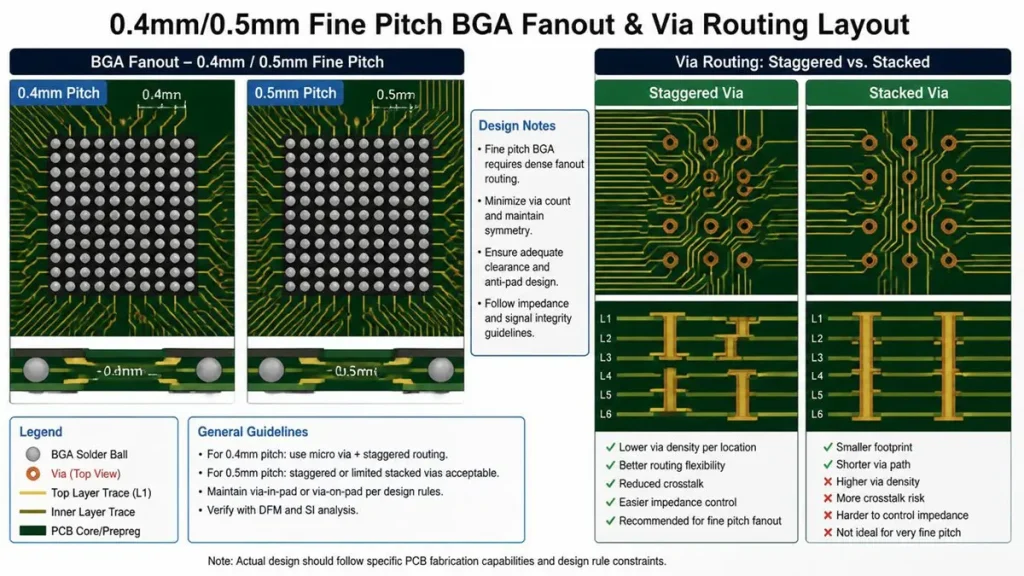
BGA Fanout and Via Routing Layout. Visualizing the tight geometry constraints of 0.4mm and 0.5mm fine-pitch BGAs alongside a structural cross-section comparison of staggered versus stacked microvia architectures for high-volume high-density programs.
Ball grid array escape routing is the point where HDI design constraints become most visible and most consequential. A BGA with 0.4 mm or 0.5 mm pitch cannot be fanned out using through-hole vias — the geometry simply does not fit. And as pitches continue to shrink in 2026 toward 0.35 mm and below for advanced packages, even standard blind microvias require careful placement discipline.
1. BGA Pitch and Escape Strategy by Tier
| BGA Pitch | Escape Strategy | Via Type | DFM Notes |
| ≥ 1.0 mm | Direct fanout with through-vias | Through-hole or blind | Straightforward; no HDI required |
| 0.8 mm | Mixed through-via and blind microvia | Blind microvias layer 1 | Standard HDI feasible |
| 0.65 mm | Blind microvia fanout | Staggered blind microvias | Confirm pad capture on L2 |
| 0.5 mm | Microvia fanout with via-in-pad | Via-in-pad with fill | Resin fill + electroplated cap required |
| 0.4 mm | Via-in-pad only; mSAP routing | Stacked or staggered VIP | Requires mSAP for escape traces |
| ≤ 0.35 mm | Full VIP + mSAP; SLP territory | Advanced VIP | Design review mandatory before release |
2. Via-in-Pad (VIP) Requirements
Via-in-pad places a blind or through microvia directly within the solder pad, eliminating the need for a breakout trace. This is essential for fine-pitch BGA but introduces additional manufacturing requirements that must be explicitly called out in fabrication notes.
- Resin fill: non-conductive epoxy fill eliminates the solder wicking path through the via
- Copper cap plating: electroplated copper over the filled via restores a flat, solderable surface
- Planarization: mechanical or chemical planarization ensures the cap sits flush with the surrounding pad — critical for solder paste printing consistency
- IPC-4761 specification: type VII (filled and capped) is the standard for production via-in-pad — specify this explicitly
A common DFM error is specifying via-in-pad in the schematic or layout without flagging fill and cap requirements in the fabrication drawing. The default assumption at many manufacturers is an unfilled via. Always state ‘IPC-4761 Type VII, resin fill with copper cap and planarization’ explicitly.
3. Staggered vs. Stacked Microvias for BGA Escape
Stacked microvias (one blind via placed directly on top of another across layers) offer a compact footprint but impose strict requirements on via filling quality. An insufficiently filled lower via creates a void that can collapse the upper via copper during lamination, leading to open circuits or intermittent connectivity.
Staggered microvias (each blind via offset horizontally from the via below) eliminate this concern entirely at the cost of a slightly larger routing footprint. For most high-volume programs, Shenzhen Hongda Circuit Technology Co., Ltd. recommends staggered microvias unless layer count or routing density makes stacking unavoidable — and when stacking is required, via fill quality must be confirmed with cross-section coupons.
Solder Mask Opening and Bridge Width Control
Solder mask is not just a protective coating. In dense HDI assemblies, it is an active participant in electrical isolation, particularly between fine-pitch BGA pads, QFN thermalpads, and high-density connectors. Solder mask DFM failures are among the most common causes of board-level yield loss in volume production — and among the most preventable.
1. The Failure Modes of Inadequate Solder Mask Control
- Solder mask bridge collapse: a dam that is too narrow will develop cracks or full breaks under thermal cycling, creating short-circuit risk between adjacent pads
- Misregistration: solder mask exposure on a fine-pitch BGA can shift during coating, exposing copper between pads (creating solder bridging risk) or covering pad edges (reducing solder joint area and strength)
- Solder ball wicking: an open via adjacent to a pad, without proper solder mask coverage, provides a wicking path that draws solder off the joint and into the via — particularly dangerous in via-in-pad designs that are not properly filled
2. Minimum Solder Mask Parameters — 2026 Production Reference
| Parameter | Standard Capability | Advanced Capability | Design Note |
| Min. SM opening (dia.) | 75 µm | 50 µm | Confirm with fab for sub-75 µm |
| Min. SM bridge (dam) | 75 µm | 50 µm | < 75 µm requires design review |
| Registration accuracy | ±25 µm | ±15 µm | Tighter = higher cost tier |
| Mask thickness | 15–25 µm over copper | 10–15 µm | Thin mask for fine feature SM |
| LDI (laser-direct imaging) | Standard | Required < 50 µm bridge | Specify LDI for fine pitch SM |
3. Critical DFM Rule: Solder Mask Designed to Fab Capability, Not CAD Defaults
PCB design tools typically apply default solder mask expansion and bridge values that may not match the actual capability of the manufacturer. A 50 µm solder mask bridge that looks clean in EDA software may be systematically undersized for the coating process. Before finalizing any fine-pitch solder mask design, obtain the specific solder mask process capability data from your manufacturer — not from a generic design rule check — and adjust expansion values accordingly.
The Production-Ready DFM Checklist
The following checklist is structured around the three phases where DFM decisions are made: before routing begins, during active layout, and after Gerber generation. Each item represents a confirmed failure mode observed in volume HDI production.
Phase 1: Pre-Layout (Stackup and Process Selection)
- Has the target trace/space been confirmed against the manufacturer’s specific process capability document (not a generic spec sheet)?
- Are inner-layer and outer-layer trace/space rules defined separately — they are not the same?
- Is the laminate material specified for the operating frequency, not just the layer count?
- Has the blind microvia diameter and aspect ratio been confirmed as within the plating process window?
- Has the lamination cycle count been minimized — can the same electrical result be achieved with fewer press cycles?
- Has mSAP vs. subtractive etching been evaluated based on the actual minimum conductor requirement?
- Has the impedance stackup been designed with the manufacturer, not calculated from generic stack models?
Phase 2: Active Layout (Routing and Via Architecture)
- Does every BGA escape routing fanout match the BGA pitch tier in Section 4.1 of this guide?
- Are all via-in-pad locations flagged for resin fill and electroplated copper cap (IPC-4761 Type VII)?
- Have stacked microvias been reviewed for fill quality requirement — and staggered alternatives considered?
- Are differential pair routing rules maintained across layer transitions with matched via-pair geometry?
- Has the return current path been verified for every layer transition via?
- Is via count minimized — redundant vias on power planes add lamination stress and add cost?
- Are test access points defined that do not conflict with component keepouts and solder mask dams?
Phase 3: Post-Gerber (Verification and Release)
- Has solder mask bridge width been verified against actual fab capability data — not CAD rule check defaults?
- Has solder mask registration tolerance been confirmed for all fine-pitch BGAs and QFNs?
- Are test coupons specified for trace width, space, and microvia cross-section verification?
- Is via fill and planarization specified explicitly in fabrication notes for all VIP locations?
- Has a pre-DFM review been submitted to the manufacturer before Gerber release?
- Is the final process selection (subtractive or mSAP) confirmed and documented in the fabrication specification?
High-Frequency Risk Points and Countermeasures in 2026 HDI
The following six failure categories account for the majority of HDI program respins and production yield loss events observed at Shenzhen Hongda Circuit Technology Co., Ltd. across 2024–2026 production data.
Risk 1: Trace and Space Beyond the Stable Etch Window
Designing 50 µm traces using a process line calibrated for 75 µm is not an engineering stretch — it is a systematic yield driver. The countermeasure is process selection discipline: match the minimum required conductor geometry to the correct process tier before design begins, not after.
Risk 2: Excessive Blind and Buried Vias Driving Lamination Count
Every blind/buried via layer requires a dedicated lamination cycle. Designs that add microvia layers without evaluating the lamination count impact frequently arrive at 4+ press cycles without realizing it. Countermeasure: conduct a lamination count audit at the stackup stage; collapse layers wherever the electrical penalty is acceptable.
Risk 3: Stacked Microvia Reliability Failures
Stacked microvias under thermal cycling are a well-documented reliability risk in HDI, particularly in automotive and industrial applications subject to wide temperature excursions. The IPC-6012 Class 3 requirements for via structures reflect this. Countermeasure: use staggered microvias by default; qualify stacked structures with cross-section and thermal cycling data before committing to a design.
Risk 4: Solder Mask Bridge Failure at Fine Pitch
A solder mask dam that is 10 µm narrower than the stable process window will fail — not occasionally, but systematically under thermal stress. Countermeasure: design to confirmed fab capability data, specify LDI exposure for sub-75 µm dams, and include solder mask coupon measurements in the first-article inspection plan.
Risk 5: BGA Escape Routing Incompatible with Pitch
Fine-pitch BGA designs routed without via-in-pad when VIP is required will fail DRC at the manufacturer and require rerouting. In 2026, 0.4 mm and 0.35 mm BGA packages are increasingly common in edge AI and automotive ADAS applications. Countermeasure: define BGA escape strategy at schematic stage based on the pitch table in Section 4 before placing a single route.
Risk 6: Missing Test Coupons for Volume Qualification
Releasing an HDI design to volume production without specifying test coupons for trace/space verification, microvia cross-section, and impedance validation removes the only independent check on whether the process delivered what the design required. Countermeasure: specify IPC-2221 coupons for conductor width/space and dedicated cross-section coupons for microvia qualification on every production panel.
Emerging PCB Manufacturing Technologies Shaping HDI in 2026
The HDI PCB landscape in 2026 is not standing still. Several process and material developments are reshaping what is manufacturable, what is reliable, and what is economically viable at high volume.
1. Any-Layer HDI and Every-Layer Interconnect (ELIC)
Any-layer HDI — where every layer in the stackup can be interconnected by a blind microvia — has moved from advanced prototype to volume production for premium smartphone applications. ELIC (Every Layer Interconnection) extends this to full-layer-pair freedom, enabling routing densities previously achievable only on package substrates. In 2026, Shenzhen Hongda Circuit Technology Co., Ltd. supports any-layer HDI with confirmed fill-stack technology for select customer programs.
2.Substrate-Like PCB (SLP) at Scale
SLP technology, which applies semiconductor packaging process discipline to PCB manufacturing, has expanded beyond the flagship smartphone segment into high-performance computing modules, automotive ADAS domain controllers, and advanced medical imaging electronics in 2026. The defining characteristics — mSAP conductor formation, sub-35 µm L/S, ultra-low-profile dielectrics — are now being qualified by a broader tier-one manufacturing base.
3. Laser-Drilled Microvia Size Reduction
CO2 and UV laser drilling systems deployed in 2025–2026 are achieving consistent 50 µm and below microvia diameters in production, down from the 80–100 µm that was standard just three years ago. Smaller microvias enable tighter via-to-trace spacing in BGA escape zones and reduce the land area required for via capture pads, contributing directly to routing density improvement.
4. Low-Loss and Ultra-Low-Loss Dielectrics
The expansion of 5G mmWave, automotive radar (77 GHz), and satellite communication electronics has driven rapid adoption of low-loss (Df < 0.005) and ultra-low-loss (Df < 0.002) laminate materials in HDI stackups. These materials impose stricter DFM requirements — surface finish compatibility, bonding film selection, drill parameter adjustment — and must be designed for with material-specific DFM rules, not generic FR4 assumptions.
5. Additive and Semi-Additive Process Expansion
Beyond mSAP, fully additive copper deposition processes are progressing toward production qualification for PCB applications in 2026. These processes deposit conductor material only where needed, eliminating etch waste and enabling sub-15 µm conductors on certain substrate types. While not yet mainstream for PCB production volumes, the technology trajectory suggests it will be commercially significant within the next design cycle for package substrate and advanced interposer applications.
6. Advanced Surface Finishes for Fine-Pitch Assembly
ENEPIG (Electroless Nickel Electroless Palladium Immersion Gold) has largely displaced ENIG in fine-pitch HDI applications as of 2026, owing to its superior wire bonding compatibility, resistance to black pad phenomenon, and consistency on very small pad geometries. For sub-0.4 mm BGA assemblies, ENEPIG should be the default finish specification unless cost constraints drive a deliberate tradeoff decision.
Partnering DFM with Manufacturing Intelligence
HDI PCB design-for-manufacturability in 2026 is not a checklist exercise performed at the end of layout. It is a continuous engineering discipline that begins at stackup selection, runs through every routing decision, and culminates in a fabrication specification that communicates process requirements unambiguously to the manufacturer.
The core principles are consistent regardless of how the process landscape evolves: keep conductor geometries inside the stable process window for your chosen manufacturing tier; design microvia architecture for the fill and registration capability of the process, not for theoretical compactness; define BGA escape strategy based on BGA pitch before routing begins; and never assume solder mask parameters from CAD defaults.
Shenzhen Hongda Circuit Technology Co., Ltd. provides pre-DFM review services as a standard part of the engineering engagement for new HDI programs. Our process engineers review Gerbers and stackup files against our current production capability data — not against generic IPC tables — and return specific, actionable feedback before any tooling is cut.
The objective is not to find problems after they become yield losses. The objective is to design them out before the panel ever reaches a press.
About Shenzhen Hongda Circuit Technology Co., Ltd.
Shenzhen Hongda Circuit Technology Co., Ltd. is a professional PCB manufacturer based in Shenzhen, China, specializing in high-density interconnect (HDI) boards, flexible and rigid-flex circuits, and advanced multilayer PCBs for consumer electronics, automotive, industrial, and telecommunications applications. With certified processes across IPC-6012 Class 2 and Class 3 requirements and active mSAP line qualification, Hongda serves global customers requiring volume-scale manufacturing of technically demanding PCB assemblies.
For DFM review requests, technical questions, or manufacturing capability inquiries, contact the Hongda engineering team through the company website.
FAQ
What is a safe minimum trace width and spacing to use when mass-producing HDI PCBs?
This depends on the factory’s process capability, layer count, materials, and yield rate targets. For conventional HDI mass production projects, it is highly recommended to design within the factory’s mature process window rather than pushing for extreme limits. If your design is already approaching ultra-fine trace widths and spacing, you need to evaluate early on whether to switch to a manufacturing route better suited for fine-line geometry.
Why are solder mask openings and solder mask dams so critical for HDI mass production?
In high-density layouts, the solder mask affects not only soldering reliability but also short-circuit risks and assembly yields. Especially in BGA and fine-pitch device areas, solder mask dams that are too narrow or significant alignment deviations will drastically increase manufacturing risks.
What key parameters should procurement verify with the factory when quoting HDI PCBs?
At a minimum, you should confirm the minimum trace width/spacing, microvia diameter, number of lamination cycles, support for blind/buried vias, capability for via-in-pad filling, plating flatness (coplanarity), as well as solder mask registration and testing capabilities. Confirming these parameters upfront can significantly reduce prototyping rework and mass production risks.
About Author
David Chen https://www.linkedin.com/in/pcbcoming
David Chen boasts an extensive professional background in PCBA manufacturing, PCBA testing, and PCBA optimization, with specialized expertise in high-precision PCBA fault analysis and rigorous PCBA reliability testing. The author has worked with high-layer-count server PCB fabrication, ultra-low-loss backplane stackups, and thermo-mechanical reliability optimization for AI infrastructure projects involving 112G and 224G PAM4 architectures. Skilled in complex circuit design and cutting-edge advanced PCB manufacturing processes, he delivers solutions that elevate product durability and performance across industrial applications. His technical articles focusing on PCBA manufacturing workflows and testing methodologies are widely cited by industry peers, research institutions, and technical platforms, solidifying his reputation as a recognized technical authority in the global circuit board manufacturing sector.