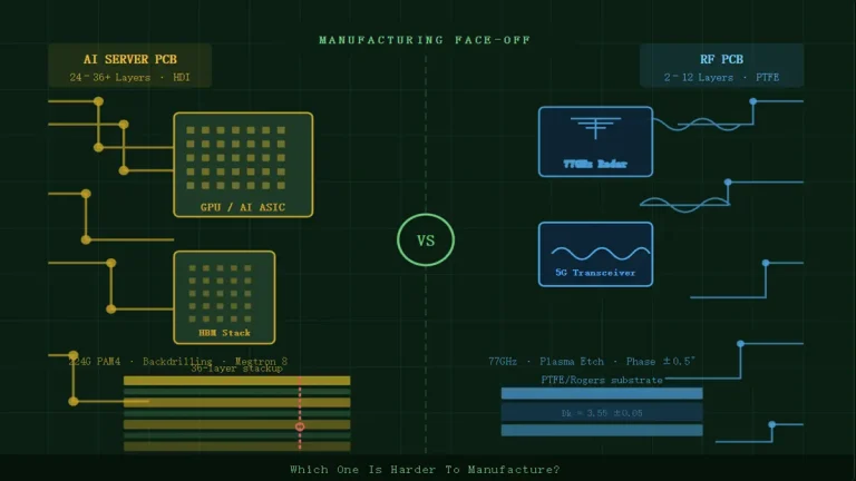
How CTE Mismatch Causes Delamination in AI Backplanes
AI Backplanes operate under extreme thermal cycling, high current density, and ultra-low-loss material requirements. In modern AI Backplanes, CTE mismatch between copper, resin systems, glass fabric, and large BGA packages is one of the leading root causes of delamination, barrel cracking, CAF risk, and long-term reliability failure.
What Is CTE Mismatch in AI Backplanes?
The Root Mechanism
Delamination in AI Backplanes occurs because repeated thermal expansion differences generate interfacial shear stress that eventually exceeds the adhesion strength between laminate layers, resin systems, and copper interfaces. In 112G and 224G PAM4 architectures, the problem becomes substantially worse because ultra-low-loss channel requirements force manufacturers to adopt smoother copper foils and hybrid low-loss dielectric systems.
Why 224G PAM4 AI Backplanes Exacerbate Delamination Risks
The Low-Loss Copper Reliability Tradeoff
Modern 224G PAM4 AI Backplanes require extremely low insertion loss at Nyquist frequencies approaching 56 GHz. To achieve this, manufacturers increasingly use HVLP1, HVLP2, and ultra-low-profile copper foils with extremely smooth copper surfaces.
However, smoother copper directly reduces the mechanical bonding strength between copper and resin systems. Traditional rough copper surfaces create stronger resin anchoring through mechanical tooth-like interlocking. Ultra-smooth copper weakens this peel strength, making the copper-resin interface far more vulnerable during thermal cycling.
In practical AI Backplane manufacturing, this creates a dangerous reliability chain:
- Higher PAM4 speeds require lower conductor loss
- Lower conductor loss requires smoother copper foil
- Smoother copper reduces resin adhesion strength
- Weaker interfaces amplify CTE mismatch stress
- Thermal cycling accelerates interfacial separation
This is one of the most overlooked reliability tradeoffs in next-generation AI Backplanes.
Failure Mechanism Inside AI Backplanes
During operation, AI Backplanes repeatedly cycle between ambient temperatures, assembly reflow temperatures, GPU hotspot regions, and high-current power delivery hotspots.
- Copper expands slowly
- Resin systems expand faster
- Pure PTFE (unfilled) expands dramatically in the Z-axis
- Ceramic packages barely expand
Over thousands of cycles, stress accumulates at weak interfaces including resin-to-copper boundaries, prepreg interfaces, via corner regions, and large BGA escape routing areas.
What Are the Most Common Delamination Locations in AI Backplanes?
| Risk Area | Failure Type | Typical Trigger |
|---|---|---|
| Large BGA corners | Interfacial cracking | Package warpage |
| Backdrilled vias | Resin separation | Thermal stress concentration |
| Pure PTFE/FR-4 transition zones | Layer separation | Extreme CTE mismatch |
| Thick copper PDN areas | Resin fatigue | Local rigidity increase |
Real Manufacturing Observation
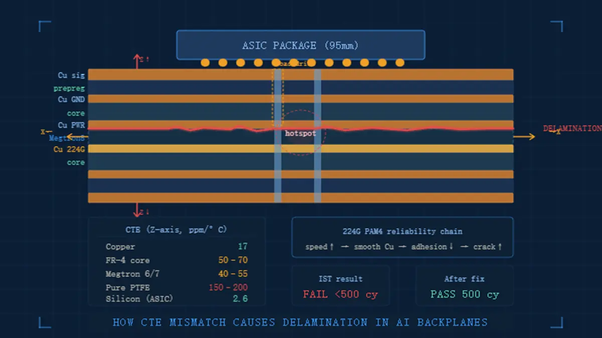
Our engineering team at PCBKR recently resolved a delamination issue in a 38-layer AI Backplane developed for an 800G GPU training cluster. Repeated IST testing revealed early-stage delamination around the backdrilled via fields beneath 95 mm ASIC packages after extended thermal cycling.
Cross-section analysis showed resin recession, localized copper separation, and weakened bonding interfaces around HVLP copper regions used for 224G PAM4 signal routing.
The root causes included:
- Mixed dielectric stackups with different curing windows
- Excessive local copper density imbalance
- Insufficient resin flow during multilayer lamination
- Z-axis CTE mismatch exceeding 55 ppm/°C in localized regions
- Reduced peel strength caused by ultra-smooth low-profile copper foil
After redesigning copper balancing structures, optimizing lamination pressure profiles, and migrating to a ceramic-filled hydrocarbon resin system with lower Z-axis expansion, the final stackup successfully passed 6× lead-free reflow cycles followed by 500 cycles of IST testing with a resistance change of less than 10%, representing approximately a 2.7× improvement in thermal endurance compared with the original design.
How Do Hybrid Stackups Increase Delamination Risk?
| Material System | Electrical Advantage | Typical Cure Window | Mechanical Compatibility Risk |
|---|---|---|---|
| Standard FR-4 | Low manufacturing cost | 170-185°C | Higher dielectric loss at 112G/224G |
| Megtron 6 / Megtron 7 | Very low insertion loss | 190-210°C | Moderate Z-axis expansion mismatch |
| Megtron 8-class materials | Ultra-low-loss for 224G PAM4 | 210-230°C | Higher process sensitivity during lamination |
| Pure PTFE (Unfilled) | Exceptional RF performance | 300°C+ sintering behavior | High expansion mismatch and difficult multilayer compatibility |
| Ceramic-filled Hydrocarbon / PTFE systems | Low loss with improved thermal stability | 200-230°C equivalent lamination behavior | Preferred balance for advanced 224G AI Backplanes |
| PPO/PPE resin systems | Balanced SI and thermal reliability | 200-220°C | Pressure-window optimization required |
In AI Backplanes, hybrid stackups often combine multiple low-loss dielectric systems in the same multilayer structure. The problem is not only CTE mismatch — it is also cure-window incompatibility.
If two resin systems cure at different temperatures or shrink differently during lamination cooldown, residual internal stress becomes trapped inside the PCB structure. Under repeated GPU thermal cycling, those stresses accumulate near dielectric transition zones and eventually trigger interfacial delamination.
How Can AI Backplane Manufacturers Reduce Delamination Risk?
1. Use Low-Z-Axis-CTE Materials
- Panasonic Megtron 6
- Tachyon 100G
- Isola I-Speed
- Low-expansion hydrocarbon ceramics
2. Improve Resin Flow During Lamination
- Vacuum-assisted lamination
- Multi-stage pressure profiles
- Real-time press temperature monitoring
- Resin-flow simulation software
3. Optimize Copper Balancing
- Symmetrical copper density
- Balanced plane structures
- Reduced isolated copper islands
- Controlled thick-copper transitions
What Reliability Tests Detect Delamination in AI Backplanes?
| Test Method | Purpose | Typical Standard |
|---|---|---|
| IST Testing | Via fatigue & delamination | IPC-TM-650 |
| T260/T288 | Thermal resistance | IPC standards |
| Thermal shock cycling | Expansion fatigue | -40°C to 125°C |
| SAM scanning | Internal void detection | Acoustic microscopy |
Golden Summary: Why CTE Mismatch Is a Critical AI Backplane Reliability Problem
CTE mismatch is one of the most underestimated reliability threats in AI Backplanes because it silently accumulates mechanical stress during every thermal cycle.
The problem becomes dramatically worse in 224G PAM4 backplanes, hybrid dielectric stackups, ultra-thick multilayer structures, and high-current AI clusters.
The most reliable AI Backplanes are designed using a co-optimization strategy balancing signal integrity, thermal management, mechanical stability, lamination process control, and long-term material compatibility.
Frequently Asked Questions About AI Backplane Delamination
Can low-loss materials increase delamination risk in AI Backplanes?
Yes. Many ultra-low-loss materials have different mechanical expansion properties compared with FR-4. Without proper stackup engineering, they can increase internal stress and interfacial separation risk.
Why are large GPU packages dangerous for AI Backplanes?
Large ASIC packages create severe strain concentration near BGA corners because silicon, substrate materials, and PCB laminates expand at dramatically different rates.
Is PTFE risky in AI Backplanes?
Pure, unfilled polytetrafluoroethylene (PTFE) can introduce significant Z-axis thermal expansion mismatch and lamination challenges in multilayer AI Backplane structures. However, modern 224G AI Backplanes do not rely on pure PTFE alone. Instead, advanced ceramic-filled hydrocarbon/PTFE composite systems are used to maintain excellent dielectric performance while significantly stabilizing dimensional expansion and improving interlayer reliability under thermal cycling.
Need Expert Stackup Optimization for 112G/224G AI Backplanes?
PCBKR engineering specialists support AI infrastructure projects involving ultra-low-loss materials, hybrid stackups, backdrilling optimization, thermo-mechanical reliability analysis, and high-layer-count manufacturing.
Request a free DFM and reliability review: PCB@pcbkr.com
Using top-tier AI server PCB equipment to manufacture traditional PCBs delivers a strategic advantage: interlayer alignment tolerance shrinks from ±75μm to within ±25μm, and differential impedance control tightens to ±5%. Paired with 100% 3D X-Ray inspection, it grants conventional boards chip-level precision, superb signal stability, and near-100% yield.
Still, need help? Contact Us: sales@pcbkr.com
About Author
David Chen https://www.linkedin.com/in/pcbcoming
David Chen boasts an extensive professional background in PCBA manufacturing, PCBA testing, and PCBA optimization, with specialized expertise in high-precision PCBA fault analysis and rigorous PCBA reliability testing. The author has worked with high-layer-count server PCB fabrication, ultra-low-loss backplane stackups, and thermo-mechanical reliability optimization for AI infrastructure projects involving 112G and 224G PAM4 architectures. Skilled in complex circuit design and cutting-edge advanced PCB manufacturing processes, he delivers solutions that elevate product durability and performance across industrial applications. His technical articles focusing on PCBA manufacturing workflows and testing methodologies are widely cited by industry peers, research institutions, and technical platforms, solidifying his reputation as a recognized technical authority in the global circuit board manufacturing sector.