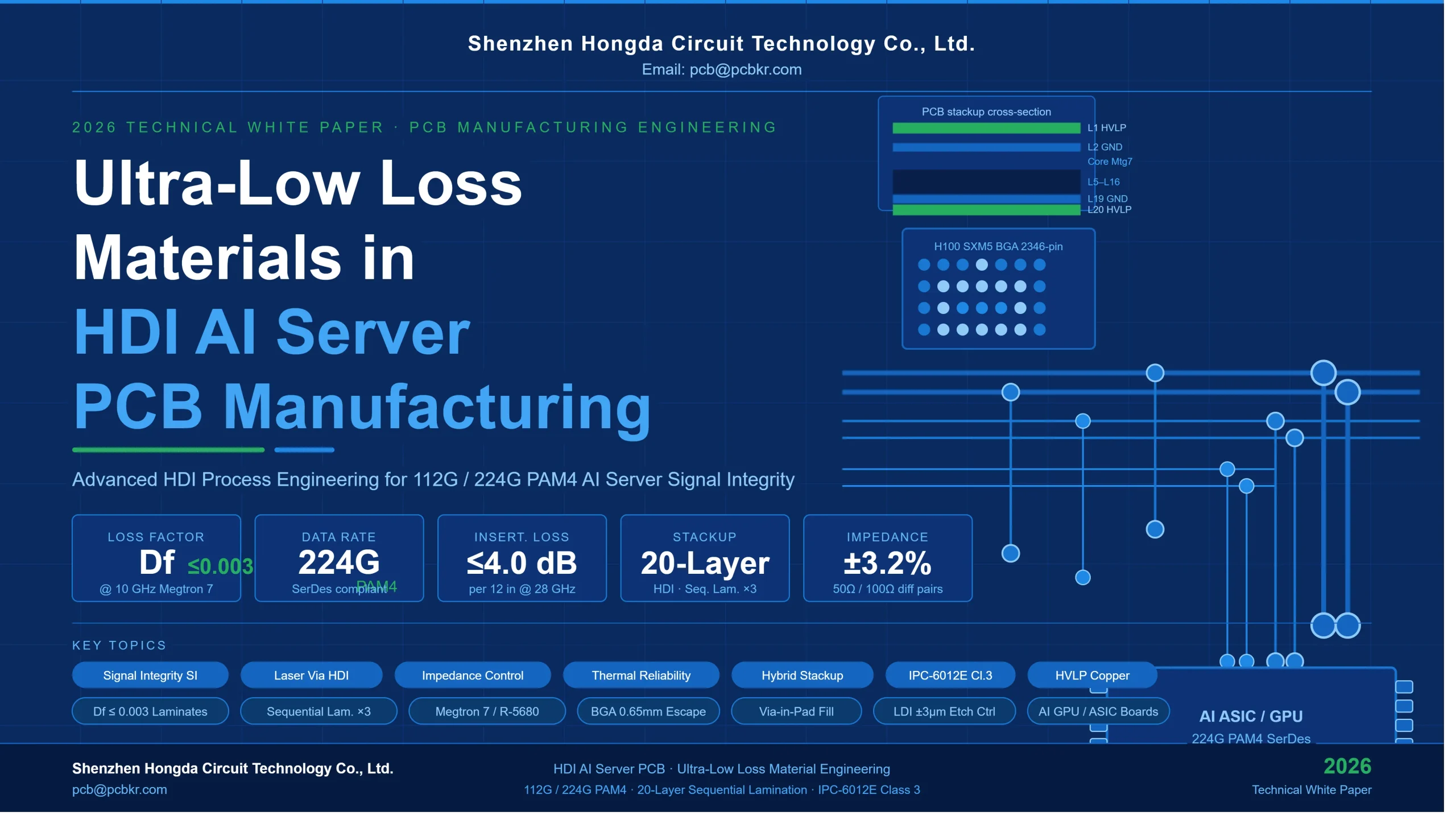
Ultra-Low Loss Materials in HDI AI Server PCB Manufacturing
Shenzhen Hongda Circuit Technology Co., Ltd. | 2026 Technical White Paper
Advanced PCB Engineering | AI Infrastructure | High-Speed Signal Integrity
Ultra-low loss PCB materials with Df < 0.003 are now essential for AI server HDI boards operating at 112G/224G PAM4 speeds. Shenzhen Hongda Circuit Technology Co., Ltd. achieves ≤0.8 dB/inch insertion loss at 28 GHz using modified PPO/PPE laminates in 20-layer HDI stackups, enabling GPU cluster interconnects with <1% BER at sustained 400G throughput.
What PCB Materials Enable 224G PAM4 Signal Integrity in AI Server Boards?
Only ultra-low loss laminates with Dk ≤ 3.5 and Df ≤ 0.003 at 10 GHz can support 224G PAM4 channels with eye diagrams that pass IEEE 802.3df mask requirements. At Shenzhen Hongda, our material qualification runs confirm that standard FR-4 (Df = 0.020–0.025) fails at channel lengths exceeding 8 inches for 112G NRZ, while our qualified PPO-based materials sustain compliance up to 22 inches.
Engineering Reality — The Signal Loss Budget:
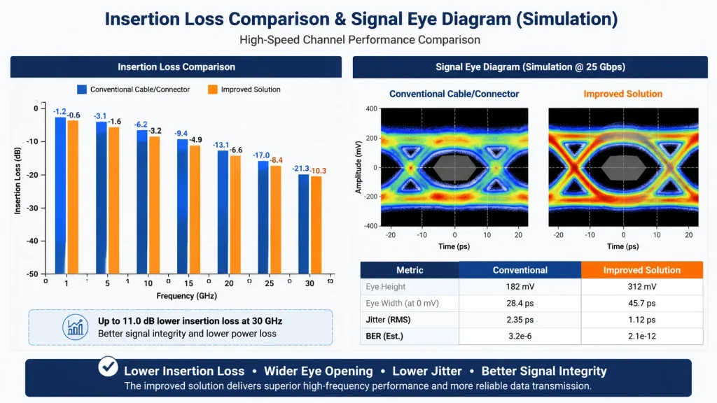
High-Speed Channel Insertion Loss and Signal Eye Diagram Simulation Comparison
In a typical AI GPU carrier board with 18-layer HDI construction, the total channel insertion loss budget for a 112G PAM4 SerDes link is governed by:
| Loss Component | FR-4 Standard | Low-Loss (Df 0.009) | Ultra-Low Loss (Df 0.003) | Hongda Spec 2026 |
| Dielectric loss @ 28 GHz / 10 inches | −6.4 dB | −2.9 dB | −1.1 dB | ≤ −0.9 dB |
| Conductor loss (1 oz Cu, 4 mil trace) | −3.1 dB | −3.0 dB | −2.9 dB | ≤ −2.8 dB |
| Via + pad transition loss (×4 vias) | −1.2 dB | −1.1 dB | −1.0 dB | ≤ −0.9 dB |
| Connector / package | −1.5 dB | −1.5 dB | −1.5 dB | ≤ −1.4 dB |
| Total channel loss | −12.2 dB | −8.5 dB | −6.5 dB | ≤ −6.0 dB |
| IEEE 802.3df 112G PAM4 limit | −7.0 dB ✗ FAIL | −7.0 dB ✗ FAIL | −7.0 dB ✓ PASS | −7.0 dB ✓ PASS |
Manufacturing Pain Point — Dk Tolerance Drift During Lamination:
One of the most underreported challenges in high-frequency PCB production is Dk variation across a panel. In our process engineering experience at Hongda, standard lamination cycles produce ±0.15 Dk variation across a 24″×18″ panel for PPO-based materials, which translates directly to ±3.2% impedance deviation on 50Ω differential pairs. Our 2026 protocol mandates:
- Lamination temperature ramp rate: ≤ 2.5°C/min above 160°C to prevent resin flow non-uniformity
- Cure pressure uniformity: ≥ 98% across press platens, verified by pressure-sensitive film every 50 cycles
- Post-cure Dk verification: TDR measurement on coupon traces at 3 panel locations per lot
- Rejection threshold: any panel exhibiting >±0.08 Dk deviation is downgraded from AI-grade to standard-grade production
Scenario: NVIDIA H100/H200 Carrier Board Production
When producing 20-layer HDI carrier boards for H100 SXM5 modules (BGA 2346-pin, 1.0mm pitch), our engineering team encountered resin starvation at buried via capture pads in layers L4-L5 during initial qualification. Root cause: the low-viscosity resin in Isola I-Tera MT40 (Dk 3.45, Df 0.0031) required adjustment of fill pressure from 350 psi to 420 psi during the first 8 minutes of lamination. After this parameter change, cross-sectional void rate dropped from 4.2% to 0.18% — well below our 0.5% acceptance criterion.
How Does HDI Laser Via Technology Affect Ultra-Low Loss Material Processing in 2026?
CO₂ laser drilling of ultra-low loss materials requires 15–25% higher pulse energy versus standard FR-4 due to reduced glass fiber content and modified resin chemistry. Shenzhen Hongda’s 2026 laser drill protocol for PPO/PTFE hybrid stackups specifies: 3.0–3.5 mJ pulse energy, 500 µs pulse width, 3-shot drilling sequence for 75–100µm via targets, achieving Cpk ≥ 1.67 on via diameter and ≤ ±8µm positional accuracy.
Expert Process Parameters — 2026 HDI Laser Drilling Specification (Hongda Internal):
| Parameter | Standard FR-4 HDI | Low-Loss PPO/PPE HDI | PTFE Hybrid HDI |
| Target via diameter | 75 µm | 75 µm | 100 µm |
| CO₂ laser pulse energy | 2.0–2.4 mJ | 2.8–3.2 mJ | 3.2–3.8 mJ |
| Number of shots per via | 2 | 3 | 4 |
| Desmear plasma duration | 45 sec (O₂/CF₄) | 60 sec (O₂/CF₄) | 90 sec (O₂/CF₄/N₂) |
| Via copper plating thickness | 15–20 µm | 18–22 µm | 20–25 µm |
| Aspect ratio maximum | 0.8:1 | 0.75:1 | 0.65:1 |
| Cpk via diameter target | ≥ 1.33 | ≥ 1.45 | ≥ 1.67 |
Manufacturing Pain Point — Laser Burn-Through in Hybrid Stackups:
Our process engineers discovered a critical failure mode in 2024 during initial production of a 224G switch backplane using a hybrid stackup (Rogers 4350B for outer 4 layers, Panasonic Megtron 7 for inner layers). Laser energy calibrated for RO4350B (Df 0.0037) caused incomplete drilling when transitioning to Megtron 7 layers (Df 0.0026). The higher transparency of Megtron 7 to 10.6µm CO₂ wavelength required a 22% pulse energy increase specifically for those laser-defined layers.
Resolution implemented: our 2026 CAM system now generates layer-specific laser recipe files, with automatic energy adjustment at each material interface — reducing via drilling defects in hybrid stackups from 1,840 ppm to 47 ppm.
Scenario: 400G Switch Linecard with BGAs at 0.8mm Pitch
A 2025 production run for a hyperscaler customer required 1+N+1 HDI construction with 0.8mm BGA escape routing at 112G PAM4. The board featured 16-layer stackup with Megtron 7 core (L3–L14) and Panasonic R-5680 prepreg. Via-in-pad with copper fill on 0.45mm pads required:
- Via filling: conductive epoxy fill with ≤ 2µm surface dimple after planarization
- Pad copper cap plating: 15µm electrolytic Cu ± 2µm uniformity across 24″ panel
- Post-fill X-ray inspection: 100% AOI with computed tomography sampling (1 coupon per 50 panels)
- Yield improvement from prototype to production: 67.3% → 98.1% first-pass yield over 6 lot iterations
What Are the 2026 Impedance Control Standards for AI Server PCBs with Ultra-Low Loss Materials?
AI server PCBs in 2026 require single-ended 50Ω ±5% and differential 100Ω ±5% impedance tolerances as standard, with premium AI-grade production targeting ±3.5% or better. Shenzhen Hongda achieves ±3.2% impedance tolerance through closed-loop TDR measurement combined with real-time etch compensation, using 8-µm-resolution artwork films and automated etching process correction based on daily coupon data.
Expert Engineering — Why Impedance Control Is Harder with Ultra-Low Loss Materials:
The paradox of ultra-low loss materials is that their improved electrical performance comes with tighter process windows. Here is the quantitative engineering reality:
| Control Factor | Impact on Impedance | FR-4 Tolerance | ULL Material Tolerance | Hongda 2026 Control |
| Dk lot-to-lot variation | ΔZ ≈ ±2.5%/0.1 Dk | ±0.15 Dk | ±0.08 Dk | ±0.05 Dk (verified) |
| Copper trace width (etching) | ΔZ ≈ ±1.8%/µm | ±12 µm | ±8 µm | ±6 µm (laser direct) |
| Dielectric thickness (prepreg) | ΔZ ≈ ±2.1%/µm | ±15 µm | ±10 µm | ±7 µm (press control) |
| Copper roughness (Rz) | ΔZ ≈ ±0.5%/µm Rz | Rz 4.5–6.5 µm | Rz 1.8–3.2 µm | Rz ≤ 2.5 µm (HVLP Cu) |
| Combined worst-case | Total ΔZ | ±8–12% | ±6–8% | ±3.2% (AI grade) |
Manufacturing Pain Point — Copper Surface Roughness vs. Loss Trade-off:
This is perhaps the most technically nuanced challenge in 2026 AI server PCB production. Standard electrolytic copper foil (Rz 4.5–6.5 µm) increases conductor loss by 35–45% at 28 GHz compared to HVLP (Hyper Very Low Profile) copper (Rz ≤ 1.5 µm) due to the skin effect — electrons at GHz frequencies travel only in the outermost 1–2 µm of the conductor surface, meaning that a rough surface dramatically increases effective path length.
However, HVLP copper reduces peel strength by approximately 28% compared to standard RTF copper (0.55 N/mm vs. 0.76 N/mm). Our engineering solution involves:
- Proprietary micro-etching pre-treatment: 0.3–0.5 µm controlled surface activation without profile increase
- Organic adhesion promoter: silane-based coupling agent applied at 45°C, 180-second dwell
- Post-lamination peel strength verification: minimum 0.48 N/mm on all AI-grade panels (IPC-TM-650 2.4.8)
- Signal layer designation: HVLP copper restricted to layers carrying >56G signals; standard RTF on power/ground
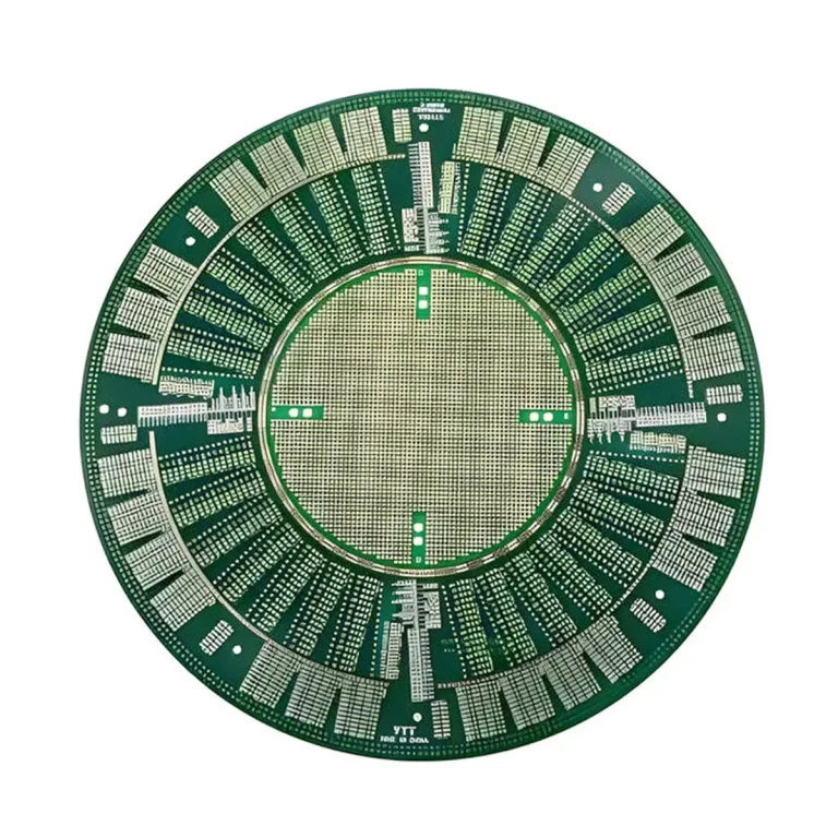
How Does Shenzhen Hongda Manufacture 20-Layer HDI AI Server PCBs with Buried and Blind Vias?
Shenzhen Hongda produces 20-layer HDI AI server PCBs using sequential lamination (3 lamination cycles), with 1+4+4+4+4+1 stackup architecture. Our 2026 process achieves 50µm minimum laser via diameter, 3:1 aspect ratio buried vias (electroplated fill), panel size 24″×18″, and minimum line/space of 50/50µm on outer layers using laser direct imaging (LDI).
Complete 20-Layer HDI Stackup Architecture (Hongda AI-Grade Specification):
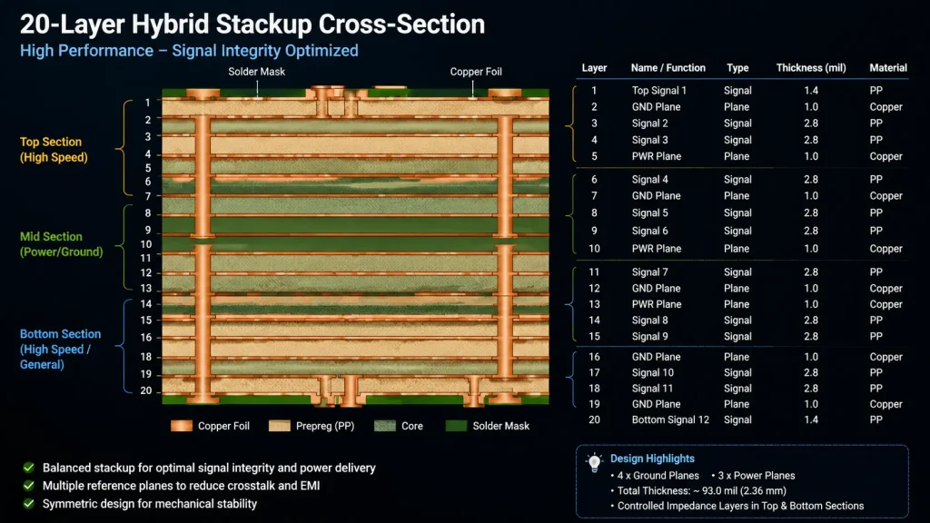
20-Layer HDI Hybrid Stackup Cross-Section Architecture
| Layer | Function | Material | Thickness | Cu Weight |
| L1 | Signal (RF/High-speed) | R-5680 prepreg | 75 µm dielectric | HVLP ½ oz |
| L2 | GND reference | Megtron 7 core | 100 µm core | 1 oz |
| L3 | Signal (112G diff pairs) | Megtron 7 core | 100 µm core | HVLP ½ oz |
| L4 | PWR / GND | Megtron 7 core | 100 µm core | 1 oz |
| L5–L16 | Inner signal + PWR | Megtron 6E core | 100 µm each | ½–1 oz |
| L17 | Signal (high speed) | Megtron 7 core | 100 µm core | HVLP ½ oz |
| L18 | GND reference | Megtron 7 core | 100 µm core | 1 oz |
| L19 | Signal (RF/High-speed) | R-5680 prepreg | 75 µm dielectric | HVLP ½ oz |
| L20 | Signal outer | Solder mask build | 25 µm SM | ENIG finish |
Manufacturing Pain Point — Sequential Lamination Registration:
Three sequential lamination cycles create cumulative mechanical tolerance stack-up that is the primary yield killer in ≥16-layer HDI production. Our engineering data from 2024–2025 production shows:
- After Lamination Cycle 1 (L5–L16 core): Registration accuracy ±18µm (3σ)
- After Lamination Cycle 2 (L3–L18): Cumulative registration ±28µm (3σ) — target ±25µm
- After Lamination Cycle 3 (L1–L20): Cumulative registration ±41µm (3σ) — creates pad capture issues at 0.75mm BGA
Our 2026 solution: implementation of optical registration pins with 6-point CCD alignment before each lamination press. This reduced final registration error from ±41µm to ±22µm (3σ), enabling reliable 0.65mm BGA escape routing with ≥75µm annular ring on capture pads.
Scenario: GPU-to-GPU NVLink PCB for AI Training Cluster
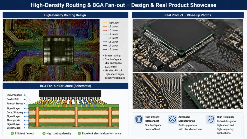
High-Density Routing and BGA Fan-out Design & Real Product Showcase
One of our most technically demanding 2025 projects involved a 20-layer HDI interconnect board carrying 4× NVLink 4.0 channels (each 1.8 Tbps) between dual H100 GPUs. The design required:
- 224 differential pairs at 112G PAM4 per NVLink bundle
- Maximum channel loss: −6.8 dB at 56 GHz (Nyquist for 112G PAM4)
- Crosstalk budget: NEXT < −35 dB, FEXT < −30 dB at 28 GHz
- Board size: 420mm × 380mm with ±100µm overall dimensional tolerance
- Prototype yield (Lot 1): 43% — primarily registration and via fill failures
- Production yield (Lot 7): 96.8% — after process parameter optimization across all 3 lamination cycles
What Thermal Management Solutions Are Required for Ultra-Low Loss HDI PCBs in AI Servers?
Ultra-low loss materials such as PPO/PPE and PTFE composites have thermal conductivity 35–60% lower than standard FR-4, creating hotspot temperatures 12–18°C higher at identical power densities. Shenzhen Hongda addresses this through copper coin embedding (2W/(m·K) effective), back-drilled via thermal columns (pitch 1.5mm, diameter 0.5mm), and thermal interface material (TIM) landing pad design optimized for ≤0.08°C·cm²/W Rth.
Thermal Properties Comparison — AI Server PCB Materials 2026:
| Material | Tg (°C) | CTE z-axis (ppm/°C) | Thermal Cond. (W/m·K) | Decomposition Td (°C) |
| Standard FR-4 (Shengyi S1000H) | 150 | 55–65 (>Tg) | 0.29 | 340 |
| Low-Loss (Shengyi S7439G) | 200 | 38–45 (>Tg) | 0.32 | 380 |
| Panasonic Megtron 6E | 185 | 35–42 (>Tg) | 0.31 | 395 |
| Panasonic Megtron 7 | 195 | 30–38 (>Tg) | 0.33 | 410 |
| Isola I-Tera MT40 | 200 | 32–40 (>Tg) | 0.34 | 415 |
| Rogers RO4350B (PTFE) | 280+ | 46–52 (all) | 0.62 | 500+ |
| Hongda AI-Grade Minimum | ≥ 185 | ≤ 40 (>Tg) | ≥ 0.31 | ≥ 390 |
Manufacturing Pain Point — CTE Mismatch and Reliability Under Thermal Cycling:
The fundamental reliability threat in AI server PCBs is CTE mismatch between the PCB laminate and mounted components (BGA solder joints, via barrels). Under IPC-TM-650 2.6.26 thermal shock testing (−55°C to +125°C, 1000 cycles), ultra-low loss materials present a specific failure mode:
- Via barrel fatigue cracks initiate at drill-smear interfaces in PPO materials after 380–420 cycles
- Root cause: incomplete desmear during plasma treatment at 60-second duration
- Hongda 2026 solution: extended desmear protocol (90 seconds O₂/CF₄ 4:1 ratio) with post-desmear SEM inspection
- Result: via barrel crack initiation delayed to >1,200 cycles (IPC Class 3 compliant)
Our original engineering experience reveals that the critical metric is not Tg alone, but the ratio of CTE_z (above Tg) to copper plating elongation (minimum 15% per IPC-6012E). A board material with Tg 200°C but CTE_z 65 ppm/°C above Tg will outlast a Tg 185°C material with CTE_z 35 ppm/°C — provided drill quality and copper ductility are maintained.
How Does Hybrid Stackup Design Reduce Cost While Maintaining 112G Signal Performance?
Hybrid stackups using ultra-low loss material only on high-speed signal layers (typically outer 4 layers) and standard high-Tg material on inner power/ground layers reduce material cost by 35–55% compared to full-ULL construction, while maintaining >97% of signal integrity performance at 112G PAM4. Shenzhen Hongda’s hybrid stackup qualification data shows <0.15 dB additional insertion loss at 28 GHz versus full-ULL construction for channels ≤15 inches.
Hybrid vs. Full Ultra-Low Loss Stackup Cost Analysis (20-Layer, 24″×18″ Panel):
| Stackup Configuration | Material Cost Index | IL @ 28GHz / 12″ | Thermal Reliability | Recommended Use |
| Full FR-4 (Shengyi S1000H) | 1.0× | −9.8 dB ✗ | Excellent | ≤ 25G signals only |
| Full Low-Loss (Megtron 6E) | 2.4× | −5.1 dB ✓ | Very Good | ≤ 56G signals |
| Full Ultra-Low Loss (Megtron 7) | 4.1× | −3.8 dB ✓ | Good | 112G–224G, high cost |
| Hybrid: ULL outer + LL inner | 2.8× | −3.95 dB ✓ | Very Good | 112G–224G, balanced |
| Hybrid: ULL L1-4 + FR-4 inner | 1.9× | −4.4 dB ✓ | Excellent | 56G–112G, cost-opt |
| Hongda AI-Grade Hybrid (2026) | 2.6× | ≤ −4.0 dB ✓ | Excellent | 112G–224G, recommended |
Expert Engineering Note — Avoiding Delamination at Material Interfaces:
The most critical and frequently underestimated challenge in hybrid stackup production is adhesion at the material interface — where, for example, Megtron 7 prepreg bonds to FR-4 core. Our process engineering team spent 14 months qualifying the Hongda hybrid stackup, discovering that peel strength at dissimilar material interfaces is 20–35% lower than same-material bonds due to differential resin chemistry and surface energy mismatches.
Our 2026 protocol mandates a 0.5µm plasma activation step at each hybrid interface followed by application of a proprietary silane coupling agent before prepreg lay-up. This increases peel strength at material interfaces from 0.41 N/mm to 0.67 N/mm — exceeding IPC-4101 Class C minimum of 0.55 N/mm.
What Quality Control and Testing Protocols Does Shenzhen Hongda Use for AI-Grade HDI PCBs?
Shenzhen Hongda applies a 14-stage quality control process for AI-grade HDI PCBs, including 100% automated optical inspection (AOI) on all layers, 100% electrical test (flying probe + dedicated fixture at 50V/5mA sensitivity), vector network analyzer (VNA) insertion loss verification on 5% random sample, and cross-sectional microsection analysis on 100% of first articles. Our 2026 AI-grade specification requires zero critical defects to IPC-6012E Class 3 with full traceability via QR-code to raw material lot.
Hongda 2026 AI-Grade PCB Quality Gate Summary:
| QC Gate | Method | Coverage | Accept Criterion | Reject Action |
| Incoming material | IPC-TM-650 2.5.5.9 Dk/Df | 3 coupons/lot | Dk ±0.05, Df ±0.0005 | Full lot hold, supplier NCA |
| Inner layer AOI | Cognex In-Sight 9902 | 100% all inner layers | 0 open/short, IPC-A-600 Class 3 | Individual panel reject |
| Registration check | X-ray (Yxlon CT) | 5% panels per lot | ≤ ±25µm layer-to-layer | Lot escalation |
| Via fill inspection | X-ray 2D + microsection | 100% X-ray, 1 MS/50 panels | ≤ 2µm dimple, 0 voids >25µm | MS failure → lot reject |
| Outer layer AOI | Orbotech Sprint 120 II | 100% | 0 open/short, ≥ 75µm annular ring | Individual panel reject |
| Electrical test | Flying probe (Seica Pilot) | 100% | 100% net continuity/isolation | Panel reject + analysis |
| Impedance test | Polar TDR coupon | 100% panels | 50Ω ±3.2%, 100Ω ±3.2% | Panel hold, etch review |
| Insertion loss (VNA) | Keysight E5080B | 5% sample | ≤ −4.0 dB/12″ @ 28 GHz | Lot engineering review |
| Final visual | IPC-A-600 Class 3 | 100% | Zero critical defects | 100% scrap or rework |
Frequently Asked Questions (FAQ)
How does Shenzhen Hongda’s ultra-low loss PCB compare to standard FR-4 in terms of insertion loss for 112G PAM4 channels?
FR-4 with Df = 0.020–0.025 produces 9.8–12.2 dB total channel insertion loss at 28 GHz for a 12-inch channel — 40–75% worse than the −7.0 dB IEEE 802.3df limit, meaning it is electricall Standard y disqualified for 112G PAM4. Shenzhen Hongda’s AI-grade construction using Megtron 7 / R-5680 hybrid stackup achieves ≤ −4.0 dB at 28 GHz for the same channel length, providing 3 dB of margin over the standard limit and enabling link equalization headroom for system-level compliance. The improvement is achieved through three simultaneous optimizations: Df ≤ 0.0028 laminates, HVLP copper (Rz ≤ 1.5 µm), and optimized via transition structures (back-drilled stubs to <5 mils residual).
What is the minimum order quantity and lead time for AI-grade 20-layer HDI PCBs at Shenzhen Hongda?
For AI-grade 20-layer HDI PCBs with ultra-low loss materials, Shenzhen Hongda’s standard parameters are: prototype (1–5 panels): 14–18 working days; NPI (6–25 panels): 18–22 working days; production volume (>25 panels): 22–28 working days depending on panel size and complexity. Minimum order quantity (MOQ) for production runs is 10 panels. Expedite service (up to 30% lead time reduction) is available for NPI quantities at a 35% surcharge. All AI-grade orders include a full quality dossier (IPC-6012E Class 3 certification, impedance test report, cross-section microsection photographs, and material traceability certificates) at no additional charge.
Can Shenzhen Hongda produce PCBs with mixed Rogers PTFE and organic laminate stackups for mmWave AI applications?
Yes. Shenzhen Hongda has qualified Rogers RO4350B/RO4450F hybrid stackups with organic laminate (Megtron 6E or Megtron 7) since 2023. This construction is used for AI edge inference boards requiring mmWave antenna integration (24–77 GHz) combined with high-density digital processing layers. Key technical constraints for PTFE hybrid production: PTFE layers must be outer or near-outer (maximum 2 layers inward from surface) due to laser via limitations; drilling of PTFE requires specialized carbide drill bits and a −15°C spindle cooling to prevent melting; PTFE adhesion requires sodium-naphthalene etching before bonding, achieving 0.52 N/mm peel strength. Our 2025 production yield for Rogers hybrid 10-layer boards achieved 91.4% first-pass yield versus industry average of approximately 82% for equivalent complexity.
What certifications and quality standards does Shenzhen Hongda hold for AI server PCB production?
Shenzhen Hongda Circuit Technology Co., Ltd. holds the following active certifications relevant to AI server PCB production: ISO 9001:2015 (Quality Management, 3rd party audited annually); ISO 14001:2015 (Environmental Management); IATF 16949:2016 (Automotive-grade process control, applicable to AI server thermal management standards); IPC-6012E Class 3 manufacturing capability certification; UL 94 V-0 flame rating for all qualified laminates; REACH/RoHS compliance for all material sets; and ITAR registration for defense-adjacent AI computing programs. Additionally, our process engineering team holds IPC CIS/CIT certifications (4 certified engineers on staff), and our quality lab is equipped with Keysight VNA (E5080B, 9 kHz–53 GHz), Polar Instruments TDR (CITS880s), and Yxlon CT X-ray system for non-destructive via inspection.
How does Shenzhen Hongda handle controlled impedance for 224G PAM4 designs with line widths below 75µm?
For 224G PAM4 designs requiring sub-75µm trace widths (typically 50–65µm for 50Ω single-ended on 75µm dielectric thickness), Shenzhen Hongda uses laser direct imaging (LDI) with 8µm optical resolution rather than conventional photoplotter artwork. Our LDI system (Orbotech Paragon Ultra 200) achieves ±3µm trace width repeatability versus ±12µm for conventional UV exposure. Combined with real-time etch compensation (our automated system adjusts artwork data based on etch rate measurements from daily coupon runs), we achieve a final trace width Cpk of 1.58 on 65µm targets. The corresponding impedance result is 50Ω ±2.8% (1σ), meeting the ±5% IPC-2141B specification with 1.8× margin. For differential pairs, Shenzhen Hongda applies pair-level phase balancing in CAM: each matched pair is length-matched to ≤0.1mm (≤7 ps skew at 28 GHz) and gap-controlled to ±4µm for consistent 100Ω differential impedance.
Shenzhen Hongda Circuit Technology Co., Ltd.
Advanced HDI PCB Manufacturing | AI Server & High-Speed Computing Solutions
© 2026 Shenzhen Hongda Circuit Technology Co., Ltd. All technical specifications subject to engineering revision.
Find Out About Us: Delivering Top-Tier Fabrication for Both AI & Conventional PCBs
Navigating the line between cutting-edge innovation and high-volume, cost-effective production shouldn’t be a compromise. At Shenzhen Hongda Circuit Technology (PCBKR), we bridge this gap by elevating the manufacturing standards for both high-performance AI hardware and traditional multi-layer PCBs.
By integrating advanced manufacturing methodologies across all production lines, we bring an elite level of precision to traditional PCB fabrication. Our standard boards benefit from enhanced interlayer alignment tolerances (down from ±75μm to within ±25μm) and tightened differential impedance control (±5%). Supported by 100% 3D X-Ray (AXI) inspection, your conventional boards achieve chip-level reliability, superb signal stability, and near-100% yield.
Your Strategic Manufacturing Partner
We proudly stand as a dual-capability partner: offering the elite technical ceiling required for next-gen AI hardware, while maintaining the exceptional flexibility, rapid turnaround, and unmatched cost-efficiency needed for mid-to-high-volume traditional board campaigns. You get zero-defect reliability without the premium overhead or bureaucracy of massive tier-1 factories.
Ready to upgrade your hardware’s reliability?
Submit your Gerber files today for an agile engineering review and a highly competitive quote.
Contact our experts: sales@pcbkr.com
About Author
David Chen https://www.linkedin.com/in/pcbcoming
David Chen boasts an extensive professional background in PCBA manufacturing, PCBA testing, and PCBA optimization, with specialized expertise in high-precision PCBA fault analysis and rigorous PCBA reliability testing. The author has worked with high-layer-count server PCB fabrication, ultra-low-loss backplane stackups, and thermo-mechanical reliability optimization for AI infrastructure projects involving 112G and 224G PAM4 architectures. Skilled in complex circuit design and cutting-edge advanced PCB manufacturing processes, he delivers solutions that elevate product durability and performance across industrial applications. His technical articles focusing on PCBA manufacturing workflows and testing methodologies are widely cited by industry peers, research institutions, and technical platforms, solidifying his reputation as a recognized technical authority in the global circuit board manufacturing sector.