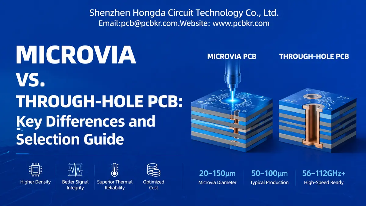
Microvia vs. Through-Hole PCB: Key Differences and Selection Guide
When procurement teams and hardware engineers search for microvias pcb solutions, they are often at a crossroads: stick with the familiar through-hole technology or migrate to laser-drilled microvias. The choice is not merely a matter of miniaturization—it directly impacts signal integrity, manufacturing cost, thermal reliability, and whether your design can support next-generation AI server or automotive ADAS architectures.
This guide breaks down the fundamental differences between pcb microvia technology and conventional through-hole construction, providing a clear decision framework for B2B buyers sourcing advanced interconnects in 2026.
What Is a PCB Microvia?
A pcb microvia in High-Density Interconnect (HDI) Microvia PCB Manufacturing | mSAP & SAP Capabilities for AI Server and HPC Applications is defined by IPC-6012 as a blind or buried interconnect with a maximum diameter of 150 μm (0.006 inches). In production environments at leading microvias pcb manufacturers, hole diameters now routinely fall in the 50–100 μm range, with advanced femtosecond laser systems achieving 20–30 μm at aspect ratios exceeding 15:1.
Unlike mechanical drilling, laser ablation removes dielectric material through photochemical decomposition. This enables:
- Hole densities up to 500,000 holes/m² on large-format panels
- ±5 μm positioning accuracy, critical for fine-pitch BGA landing pads
- Depth-controlled blind via formation without penetrating subsequent layers
- Clean hole walls with minimal resin smear
In contrast, a through-hole via is drilled mechanically through the entire board thickness, connecting all layers from top to bottom. It is robust, cost-effective, and mechanically strong—but electrically and spatially inefficient for high-density designs.
Key Differences at a Glance
| Parameter | Through-Hole PCB | Microvia PCB |
|---|---|---|
| Drilling Method | Mechanical drill bits (≥200 μm) | UV/CO₂ or femtosecond laser (50–150 μm) |
| Layer Connection | All layers (top-to-bottom) | Blind, buried, or stacked layer pairs |
| Pad Diameter | 400–600 μm | 200–350 μm |
| Via Stub | Full board thickness (stub resonance risk) | Controlled depth (minimal stub) |
| Routing Density | Lower; consumes more layers | Higher; frees routing channels |
| Signal Integrity | Adequate for <10 GHz | Optimized for 56–112 GHz+ |
| Thermal Reliability | High; proven over decades | High; requires copper fill for stacked configs |
| Relative Cost | 1.0× baseline | 1.5–3.0× depending on stackup |
| Best Application | Standard multilayer, power boards | AI servers, smartphones, HDI, RF |
Structural Architecture: Why Microvias Enable Higher Density
Through-Hole Limitations
A through-hole via creates a “stub”—the portion of the via barrel that extends beyond the signal path. In a 1.6 mm board, this stub can exceed 800 μm. At 224G PAM4 data rates (56 GHz Nyquist), this stub acts as an unterminated transmission line, producing resonant nulls that destroy channel operating margin.
Additionally, through-holes require larger pads and antipads, consuming valuable routing space on every layer. For a 0.35 mm pitch BGA, through-hole escape routing often demands two to four additional signal layers compared to a microvia-in-pad (VIP) approach.
Microvia Advantages
A blind microvia connecting L1→L2 has a stub length of roughly 100 μm—moving resonance beyond 100 GHz. Microvia pads can be as small as 200 μm, reducing parasitic capacitance by 60–70% versus mechanical via pads.
By placing the microvia directly under the BGA pad (Via-in-Pad Plated Over, or VIPPO), trace escape routing is eliminated entirely. This is why AI server GPU carrier boards and 5G-Advanced baseband units rely on microvia technology as a non-negotiable foundation.
Manufacturing Process: Subtractive vs. Semi-Additive
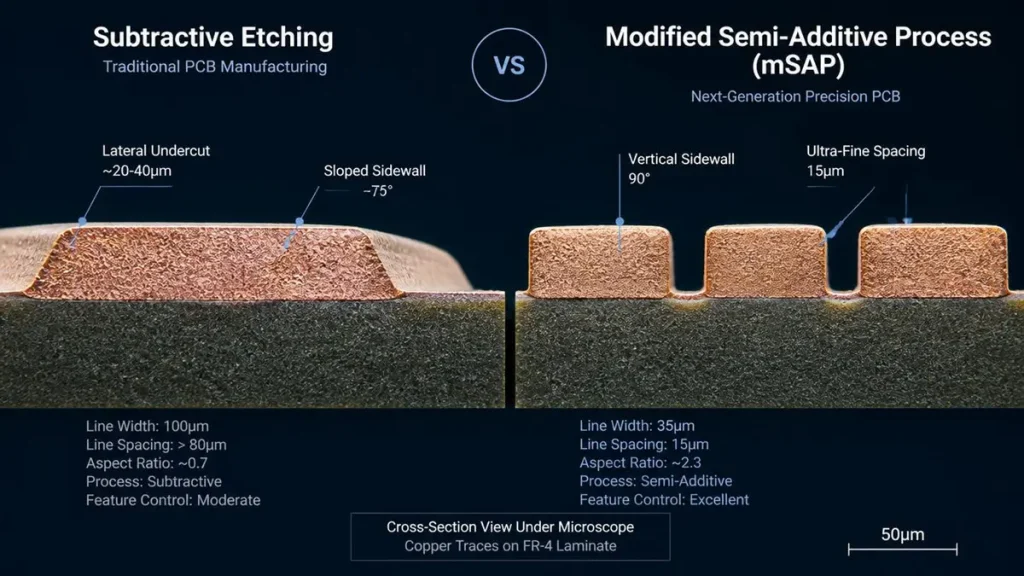
mSAP vs Subtractive Etching PCB Trace Profile – Shenzhen Hongda Circuit Technology
Through-hole PCBs are typically fabricated using subtractive etching, starting with 18–35 μm copper foil. This is mature and cost-effective for line/space dimensions above 50 μm.
However, as pcb microvia designs push trace widths below 30 μm, isotropic etching undercut becomes uncontrollable. A 5 μm variation in trace width can shift characteristic impedance by 2–3 Ω—unacceptable for 224G PAM4 channels.
This is why advanced High-Density Interconnect (HDI) Microvia PCB Manufacturing production has migrated to mSAP (Modified Semi-Additive Process):
- Laminate 1.5–3 μm ultra-thin copper seed layer
- Image trace pattern with Laser Direct Imaging (LDI) at ±1.5 μm accuracy
- Selectively plate copper to target height (15–20 μm)
- Flash-etch the thin seed layer between traces
The result is near-vertical trace sidewalls with minimal undercut, enabling 15–30 μm line/space in mass production and ±5% impedance control across the panel.
At Shenzhen Hongda Circuit Technology, our mSAP line has qualified 8 μm/8 μm line/space for substrate-like PCB (SLP) builds, while our standard production holds 20 μm/20 μm for smartphone and AI edge applications.
Reliability Considerations
Thermal-Mechanical Stress
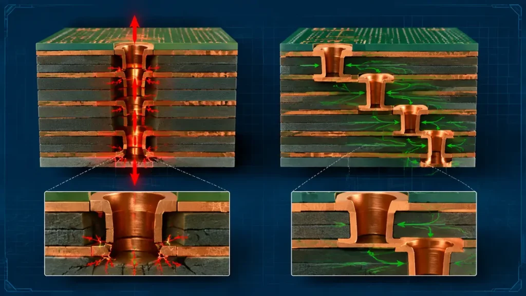
FEA thermal-mechanical stress analysis comparing Stacked Microvias (left: Z-axis stress concentration with cracking risk) and Staggered Microvias (right: evenly distributed stress in optimized HDI stackup).
AI server environments subject PCBs to continuous operating temperatures of 85–105°C, with thermal cycling from power-state transitions. A microvia with incomplete copper plating or voids in the filled barrel will fail through barrel cracking or pad lift.
For high-reliability applications, copper-filled microvias are mandatory. Our plating line achieves void-free copper fill at aspect ratios up to 20:1, verified by:
- 100% 3D X-Ray inspection (AXI) with 5% void detection sensitivity
- Microsection analysis per IPC-TM-650 2.1.1 on every production lot
- Thermal shock testing (–65°C to +150°C, 1000 cycles) for AI server qualification
When Through-Holes Still Win
Through-hole vias remain the correct choice for:
- Heavy copper power boards (4–20 oz copper) where mechanical strength is paramount
- Standard multilayer designs (4–8 layers) with generous routing space
- Cost-sensitive consumer electronics where signal integrity requirements are modest
- Applications requiring easy rework or hand soldering
Procurement Decision Framework
Specify Through-Hole If:
- Your design operates below 10 GHz and uses standard FR-4 material
- Layer count is ≤8 and BGA pitch is ≥0.8 mm
- Unit cost is the primary constraint
- The board carries high current requiring thick copper barrels
Specify Microvia If:
- You are routing 112G/224G PAM4 or PCIe Gen6 signals
- BGA pitch is ≤0.35 mm and escape routing is constrained
- You need to reduce layer count without sacrificing density
- The product operates in thermally challenging environments (AI servers, automotive under-hood, aerospace)
Hybrid Approach (Recommended for AI Servers)
For complex builds like 104-layer backplanes, the optimal strategy is hybrid:
- Blind microvias on outer layers for BGA escape routing
- Buried vias in the core for power distribution
- Back-drilled through-holes for high-speed differential pairs where stub length must be minimized to <0.2 mm
Cost Drivers: What B2B Buyers Should Know
Microvias pcb cost is driven by five factors:
- Layer count and lamination cycles — Each additional lamination stage adds 15–25% to processing cost.
- Microvia density — Higher hole densities require slower laser drilling speeds.
- Aspect ratio — Ratios above 12:1 require specialized plating chemistry.
- Material grade — M8/M9 ultra-low-loss laminates cost 3–5× standard FR-4.
- Surface finish — ENEPIG and hard gold add premium over standard ENIG or OSP.
DFM optimization tip: Consolidate microvia sizes to reduce laser setup changes, more cost-saving and fast prototyping strategies are listed in Custom Microvia PCB Fabrication & Quick-Turn HDI Prototyping: A 2026 Procurement Decision Framework. Avoid stacked microvias unless copper filling is specified. These decisions can reduce unit cost by 20–30% without compromising functionality.
Conclusion
The shift from through-hole to High-Density Interconnect (HDI) Microvia PCB Manufacturing technology is not a trend—it is a structural requirement for 2026 electronics. AI server clusters, autonomous driving platforms, and 5G-Advanced infrastructure demand the routing density, signal integrity, and thermal reliability that only laser-drilled microvias can deliver.
That said, through-hole technology retains its place in heavy copper, low-frequency, and cost-optimized applications. The key is matching the via technology to the electrical and mechanical requirements of your specific program.
At Shenzhen Hongda Circuit Technology Co., Ltd., we manufacture both through-hole multilayers and advanced microvias pcb assemblies up to 104 layers, with full mSAP capability down to 8 μm/8 μm line/space and 224G PAM4 signal integrity qualification. Whether you need a standard 6-layer control board or an Any-Layer HDI AI accelerator substrate, our engineering team provides complimentary DFM reviews with 24-hour turnaround.
Ready to optimize your next PCB design?
- Email: sales@pcbkr.com
- Engineering: pcb@pcbkr.com
- Phone: +86 0755 23720053
- Website: www.pcbkr.com
Submit your Gerber files and stackup requirements today for a complimentary DFM review and detailed quotation within 30 minutes.
FAQ: Microvia PCB Procurement
How do microvias impact overall PCB fabrication yield and cost structure?
Microvias introduce additional sequential lamination cycles, laser drilling passes, and specialized copper filling steps,
increasing base fabrication costs by 40% to 150% compared to standard multilayer boards. However, by significantly
increasing routing density, microvias often allow engineers to reduce total board layer counts (e.g., from 16 layers down to
12 layers) or shrink total PCB footprint, which offsets raw material expense and restores net program yield.
What key technical qualifications should buyers verify before selecting a microvia PCB supplier?
Procurement buyers should audit suppliers for: (1) Laser drilling equipment capability (UV/CO2 or femtosecond lasers for
sub-75 μm holes), (2) Microvia copper filling line capabilities (void-free copper plating per IPC-6012 Class 3), (3) In-house
mSAP capability with LDI registration within ±2 μm, and (4) Advanced reliability test equipment, including 3D Automated
X-ray Inspection (AXI) and microsection analysis facilities.
What are the main quality risks associated with stacked microvias versus staggered microvias?
Stacked microvias (vias directly placed atop one another across multiple layers) experience cumulative thermal expansion
stress along the Z-axis, which can cause microvia barrel cracking or interface separation during thermal reflow cycles if
copper filling is incomplete. Staggered microvias distribute thermo-mechanical stress across dielectric layers and offer
superior thermal cycling reliability, making them the preferred choice for automotive and aerospace applications unless
space constraints strictly dictate stacked structures.
How can engineering and procurement teams optimize DFM to reduce microvia manufacturing costs?
Cost-effective DFM strategies include standardizing microvia drill diameters across all layers to reduce laser head tool-
change cycles, maintaining aspect ratios at or below 1:1 (hole depth to diameter) to prevent complex plating chemistry
requirements, avoiding unnecessary stacked microvia requirements where staggered layouts fit, and utilizing industry-
standard low-loss laminates rather than exotic custom materials unless required for channel loss budgets.
What documentation is required when submitting an HDI microvia RFQ to ensure an accurate quote?
A complete quotation package must include: Gerber 274X/ODB++ files, a controlled stackup diagram detailing dielectric
thickness and copper weights, IPC classification requirement (Class 2 vs. Class 3), microvia structure definitions (blind,
buried, stacked, or staggered), microvia copper fill requirements (e.g., VIPPO / IPC-4761 Type VII), and surface finish
specifications (ENIG, ENEPIG, or Immersion Silver).
About Author
David Chen https://www.linkedin.com/in/pcbcoming
David Chen boasts an extensive professional background in PCBA manufacturing, PCBA testing, and PCBA optimization, with specialized expertise in high-precision PCBA fault analysis and rigorous PCBA reliability testing. The author has worked with high-layer-count server PCB fabrication, ultra-low-loss backplane stackups, and thermo-mechanical reliability optimization for AI infrastructure projects involving 112G and 224G PAM4 architectures. Skilled in complex circuit design and cutting-edge advanced PCB manufacturing processes, he delivers solutions that elevate product durability and performance across industrial applications. His technical articles focusing on PCBA manufacturing workflows and testing methodologies are widely cited by industry peers, research institutions, and technical platforms, solidifying his reputation as a recognized technical authority in the global circuit board manufacturing sector.