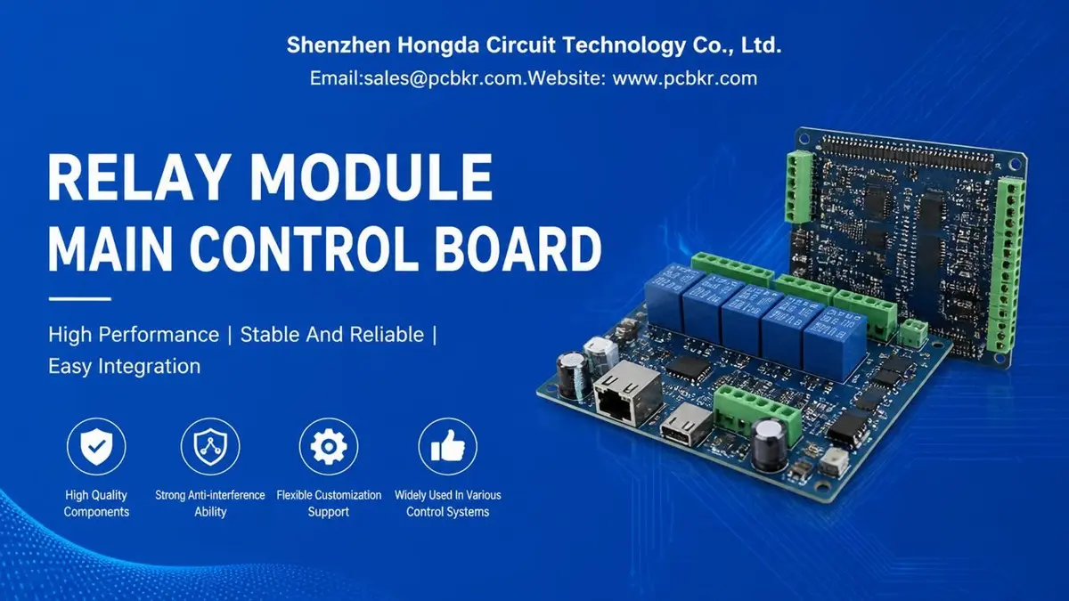
Relay Module Main Control Board Manufacturing and OEM Sourcing Guide
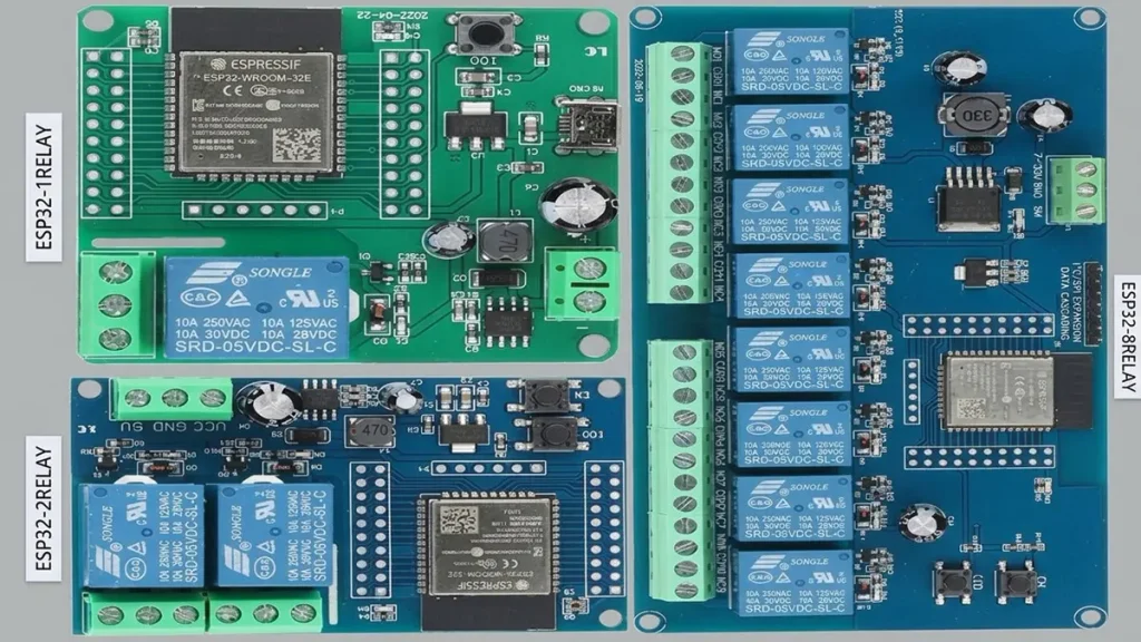
PCB Material: FR-4 / High-Tg FR-4
Quality Standard: IPC-6012
Glass Transition Temperature (Tg): According to Material Grade
Layers: 2–8 Layers
Board Thickness: 0.8–2.0 mm
Copper Thickness: 1–3 oz
Minimum Trace Width / Spacing: 0.10–0.15 mm
Minimum Hole Size: 0.20–0.30 mm
Relay Module Main Control Board – Product Details
1. Product Overview
The Relay Module Main Control Board is designed to manage relay switching, electrical load control, signal processing, and communication interfaces in industrial and embedded electronic systems. It integrates relay driver circuits, microcontroller-based control logic, power management, input/output interfaces, and electrical protection components on a customized PCB platform.
Shenzhen Hongda Circuit Technology Co., Ltd. provides customized PCB fabrication and PCBA assembly for relay module main control boards, supporting prototype development, small-batch production, and volume manufacturing.
2. Main Control Unit
- Controller Options: STM32, NXP, Microchip, Renesas, or customer-specified MCU
- Control Architecture: MCU-based centralized relay control
- Digital Input: GPIO, trigger input, status feedback
- Digital Output: Relay driver control signals
- Logic Voltage: 3.3 V / 5 V
- Control Functions: Relay sequencing, switching logic, timing control, and fault monitoring
- Firmware: Customer-provided firmware or project-specific development requirements
3. Relay Driver and Switching Circuit
- Relay Type: Electromechanical relay (EMR) or solid-state relay (SSR)
- Relay Configuration: SPST, SPDT, DPST, or DPDT
- Relay Channels: 1–16 channels, customizable
- Coil Voltage: 5 V / 12 V / 24 V DC
- Driver Circuit: NPN transistor, MOSFET, or integrated relay driver IC
- Coil Protection: Flyback diode, TVS diode, or other suitable suppression circuit
- Switching Control: Independent or grouped relay activation
- Load Switching: AC or DC loads, according to the selected relay specifications
4. Power Management
- Main Power Input: 5 V / 12 V / 24 V DC
- Power Conversion: DC-DC buck converter or LDO regulator
- Logic Power Rails: 3.3 V / 5 V
- Power Protection: Reverse-polarity protection, overcurrent protection, and transient suppression
- Power Filtering: Input filtering and local decoupling capacitors
- Optional Features: Independent relay coil power supply and logic power isolation
5. Electrical Isolation and Protection
- Isolation Architecture: Optocoupler, digital isolator, or relay contact isolation
- Control-to-Load Isolation: Configurable according to system safety requirements
- Protection Components: TVS, RC snubber, fuse, transient suppression devices
- Isolation Design: Creepage and clearance based on working voltage, pollution degree, insulation category, and applicable safety standards
- Grounding: Separate control and load return paths where required
- Noise Immunity: EMI filtering and PCB grounding optimization
6. Communication and Interface
- Communication Interfaces: UART, RS485, CAN, I2C, SPI
- External Control: GPIO and digital trigger interfaces
- Connector Options: Screw terminals, pin headers, board-to-board connectors, and wire-to-board connectors
- Status Indicators: Power, communication, relay activation, and fault LEDs
- Optional Functions: Modbus RTU, remote relay control, and communication diagnostics
7. PCB Manufacturing Technology
- PCB Layers: 2–12 layers or customized
- Copper Thickness: 1 oz / 2 oz / 3 oz / 4 oz
- PCB Materials: FR-4, high-Tg FR-4, and other application-specific laminates
- Surface Finishes: HASL, lead-free HASL, ENIG, OSP
- High-Current Design: Optimized copper width, copper thickness, and thermal distribution
- Isolation Structure: Customized creepage distance, clearance, and isolation slots
- Via Technology: Through-hole vias, blind vias, and buried vias according to design requirements
- Impedance Control: Available when required by high-speed communication interfaces
8. PCBA Assembly and Testing
- Assembly Technology: SMT, THT, and mixed-technology assembly
- Component Assembly: MCU, relay, MOSFET, driver IC, protection components, and connectors
- Soldering: Lead-free reflow soldering and wave/selective soldering as applicable
- Inspection: 3D AOI, X-ray inspection, and visual inspection
- Electrical Testing: Continuity, shorts, power-on, and functional testing
- Additional Testing: Relay switching verification, communication testing, and insulation testing according to project requirements
9. Typical Applications
- Industrial Automation and Control Systems
- Smart Home and Building Automation
- Industrial Relay Control Modules
- Power Distribution and Load Switching
- HVAC Control Systems
- Energy Management Equipment
- Smart Metering and Monitoring Systems
- Embedded Electrical Control Systems
Relay Module Main Control Board – Technical Data Sheet
1. Electrical Specifications
| Parameter | Specification |
|---|---|
| Main Power Input | 5 V / 12 V / 24 V DC |
| Logic Operating Voltage | 3.3 V / 5 V DC |
| Controller | STM32 / NXP / Microchip / Custom MCU |
| Relay Type | EMR / SSR |
| Relay Channels | 1–16 channels |
| Relay Coil Voltage | 5 V / 12 V / 24 V DC |
| Relay Contact Configuration | SPST / SPDT / DPST / DPDT |
| Switching Voltage | AC / DC, relay-dependent |
| Switching Current | 1–16 A, relay-dependent |
| Driver Type | MOSFET / Transistor / Driver IC |
| Input Interface | GPIO / Digital Trigger |
| Output Interface | Relay Contacts / Status Signals |
| Power Conversion | DC-DC / LDO |
2. Communication Specifications
| Parameter | Specification |
|---|---|
| UART | Optional |
| RS485 | Optional |
| CAN | Optional |
| I2C | Optional |
| SPI | Optional |
| Modbus RTU | Optional |
| Communication Speed | Project-dependent |
| External Connector | Terminal Block / Pin Header |
| Status Indicator | Power / Relay / Communication / Fault |
3. Protection and Isolation Specifications
| Parameter | Specification |
|---|---|
| Input Protection | Reverse Polarity / Overcurrent |
| Transient Protection | TVS / Surge Suppression |
| Relay Coil Protection | Flyback Diode / TVS |
| Output Protection | Fuse / RC Snubber / TVS |
| Electrical Isolation | Optocoupler / Digital Isolator / Relay |
| Creepage Distance | Customized according to safety requirements |
| Clearance Distance | Customized according to safety requirements |
| Grounding | Single Ground / Separated Ground Architecture |
| EMI Protection | Optional |
4. PCB Fabrication Specifications
| Parameter | Specification |
|---|---|
| PCB Layers | 2–12 Layers |
| PCB Material | FR-4 / High-Tg FR-4 |
| Copper Thickness | 1–4 oz |
| Board Thickness | 0.8–2.0 mm, customizable |
| Minimum Line Width/Spacing | According to design and manufacturing requirements |
| Surface Finish | HASL / ENIG / OSP |
| Solder Mask | Green / Blue / Black / White |
| Silkscreen | White / Black |
| Via Structure | Through / Blind / Buried Via |
| Impedance Control | Optional |
| High-Current Copper Design | Customized |
5. PCBA Assembly Specifications
| Parameter | Specification |
|---|---|
| Assembly Process | SMT / THT / Mixed Assembly |
| Component Types | MCU / Relay / MOSFET / IC / Connector |
| Soldering Process | Reflow / Wave / Selective Soldering |
| Inspection | 3D AOI / X-ray / Visual Inspection |
| Electrical Testing | Continuity / Short Circuit / Power-On |
| Functional Testing | Relay Switching / I/O / Communication |
| Programming | Optional |
| Conformal Coating | Optional |
| Final Assembly | Optional |
6. Environmental and Reliability Requirements
| Parameter | Specification |
|---|---|
| Operating Temperature | Project-dependent |
| Storage Temperature | Component-dependent |
| Operating Humidity | Application-dependent |
| Thermal Management | Copper Optimization / Thermal Relief |
| Mechanical Reliability | Relay and Connector Dependent |
| Electrical Endurance | Relay Manufacturer’s Rated Switching Life |
| EMC Testing | According to Product Requirements |
| Insulation Testing | According to Applicable Safety Standards |
7. Manufacturing and Quality Control
| Parameter | Specification |
|---|---|
| PCB Fabrication | Prototype / Small Batch / Mass Production |
| PCB Inspection | AOI / Electrical Testing |
| PCBA Inspection | 3D AOI / X-ray |
| Electrical Verification | Flying Probe / Functional Testing |
| Component Sourcing | Customer-Supplied / Turnkey |
| Production Documentation | Inspection and Quality Records |
| Quality Standards | Applicable IPC Requirements |
| Manufacturing Support | DFM / DFA / Engineering Review |
A reliable Relay Module Main Control Board requires more than selecting suitable relays and connecting control signals. Its performance depends on relay selection, PCB current-carrying capacity, electrical isolation, driver protection, thermal management, and reliable PCBA assembly. For OEM buyers, choosing a manufacturer with integrated PCB fabrication, component sourcing, assembly, and testing capabilities helps reduce production risks and maintain consistent product quality.
Shenzhen Hongda Circuit Technology Co., Ltd. provides custom PCB manufacturing and PCBA assembly services for industrial control electronics, including relay-based control boards. From prototype development to small-batch and volume production, manufacturing requirements can be coordinated according to the customer’s electrical specifications, PCB design, component selection, and assembly requirements.
1. Relay Module Main Control Board Structure and Applications
A Relay Module Main Control Board is an electronic control assembly that uses relay devices to switch electrical loads according to control signals from a microcontroller, PLC, or external control system. It provides an interface between low-voltage control circuits and the equipment being switched.
A typical relay control board consists of several functional sections:
- Main Control Unit: Processes input signals and manages relay switching operations.
- Relay Driver Circuit: Controls relay coils through transistors, MOSFETs, or dedicated driver ICs.
- Relay Switching Section: Provides electrical switching through normally open (NO) and normally closed (NC) contacts.
- Power Management Circuit: Supplies regulated power to the controller and relay coils.
- Protection Circuit: Helps protect control electronics against reverse polarity, transient voltage, and inductive switching effects.
- Input and Output Interfaces: Connects sensors, controllers, external power supplies, and controlled equipment.
Relay control boards are used in industrial automation, PLC control systems, building automation, HVAC equipment, power distribution, energy management, smart metering, and industrial machinery.
The circuit architecture varies according to the number of relay channels, load characteristics, control interface, operating environment, and system safety requirements.
2. Electrical Design Requirements for Relay Control Boards
Electrical specifications should be established before PCB layout and component sourcing. Incorrect assumptions about relay coil voltage, contact ratings, or load characteristics can lead to switching failures, excessive heating, or premature component degradation.
Relay Coil Voltage and Control Logic
Relay coil voltage and contact switching voltage are two different electrical parameters.
The coil voltage determines the power required to activate the relay. Common relay coil configurations include 5 V, 12 V, and 24 V DC, depending on the application.
The control logic voltage is the signal level used by the microcontroller or external controller. Typical logic levels include 3.3 V and 5 V.
The driver circuit must provide sufficient coil current while remaining compatible with the controller’s output capability. Directly driving a relay coil from a microcontroller GPIO pin is generally inappropriate unless the device is specifically designed to support the required current.
Relay Contact Configuration
Relay contacts determine how the switched circuit is connected.
Common configurations include:
- SPST: Single Pole Single Throw.
- SPDT: Single Pole Double Throw.
- DPST: Double Pole Single Throw.
- DPDT: Double Pole Double Throw.
The appropriate contact configuration depends on the load circuit, switching function, and required isolation arrangement.
AC and DC Load Characteristics
AC and DC loads do not necessarily impose the same switching requirements.
Inductive loads, such as motors, solenoid valves, and electromagnetic actuators, can generate voltage transients during switching. Capacitive loads may produce high inrush currents when energized. Resistive loads generally have more predictable switching characteristics, but their actual current and operating temperature still need to be considered.
Relay selection should therefore account for:
- Rated switching voltage.
- Rated switching current.
- Load type and power factor.
- Inrush and transient current.
- Switching frequency.
- Expected electrical operating life.
- Ambient temperature and installation conditions.
The relay manufacturer’s datasheet should be used to verify contact ratings under the actual load conditions. A relay’s maximum resistive-load rating should not automatically be applied to motor, inductive, or capacitive loads.
3. PCB Copper Thickness and Current-Carrying Design
PCB copper thickness is an important factor in the electrical and thermal performance of a Relay Module Main Control Board. Relay output circuits may carry substantially higher currents than the low-voltage control section, requiring different routing and copper design considerations.
Copper Thickness Selection
Copper thickness affects the resistance of PCB traces and their ability to distribute heat.
Common copper configurations include:
- 1 oz copper for general control and signal circuits.
- 2 oz copper for higher-current power distribution and relay output circuits.
- 3 oz copper for selected high-current applications requiring additional copper capacity.
The appropriate copper weight depends on the actual current, trace width, copper temperature rise, PCB construction, and surrounding thermal conditions.
Trace Width and Current Capacity
PCB current capacity is influenced by several interacting factors:
- Copper thickness.
- Trace width and length.
- Allowable temperature rise.
- Ambient temperature.
- Internal or external copper location.
- Heat dissipation through the PCB and surrounding components.
A relay rated for a particular contact current does not mean that every PCB trace connected to it can safely carry the same current.
The PCB layout must also consider connector ratings, solder joint dimensions, terminal spacing, and the electrical characteristics of the connected load.
High-Current Relay Output Design
For high-current applications, the PCB design may require wider copper traces, heavier copper, larger solder pads, reinforced terminal connections, or optimized routing.
Where appropriate, copper planes or parallel copper paths can help distribute current. However, the final design must be evaluated as a complete electrical and thermal system rather than relying on copper weight alone.
Hongda Circuit supports PCB fabrication with different copper thickness configurations according to project requirements. PCB material, copper weight, layer construction, and manufacturing tolerances can be coordinated during engineering review.
4. Relay Driver Circuit Protection and Electrical Transient Control
Relay coils are inductive loads. When a relay coil is switched off, its magnetic field collapses and generates a reverse voltage that can damage driver components or interfere with nearby control circuits.
A properly designed relay driver circuit helps protect the control electronics and improve switching reliability.
Transistor and MOSFET Drivers
NPN transistors and MOSFETs are commonly used to control relay coils.
A transistor driver provides a switching interface between the controller and relay coil. A MOSFET driver can offer lower conduction losses in suitable circuit configurations.
Component selection should consider:
- Maximum coil current.
- Driver voltage rating.
- Switching frequency.
- Gate or base drive requirements.
- Power dissipation.
- Thermal operating conditions.
The driver circuit must also maintain adequate margin against voltage and current transients.
Flyback Diode Protection
A flyback diode is commonly connected across a DC relay coil to provide a current path when the driver switches off.
This limits the reverse voltage generated by the coil and helps protect the switching transistor or MOSFET.
However, a standard flyback diode can increase relay release time because the coil current decays more slowly. Where faster release is required, alternative suppression methods such as diode-Zener combinations or TVS devices may be evaluated.
TVS and Transient Protection
TVS diodes and other transient suppression components may be used to protect power inputs, control interfaces, and switching circuits.
Protection requirements depend on the power supply characteristics, wiring length, external load, switching environment, and applicable electrical standards.
Reverse-polarity protection, overcurrent protection, and power-input filtering may also be incorporated into the design.
5. Electrical Isolation Between High-Voltage and Low-Voltage Circuits
Relay modules frequently connect low-voltage control electronics to higher-voltage load circuits. Proper electrical isolation is therefore an important part of PCB design and product safety.
Creepage Distance and Clearance Distance
Creepage distance is the shortest distance between conductive parts measured along the surface of an insulating material.
Clearance distance is the shortest distance through air between conductive parts.
Both are important when designing PCB layouts that contain different voltage domains.
The required distances depend on factors such as:
- Working voltage.
- Rated impulse voltage.
- Overvoltage category.
- Pollution degree.
- Insulation type.
- PCB material group.
- Applicable product safety standards.
A universal spacing value should not be applied to every relay control board.
Optocoupler and Digital Isolation
Optocouplers and digital isolators can provide signal isolation between control and switching circuits.
The isolation component must be selected according to working voltage, transient requirements, insulation classification, and the applicable safety standard.
The PCB layout must also maintain the required separation around the isolation barrier. Component package ratings alone do not establish that the complete PCB assembly meets the required insulation conditions.
PCB Isolation Slots and Layout Separation
PCB slots may be used to increase creepage distance where the design and applicable standards permit.
Other layout considerations include:
- Separating high-voltage and low-voltage copper regions.
- Avoiding unintended copper overlap.
- Maintaining adequate spacing around terminals and relay contacts.
- Controlling solder mask openings.
- Preventing contamination across insulation barriers.
- Reviewing component placement and enclosure clearances.
For custom relay control boards, isolation requirements should be confirmed during schematic review and PCB design verification rather than left until final assembly.
6. Thermal Management for Multi-Channel Relay Boards
Thermal management becomes increasingly important when multiple relays operate simultaneously or when the board is installed in a compact enclosure.
Heat can originate from relay coils, contact resistance, PCB traces, driver components, power regulators, and connected loads.
Relay Coil and Driver Heat
Relay coils consume power whenever they are energized. Multiple active channels can increase the total heat generated on the board.
Driver transistors and MOSFETs also dissipate power during operation. Their thermal performance depends on electrical loading, switching conditions, PCB copper area, and component package characteristics.
Copper Distribution and Component Placement
PCB layout can influence heat distribution.
Design considerations include:
- Providing suitable copper area around power components.
- Avoiding excessive concentration of heat-generating components.
- Maintaining appropriate spacing between relays.
- Optimizing high-current trace routing.
- Considering thermal paths to the enclosure or mounting structure.
Operating Environment
The expected ambient temperature and enclosure conditions should be included in thermal evaluation.
A relay board operating in an open laboratory environment may experience different thermal conditions from a board installed inside a sealed industrial control cabinet.
Thermal validation should therefore reflect the intended installation environment and expected simultaneous relay operation.
7. PCB Manufacturing Technologies for Relay Control Boards
PCB fabrication quality directly affects electrical connectivity, insulation performance, mechanical strength, and long-term reliability.
Relay Module Main Control Boards may use conventional FR-4 or High-Tg FR-4 materials, depending on the operating environment and thermal requirements.
PCB Material and Layer Construction
FR-4 is widely used for industrial control boards because of its mechanical strength, electrical insulation, and established manufacturing processes.
High-Tg FR-4 may be considered for applications requiring improved thermal performance or more demanding assembly conditions.
The PCB layer structure should be determined by circuit complexity, power distribution, signal routing, grounding, and isolation requirements.
Copper Pattern Formation and Circuit Accuracy
Accurate copper pattern formation is important for maintaining trace width, spacing, and electrical connectivity.
Hongda Circuit uses SCREEN Ledia laser direct imaging (LDI) equipment, with an 8 μm target imaging capability and ±10 μm target tolerance under the specified process conditions.
The actual trace and spacing capability depends on copper thickness, board construction, design geometry, and production conditions.
Drilling and Interlayer Connections
Drilled holes and plated through-holes provide electrical connections between PCB layers.
Hole quality and copper plating consistency are important for electrical continuity and mechanical reliability.
For multilayer boards, the manufacturing process must also control layer registration, lamination, drilling, and plating to maintain reliable interconnections.
Lamination and Material Bonding
Multilayer PCB construction requires controlled lamination to bond copper layers and insulating materials.
Hongda Circuit uses LAUFFER lamination equipment with configurable pressure and vacuum conditions. The process is selected according to the material system, stackup, and production requirements.
Surface Finish and Solderability
Surface finish affects solderability, component assembly, and exposed copper protection.
Common options include:
- ENIG.
- Lead-Free HASL.
- OSP.
The appropriate finish depends on component requirements, soldering processes, storage conditions, and product application.
PCB Quality Standards
IPC-6012 is relevant to rigid printed board qualification and performance requirements. The applicable class and acceptance criteria should be agreed upon according to the product’s intended application and customer requirements.
PCB inspection may include dimensional verification, visual inspection, electrical continuity testing, and other checks specified by the fabrication drawing and purchase order.
For additional manufacturing information, buyers can review Hongda Circuit’s heavy copper PCB manufacturing capabilities and PCB assembly services.
8. PCBA Assembly Processes for Relay Control Boards
Relay control boards commonly combine surface-mount components with through-hole relays, connectors, and terminal blocks. This mixed-technology construction requires suitable assembly and soldering processes.
SMT Component Placement
SMT components may include microcontrollers, driver ICs, resistors, capacitors, protection devices, and communication components.
The SMT process typically includes solder paste printing, component placement, and reflow soldering.
Process control is important for component positioning, solder paste volume, solder joint formation, and thermal exposure.
Through-Hole Component Assembly
Relays and terminal blocks frequently use through-hole mounting because of their mechanical and electrical requirements.
Depending on component construction and board design, assembly may use wave soldering, selective soldering, or manual soldering.
Selective Soldering for Mixed-Technology Boards
Selective soldering is useful when through-hole components must be soldered on a board that also contains previously assembled SMT components.
The process helps control solder application to designated areas and reduces unnecessary thermal exposure to nearby components.
Large Component and Terminal Reliability
Relay bodies and terminal blocks can introduce mechanical stress during installation and operation.
Assembly review should consider:
- Through-hole pad dimensions.
- Annular ring requirements.
- Hole and lead compatibility.
- Solder fill and joint quality.
- Component positioning.
- Mechanical support.
- Connector insertion and removal forces.
A reliable PCBA process must address both electrical connection quality and the mechanical demands of the final application.
9. PCB Inspection and Functional Testing Before Shipment
PCB fabrication inspection and PCBA functional testing serve different purposes. Bare PCB electrical testing verifies the board’s conductive connections, while PCBA testing evaluates the assembled electronic product.
Both should be considered when defining the manufacturing quality plan.
3D AOI Inspection
3D Automated Optical Inspection (AOI) can identify visible assembly defects such as component misalignment, missing components, polarity errors, and soldering anomalies.
AOI inspection is particularly useful for SMT components and repeatable production quality monitoring.
X-Ray Inspection
X-ray inspection can be applied to solder joints that are difficult to inspect optically, depending on component package construction and joint geometry.
It may be useful for selected bottom-terminated or hidden solder connections.
Electrical Continuity Testing
Electrical tests can verify the continuity of designated circuits and identify open or short connections.
Test coverage should be based on the PCB design, netlist, and customer requirements.
Relay Coil Activation Testing
Functional testing can verify that relay coils activate correctly under the specified supply and control conditions.
The test procedure may include:
- Coil voltage verification.
- Driver circuit operation.
- Relay activation and release.
- Control input response.
- Channel switching sequence.
Output Contact Verification
The relay output should be evaluated according to the intended switching function.
Testing may verify contact continuity, normally open and normally closed states, and switching response under defined test conditions.
Where actual load switching is required, the test setup must be designed around the specified voltage, current, and load characteristics.
Insulation and Hi-Pot Testing
Insulation resistance and dielectric withstand testing may be required for boards involving hazardous voltages or safety-critical applications.
The test voltage, duration, acceptance criteria, and test configuration must follow the applicable product standard and approved customer test specification.
Not every relay board requires the same insulation test procedure.
10. RFQ Requirements for Custom Relay Module Main Control Board Manufacturing
A complete RFQ package helps manufacturers evaluate technical feasibility, component availability, manufacturing cost, and production lead time.
Buyers should prepare the following information whenever available.
| Required Information | Purpose |
|---|---|
| Gerber Files | PCB fabrication data |
| PCB Fabrication Drawing | Board dimensions, thickness, copper and finish requirements |
| Schematic | Circuit architecture and electrical connections |
| BOM | Component specifications and sourcing |
| Pick-and-Place File | SMT assembly positioning |
| Relay Datasheets | Coil and contact specifications |
| Electrical Load Specifications | Voltage, current and load characteristics |
| Testing Requirements | Functional and electrical test coverage |
| Assembly Drawings | Component orientation and mechanical requirements |
| Annual Quantity | Production planning and cost evaluation |
| Prototype Quantity | Initial engineering and sample production |
| Delivery Requirements | Production scheduling and logistics |
For projects without complete manufacturing files, buyers can provide the available schematic, reference design, technical requirements, and estimated production quantity for an initial engineering review.
Factors Affecting Manufacturing Cost
The cost of a custom Relay Module Main Control Board depends on more than PCB dimensions.
Important cost factors include:
- PCB material and layer count.
- Copper thickness.
- Board dimensions and fabrication complexity.
- Surface finish.
- Relay brand, model, and quantity.
- Electronic component sourcing.
- SMT and through-hole assembly requirements.
- Testing and inspection coverage.
- Production quantity.
- Packaging and delivery requirements.
A complete BOM and technical specification generally allow a more accurate quotation and reduce the risk of unexpected component substitutions or manufacturing changes.
11. Custom Relay Module PCB Manufacturer and OEM PCBA Support
Selecting a reliable manufacturer requires evaluating both PCB fabrication and PCBA assembly capabilities.
A supplier that understands only bare PCB production may not fully address relay selection, component compatibility, through-hole assembly, and functional testing requirements.
Hongda Circuit supports PCB manufacturing and PCBA assembly for custom industrial electronic control applications.
Integrated PCB Fabrication and PCBA Assembly
Coordinating PCB fabrication and assembly helps align board construction, component footprints, soldering processes, and inspection requirements.
This is particularly important for relay boards that combine high-current output circuits, low-voltage control electronics, and large through-hole components.
Engineering and DFM Review
Design for Manufacturability (DFM) review can help identify potential production issues before manufacturing.
The review may cover:
- PCB stackup and copper requirements.
- Trace width and spacing.
- Hole and pad dimensions.
- Component footprint compatibility.
- High-voltage isolation layout.
- Relay and terminal placement.
- SMT and THT assembly feasibility.
- Test point accessibility.
Prototype and Production Support
Prototype production helps verify board construction, component compatibility, assembly feasibility, and functional operation before volume manufacturing.
After prototype approval, the manufacturing process can be transferred to small-batch or volume production according to the approved design and quality requirements.
Quality and Production Coordination
Manufacturing quality depends on consistent process control, inspection, traceability, and clear acceptance criteria.
Hongda Circuit can coordinate PCB fabrication, component sourcing, SMT/THT assembly, and testing requirements according to the project specification.
12. Request a Quote for Relay Module Main Control Board Manufacturing
Hongda Circuit provides custom PCB and PCBA manufacturing services for industrial control and relay-based electronic products.
Whether the project requires a new relay control board, an existing design manufactured by an OEM supplier, or integrated PCB fabrication and assembly, technical requirements can be reviewed before production.
To request a quotation, please provide:
- PCB Gerber files.
- BOM and relay part numbers.
- Schematic and assembly drawings.
- Electrical load and operating requirements.
- Prototype or production quantity.
- Required testing and inspection specifications.
Our engineering and sales teams can review the submitted information and evaluate the manufacturing requirements.
Contact Shenzhen Hongda Circuit Technology Co., Ltd.
- Email: sales@pcbkr.com
- Website: www.pcbkr.com
Submit your Relay Module Main Control Board project for PCB fabrication and PCBA assembly evaluation.
Frequently Asked Questions About Relay Module Main Control Board Manufacturing
Can you manufacture custom Relay Module Main Control Boards based on customer designs?
Yes. We support custom Relay Module Main Control Board manufacturing based on customer schematics, PCB layout files, Gerber data, BOMs, and technical specifications. Our services can include PCB fabrication, component sourcing, SMT and THT assembly, and functional testing according to project requirements.
What files are required to obtain a quotation for a custom relay control board?
For an accurate quotation, please provide Gerber files, BOM, schematic, assembly drawings, relay part numbers, technical specifications, estimated order quantity, and required delivery schedule. If available, include electrical isolation requirements and applicable safety standards.
How do you prevent electrical interference and protect relay driver circuits?
The design review can evaluate relay coil switching transients, flyback diodes or TVS protection, power supply decoupling, grounding, and separation between high-current switching paths and sensitive control signals. The appropriate protection method depends on the relay type, switching load, and circuit design.
Can you support both prototype production and mass production?
Yes. We support prototype, small-batch, and volume production. PCB fabrication, component procurement, SMT/THT assembly, inspection, and functional testing can be coordinated across production stages. Design and process reviews help identify manufacturing risks before volume production.
What quality inspections and functional tests are available before shipment?
Depending on the product design and agreed inspection plan, available processes may include automated optical inspection (AOI), X-ray inspection for applicable solder joints, electrical continuity testing, insulation resistance testing, and relay switching or functional verification. Test procedures and acceptance criteria should be confirmed during engineering review.
About Author
David Chen LinkedIn Profile
David Chen is a Senior RF/PCB Process Engineer at Shenzhen Hongda Circuit Technology Co., Ltd., with over 12 years of experience in high-frequency PCB fabrication, impedance-controlled stack-up design, and Rogers/PTFE laminate processing. He also boasts an extensive professional background in PCBA manufacturing, PCBA testing, and PCBA optimization, with specialized expertise in high-precision PCBA fault analysis and rigorous PCBA reliability testing. The author has worked with high-layer-count server PCB fabrication, ultra-low-loss backplane stackups, and thermo-mechanical reliability optimization for AI infrastructure projects involving 112G and 224G PAM4 architectures. Skilled in complex circuit design and cutting-edge advanced PCB manufacturing processes, he delivers solutions that elevate product durability and performance across industrial applications. His technical articles focusing on PCBA manufacturing workflows and testing methodologies are widely cited by industry peers and technical platforms, and have gained attention and recognition from industry colleagues.