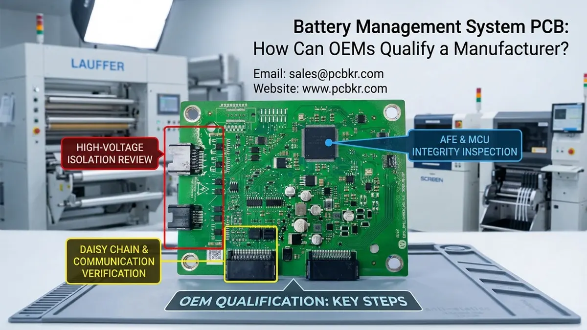
Battery Management System PCB: How Can OEMs Qualify a Manufacturer?
A reliable Battery Management System PCB starts with more than selecting a copper weight or choosing a board supplier. OEMs need a manufacturer that can review the fabrication data, understand high-current and low-level sensing requirements, control multilayer manufacturing, and provide inspection evidence appropriate to the order. Shenzhen Hongda Circuit Technology Co., Ltd. supports PCB manufacturing and PCBA assembly projects from prototype and small-batch builds to production orders. The right manufacturing scope depends on your board design, application, quality requirements, and validation plan.
What BMS PCB Manufacturing Services Does Your Project Need?
The first step is to define whether you need bare PCB fabrication, component assembly, or a combined manufacturing service. These are different scopes of work and should be identified before requesting a quotation.
For OEM projects, the required service may include:
- Custom BMS PCB fabrication: Manufacturing from customer-approved Gerber or ODB++ data, drill files, stackup requirements, and fabrication notes.
- BMS PCBA assembly: SMT and through-hole assembly according to the approved BOM, centroid data, assembly drawings, and process requirements.
- Turnkey PCBA: PCB fabrication, component sourcing where agreed, assembly, and specified inspections.
- Prototype and small-batch manufacturing: Initial builds for fit checks, assembly evaluation, and customer-led electrical or functional validation.
- Production manufacturing: Repeat orders controlled through approved files, material specifications, process requirements, and revision management.
A BMS PCB can serve an electric vehicle, an energy storage system, an industrial battery, a mobile robot, or another battery-powered product. Those applications do not necessarily share the same voltage, current, thermal, environmental, or quality requirements.
PCBKR’s role is to manufacture the board and assembly within the agreed scope. Battery algorithm development, firmware calibration, battery-pack engineering, and complete BMS system validation should be quoted separately if required and only where those services are available.
For OEM buyers looking for a manufacturing partner, start with the PCB manufacturer service page.
What BMS PCB Specifications Must Be Confirmed Before Quoting?
A useful BMS PCB quotation begins with complete technical information. A board’s layer count and dimensions alone are not enough to determine its manufacturing cost, production route, or inspection requirements.
| Specification | What the buyer should provide | Why it matters |
|---|---|---|
| Board data | Gerber or ODB++, drill files, fabrication drawing | Defines the copper pattern, holes, and board geometry |
| Stackup | Layer count, finished thickness, dielectric requirements | Determines construction and lamination requirements |
| Copper | Required finished copper thickness by layer | Supports review of current-carrying paths and fabrication feasibility |
| Electrical requirements | Working voltage, current profile, isolation requirements where applicable | Identifies constraints that may affect layout, materials, and inspection |
| Critical features | Fine-pitch components, connector footprints, via requirements, controlled impedance if specified | Helps identify manufacturing and assembly constraints |
| Surface finish | ENIG, HASL, OSP, or another approved finish | Must suit the component, soldering, contact, and storage requirements |
| Assembly data | BOM, pick-and-place file, assembly drawings, approved substitutions | Supports component sourcing, assembly planning, and quotation |
| Inspection requirements | Bare-board electrical test, AOI, X-ray, ICT, FCT, or other specified checks | Establishes what must be inspected, tested, and documented |
| Order details | Prototype quantity, expected production volume, delivery target | Affects setup, procurement, capacity planning, and cost |
For a turnkey quotation, send the BOM and assembly files as well as the PCB fabrication package. If components are customer-supplied, identify that clearly. Include any approved alternatives, special handling requirements, and restrictions on substitutions.
If some information is not yet available, state what is preliminary. An engineering review can identify missing inputs before the manufacturing specification is frozen.
How Are High-Current Paths Reviewed Before BMS PCB Manufacturing?
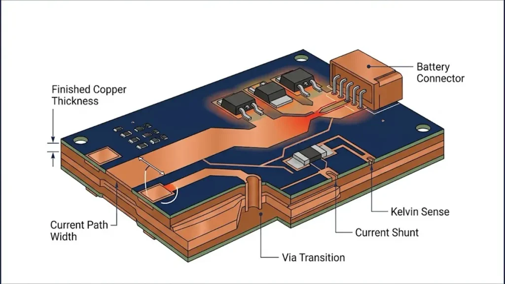
Battery Management System PCB high-current path review showing copper traces, MOSFETs, current shunt, vias, and Kelvin sensing connections.
High-current BMS designs need a review of the complete current path, not just the nominal copper weight. Copper thickness is one input among several; it does not independently establish a safe current rating.
The review should consider:
- Continuous current and peak current, including pulse duration and duty cycle.
- Required finished copper thickness and the actual width of each current-carrying segment.
- Narrow sections near connector pads, fuses, shunts, MOSFETs, and terminal blocks.
- Via count, via dimensions, layer transitions, and the path between copper layers.
- Ambient temperature, enclosure conditions, nearby heat sources, and acceptable temperature rise.
- Mechanical connections, solder-joint requirements, and the customer’s validation criteria.
A wide copper area can still contain a bottleneck where the path narrows near a component pad. Likewise, a design with substantial copper may need additional thermal evaluation if its current is concentrated in a small area.
PCBKR offers Heavy Copper PCB manufacturing for projects whose design requires increased copper thickness. The appropriate copper specification must be confirmed against the actual design and manufacturing requirements.
What does the manufacturer review, and what must the OEM validate?
A manufacturer can review fabrication feasibility, copper and layer requirements, drill and via specifications, and other visible manufacturing risks. Thermal performance, voltage drop, protection behavior, and safe operating limits must be established using the design requirements and suitable engineering calculations or tests.
For a high-current BMS PCB, ask the supplier to identify any manufacturability concerns before the files are released for production. Do not rely on a generic statement such as “2 oz copper supports high current” as a complete engineering approval.
What Should Be Checked Around BMS Current-Sensing Circuits?
Current sensing deserves particular attention because the measured signal can be small compared with the current flowing through the power path. The shunt resistor, its connections, and the sensing layout must be considered together.
Before manufacturing, check that the approved design clearly defines:
- The current-shunt footprint and specified component.
- The intended sensing connections, including Kelvin connections where required by the design.
- The relationship between the high-current path and the low-level sensing traces.
- Required clearances, copper geometry, and relevant assembly tolerances.
- Test access and any specified low-resistance measurement requirements.
The purpose of this review is to identify potential manufacturing or assembly issues, not to redesign the customer’s circuit without authorization.
PCBKR’s four-wire Kelvin flying-probe testing capability can be relevant when the project calls for suitable low-resistance measurements and the test method is applicable to the board. Four-wire measurement reduces the influence of lead and contact resistance compared with a basic two-wire measurement, but it does not by itself verify the accuracy of the complete BMS current-measurement system.
If precise resistance verification is required, agree on the measurement points, acceptance limits, test conditions, and report format before production.
Which PCB Manufacturing Technologies Matter for a BMS Board?
The best manufacturing process is the one that meets the board’s actual electrical, mechanical, and reliability requirements. A conventional BMS control board does not automatically require the most advanced fine-line PCB process. High-density imaging and microvia technology should be used when the design justifies them, rather than added simply to make a specification appear advanced.
How Does LDI Help With BMS PCB Fabrication?
Laser Direct Imaging (LDI) supports the accurate imaging of copper patterns. PCBKR’s SCREEN Ledia LDI capability has a stated 8 µm target and ±10 µm specification under the relevant process conditions.
For BMS projects, the value of LDI depends on the design’s line-and-space requirements, registration needs, and process window. It can support controlled imaging in multilayer fabrication, but an 8 µm target does not mean every BMS board needs 8 µm traces or spaces.
For typical BMS designs, the manufacturer should select a suitable imaging process based on the approved data and actual design rules.
When Do Laser Drilling and Microvias Matter?
PCBKR’s stated drilling capabilities include Mitsubishi UV/CO₂ laser processing at 75 µm ±5 µm and picosecond laser processing at 50 µm.
These processes may be relevant when a compact, multilayer BMS design uses microvias or requires fine interconnection structures. They are not a default requirement for every battery management board. Many BMS designs can be manufactured with conventional through-hole structures, depending on component density and routing needs.
The drill structure, copper plating requirements, layer transitions, and acceptance criteria should be confirmed during engineering review.
How Does Vacuum Lamination Support Multilayer PCB Production?
PCBKR’s LAUFFER lamination capability includes stated pressure settings of 80, 150, and 200 psi, with vacuum below 50 mbar.
For multilayer BMS boards, lamination process selection must match the approved stackup, dielectric materials, copper distribution, board thickness, and dimensional requirements. Equipment settings alone do not prove that a finished board will meet every reliability target; the relevant process controls and inspection criteria still matter.
Where a project has demanding thickness, registration, or multilayer construction requirements, the quotation and engineering review should confirm whether the proposed stackup is suitable for the available process.
Does Every BMS PCB Need mSAP or Ultra-Fine-Line Processing?
No. The appropriate technology depends on the circuit layout, density, and electrical requirements.
PCBKR has stated mSAP capability for 8/8 µm line and space. This is a specialized capability for designs that genuinely need very fine features. It should not be presented as a routine requirement for a standard BMS PCB, where current-carrying copper, connector interfaces, insulation requirements, and assembly robustness may be more important.
Choosing an unnecessarily advanced process can add complexity without improving the outcome for the application. The manufacturing route should follow the design rather than the other way around.
What Inspection and Testing Can Be Specified for BMS PCBA?
Inspection requirements should be agreed before the order is placed. Bare-board inspection and assembled-board testing answer different questions, and neither should be described as a substitute for full battery-system validation.
| Inspection or test | Primary purpose | Important boundary |
|---|---|---|
| Automated optical inspection (AOI) | Checks visible patterns or assembly features within the inspection system’s scope | Does not independently verify all internal connections or electrical functions |
| X-ray inspection | Helps inspect hidden solder joints and internal features where applicable | Applicability depends on the component, package, and inspection criteria |
| Bare-board electrical test | Checks for specified opens and shorts in the fabricated circuit | Does not prove that the BMS circuit design functions correctly |
| Four-wire Kelvin measurement | Measures specified low resistances with reduced lead/contact resistance influence | Requires defined test points and acceptance criteria |
| PCBA ICT or FCT | Checks specified electrical connections or functional behavior | Requires appropriate test access, fixtures, procedures, and customer-defined limits |
| System-level validation | Evaluates the BMS in its intended battery or product environment | Must be separately defined and performed by the responsible party |
PCBKR’s stated inspection and test resources include 3D AOI, X-ray inspection, and four-wire Kelvin flying-probe testing. The availability of a particular inspection for a given order depends on the board, assembly scope, test method, and agreed requirements.
A vector network analyzer (VNA) capability up to 70 GHz is also stated for PCBKR. This is more relevant to projects requiring suitable high-frequency characterization or controlled-impedance verification than to ordinary BMS boards. It should not be presented as a default BMS test.
If your BMS PCBA requires ICT, functional testing, programming, high-voltage testing, thermal cycling, vibration testing, or battery-pack simulation, identify those requirements explicitly in the RFQ. Confirm the available service and test scope before including it in the purchase order.
How Can a BMS PCB Prototype Transition to Production?
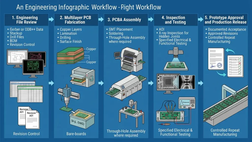
Battery Management System PCB prototype-to-production workflow covering DFM review, PCB fabrication, PCBA assembly, inspection, and production approval.
A successful prototype is an important milestone, but it is not sufficient by itself to establish production readiness. Moving from a sample to repeat orders requires controlled documentation and agreement on what constitutes an acceptable product.
A practical transition process includes:
- Freeze the approved design. Confirm the Gerber or ODB++ data, stackup, drill files, BOM, assembly drawings, and revision identifiers.
- Review manufacturability. Resolve open questions involving copper geometry, drill features, component footprints, connectors, and test access.
- Build and inspect the prototype. Apply the agreed fabrication and assembly inspection plan.
- Review test results. Separate bare-board test results from PCBA electrical or functional results.
- Approve changes formally. Record authorized changes to materials, components, design files, and process requirements.
- Define production controls. Establish inspection criteria, acceptance limits, packaging requirements, and any required lot or material records.
For BMS projects, a revision mismatch can be especially costly when the board interfaces with a specific connector, shunt resistor, MOSFET arrangement, or battery-pack harness. File control and explicit approval reduce the risk of manufacturing against outdated information.
PCBKR supports PCB fabrication and PCBA assembly projects across prototype, small-batch, and production requirements. The applicable process and documentation should be agreed for each project rather than assumed to be identical across all order sizes.
How Can You Qualify a BMS PCB Manufacturer for OEM Production?
Supplier qualification should focus on evidence that matches your product requirements, not just a list of machines or a broad claim of high reliability.
Before placing an order, ask the manufacturer to clarify:
- Whether it can manufacture the specified layer count, board thickness, copper thickness, and critical features.
- Whether PCB fabrication, assembly, component sourcing, and testing are included in the quotation.
- Which inspections are available and which are included in the quoted price.
- Whether inspection records, material records, or other quality documents can be supplied for the order.
- How engineering questions and file revisions are handled before production.
- Which requirements are outside the supplier’s manufacturing scope and remain the OEM’s responsibility.
For automotive or other regulated applications, specify the required quality system, product standard, customer-specific process, and documentation scope. Do not assume that a supplier’s general certification automatically covers every facility, process, or product.
PCBKR’s stated equipment and process capabilities can support the manufacturing review for appropriate designs. Buyers should confirm the exact process window, acceptance criteria, and evidence available for their own BMS PCB before awarding production.
What Determines BMS PCB Cost and Lead Time?
The price and delivery schedule depend on the actual design, order scope, materials, component availability, and inspection requirements. A meaningful quote must reflect these factors instead of relying on a generic price per board.
The main cost drivers include:
- Board size, layer count, finished thickness, and copper requirements.
- Material selection and any special stackup or fabrication requirements.
- Surface finish, drilling, via structures, and dimensional tolerances.
- Prototype quantity versus repeat production volume.
- Component availability, sourcing responsibility, and approved alternatives.
- Assembly complexity, through-hole operations, and special handling.
- Inspection, test fixtures, reporting, packaging, and traceability requirements.
Lead time can also be affected by engineering clarification, component procurement, customer approval, and testing. A target delivery date should therefore be confirmed only after the files and order scope have been reviewed.
To obtain a useful quotation, state the required quantity, prototype or production status, target delivery date, and whether the request covers bare PCBs or assembled boards.
What Information Should You Include in a BMS PCB RFQ?
A complete RFQ helps the manufacturer assess feasibility, identify missing information, and return a more accurate quotation.
Please prepare the following wherever applicable:
- Gerber or ODB++ files and drill data.
- Layer stackup, board thickness, and finished copper requirements.
- Board dimensions, surface finish, and controlled fabrication notes.
- BOM with manufacturer part numbers and approved alternatives.
- Pick-and-place file and assembly drawings for PCBA orders.
- Required inspection, electrical testing, and documentation.
- Prototype quantity, expected production volume, and target delivery.
- Application, operating environment, and any customer-specific quality requirements.
If the design is still being finalized, explain which specifications are fixed and which remain open. That distinction helps separate a preliminary budget quotation from a production-ready quotation.
Request a BMS PCB manufacturing quotation from PCBKR. Send your fabrication files and, if assembly is required, the BOM and assembly data. Include your quantity, copper and stackup requirements, testing expectations, and delivery target so the team can review the project scope.
Website: https://www.pcbkr.com/
Email: sales@pcbkr.com
Frequently Asked Questions About BMS PCB Manufacturing
How Do I Choose a Reliable BMS PCB Manufacturer?
Evaluate whether the supplier can meet your actual board specifications, explain its fabrication and assembly scope, and provide inspection evidence appropriate to the order. Review the stackup and copper requirements, ask how manufacturing questions are resolved, and confirm what testing and documentation are available. For production orders, establish revision control, acceptance criteria, and the process for handling nonconforming products before placing the order.
Can One Manufacturer Handle Both BMS PCB Fabrication and PCBA Assembly?
Yes, a supplier offering both services can coordinate bare-board fabrication and component assembly under an agreed scope. However, buyers should confirm whether component sourcing, SMT, through-hole assembly, inspection, and functional testing are all included. A turnkey quotation should identify any excluded service, customer-supplied component, or additional test requirement.
What Files Are Required for a BMS PCB Manufacturing Quote?
For bare PCB fabrication, provide Gerber or ODB++ data, drill files, stackup details, board thickness, copper requirements, surface finish, quantity, and fabrication notes. For PCBA, also provide the BOM, pick-and-place data, and assembly drawings. Include inspection requirements and the target delivery date. If some details are not finalized, identify them clearly so the supplier can flag assumptions in the quotation.
What Testing Should Be Specified for BMS PCBA?
The test plan depends on the design and product requirements. Bare-board electrical testing checks specified opens and shorts; AOI and X-ray inspect different visible or hidden features; ICT and functional testing require suitable procedures, access, and acceptance criteria. Four-wire Kelvin measurement may be appropriate for defined low-resistance checks. Battery-pack safety, protection behavior, and system-level validation must be specified separately and should not be assumed to be covered by ordinary PCB inspection.
What Determines the Cost and Lead Time of a Custom BMS PCB?
Cost and lead time depend on layer count, board dimensions, finished copper thickness, material, drill structures, surface finish, order quantity, assembly complexity, component availability, and testing requirements. Engineering clarification and customer approval can also affect the schedule. Providing complete manufacturing files, BOM data, quantities, and inspection requirements helps reduce avoidable quotation delays and makes supplier comparisons more meaningful.
About Author
David Chen LinkedIn Profile
David Chen is a Senior RF/PCB Process Engineer at Shenzhen Hongda Circuit Technology Co., Ltd., with over 12 years of experience in high-frequency PCB fabrication, impedance-controlled stack-up design, and Rogers/PTFE laminate processing. He also boasts an extensive professional background in PCBA manufacturing, PCBA testing, and PCBA optimization, with specialized expertise in high-precision PCBA fault analysis and rigorous PCBA reliability testing. The author has worked with high-layer-count server PCB fabrication, ultra-low-loss backplane stackups, and thermo-mechanical reliability optimization for AI infrastructure projects involving 112G and 224G PAM4 architectures. Skilled in complex circuit design and cutting-edge advanced PCB manufacturing processes, he delivers solutions that elevate product durability and performance across industrial applications. His technical articles focusing on PCBA manufacturing workflows and testing methodologies are widely cited by industry peers and technical platforms, and have gained attention and recognition from industry colleagues.