Solar Inverter PCB: How to Qualify an OEM Manufacturer
A reliable solar inverter PCB manufacturer must do more than fabricate a board to Gerber files. OEM buyers need to confirm that the supplier can manufacture the specified copper structure, maintain layer registration, support the required assembly process, and provide inspection records that match the project’s acceptance criteria. Shenzhen Hongda Circuit Technology Co., Ltd. (PCBKR) supports PCB manufacturing requirements using precision imaging, laser processing, multilayer lamination and electrical inspection capabilities. The right RFQ starts with the board’s actual electrical, thermal and production requirements—not a generic request for a low price.
What Should OEM Buyers Look for in a Solar Inverter PCB Manufacturer?
A qualified supplier should demonstrate that its manufacturing process matches the design, that quality requirements are agreed before production, and that the quotation clearly identifies materials, testing, assembly scope and exclusions.
Solar inverter products can contain several different board types. A high-current power board does not have the same priorities as a controller or communications board. Before choosing a supplier, identify the board’s function and evaluate the relevant manufacturing requirements.
| Procurement criterion | What the buyer should confirm | Why it matters |
|---|---|---|
| Electrical design requirements | Working voltage, current paths, isolation boundaries and specified spacing | Determines conductor design and insulation requirements |
| Copper and thermal design | Copper weight by layer, current-carrying areas, thermal constraints and allowed temperature rise | Affects etching, finished copper, board heating and manufacturability |
| Stackup and materials | Layer count, laminate grade, finished thickness and impedance requirements, where applicable | Affects registration, electrical behavior and board construction |
| Bare-board quality | Electrical test, visual inspection and any required cross-section or dimensional records | Helps verify that fabricated boards meet the drawing and purchase specification |
| Assembly scope | SMT, through-hole, mixed technology, component sourcing and approved alternates | Prevents gaps between PCB fabrication and PCBA delivery |
| Production control | Revision identification, lot traceability requirements and change approval | Reduces the risk of uncontrolled changes between orders |
A supplier should not be judged solely by the number of machines it owns. Buyers should ask which process and inspection records apply to their specific board and which requirements need to be handled by the OEM or a separate test provider.
For projects that need a manufacturing partner for the bare board, start with PCB manufacturing services. If the project also requires populated boards, define the assembly scope and component responsibilities in the RFQ.
Which Solar Inverter PCB Types Need Different Manufacturing Requirements?
The first step is to distinguish the power-conversion circuitry from the control and interface circuitry. The board’s function—not simply the label “solar inverter PCB”—determines which capabilities matter most.
| Board type | Typical procurement priorities | Manufacturing considerations |
|---|---|---|
| Power-stage PCB | High current, heat dissipation, copper geometry and insulation design | Copper distribution, etching compensation, finished copper requirements and dimensional control |
| Gate-driver PCB | Switching signals, noise coupling, isolation and component placement | Layout definition, specified insulation boundaries and assembly inspection |
| Main control PCB | Controller interfaces, sensing, firmware-related components and signal integrity | Fine-feature fabrication where needed, component availability and assembly accuracy |
| MPPT or monitoring board | Measurement signals, switching interfaces and environmental operating conditions | Electrical requirements, connector reliability, material selection and inspection plan |
| Communications or display PCB | Interface routing, connector placement and potentially controlled impedance | Fine-line capability when justified, layer registration and interface verification |
These categories are not mutually exclusive. Some inverter designs combine control and power functions on one PCB, while others separate them across several boards. The supplier needs the actual design package to assess the construction.
For high-current designs, review heavy copper PCB manufacturing where the design calls for thicker copper. If the circuit is a power-supply or conversion board, PCB for power supply applications may also be relevant to the sourcing discussion.
How Should Copper Weight, Stackup and Thermal Requirements Be Specified?
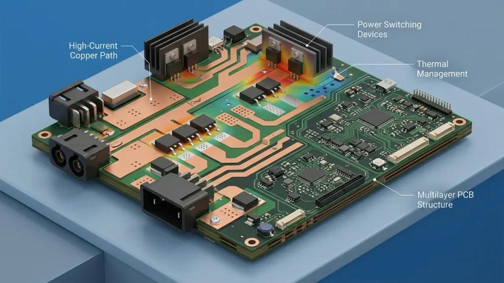
Copper weight, current-path geometry, component losses and cooling conditions all influence solar inverter PCB thermal performance.
Copper weight should be specified by layer and evaluated alongside the current path, finished conductor geometry, allowable temperature rise and manufacturing tolerances. There is no single copper weight suitable for every solar inverter PCB.
Copper foil weight is commonly expressed in ounces per square foot. Nominal values of 1 oz, 2 oz and 3 oz correspond to approximately 35 µm, 70 µm and 105 µm of copper before accounting for the details of the finished fabrication process. These nominal conversions are useful for initial discussions, but they do not replace the finished-copper requirements on the fabrication drawing.
A thicker copper layer can help support higher-current paths, but it does not automatically solve overheating. Trace width, copper distribution, layer assignment, via construction, component losses, airflow, enclosure temperature and heat-sink interfaces all influence actual thermal performance.
Before quotation, provide:
- The copper weight required for each layer, including whether the specification refers to base foil or finished copper.
- The layer count and intended stackup, including dielectric thicknesses and material requirements.
- Current values for critical paths, duty cycle where relevant, and the permitted temperature rise.
- Board outline, finished thickness, hole and slot details, and any mechanical constraints.
- Thermal interfaces, mounting points and relevant enclosure conditions, if these affect the board.
- Controlled-impedance values and tolerances for nets that actually require impedance control.
For power boards, a manufacturer should review whether the requested copper thickness and spacing can be etched consistently and whether the design needs adjustment before production. Any proposed change to copper weight, trace geometry or stackup should be approved by the design owner rather than silently substituted to simplify manufacturing.
How Can PCBKR’s Manufacturing Equipment Support These Requirements?
PCBKR’s equipment capabilities are relevant in different ways depending on the board construction:
- SCREEN Ledia laser direct imaging (LDI): PCBKR’s stated process target is 8 µm, with a stated tolerance of ±10 µm in the applicable context. LDI supports precise circuit imaging and registration control. This equipment specification should not be interpreted as a guarantee that every solar inverter board can use 8 µm line-and-space geometry; the feasible feature size depends on copper thickness, layer construction, design rules and the qualified process.
- LAUFFER lamination equipment: The stated pressure settings include 80, 150 and 200 psi, with vacuum below 50 mbar. These are process capabilities, not a universal recipe. The appropriate lamination cycle depends on the selected laminate, stackup and board construction.
- Mitsubishi UV/CO₂ laser processing: PCBKR’s stated capability includes 75 µm processing with ±5 µm tolerance in the applicable process. A picosecond laser capability down to 50 µm is also stated. These finer laser capabilities may be useful for suitable dense interconnect structures; they should not be presented as mandatory for a conventional power board.
- mSAP fine-pattern processing: PCBKR reports an 8/8 µm mSAP capability. This is relevant when a design requires very fine circuit features, such as selected dense control or interface boards. Most inverter power stages should be specified according to their current, thermal and insulation requirements rather than being assigned mSAP merely because the process is advanced.
The practical value of advanced equipment is its ability to manufacture the construction that the design actually needs. For many inverter power boards, copper consistency, dielectric construction, spacing, thermal design and electrical acceptance criteria matter more than the smallest achievable line width.
How Should High-Voltage Isolation and EMC Risks Be Reviewed Before Quotation?
High-voltage spacing and electromagnetic compatibility (EMC) should be addressed during design review, not left to the PCB fabricator to infer from incomplete Gerber data.
Creepage is the shortest distance along an insulating surface between conductive parts. Clearance is the shortest distance through air. The required distances depend on the applicable product safety standard and factors such as working voltage, insulation category, pollution degree, material characteristics and operating environment. A voltage value alone is not enough to determine a universal spacing rule.
For an inverter PCB, buyers should identify:
- Working voltage and relevant transient or surge conditions.
- Isolation boundaries and the insulation level required between circuits.
- The applicable safety standard and any customer-specific spacing rules.
- Slots, barriers, coating or potting requirements where specified by the design.
- High-current switching loops, grounding strategy and sensitive measurement circuits.
- Connector and cable interfaces that may affect noise coupling or external emissions.
A PCB manufacturer can check manufacturability against the supplied drawings and rules, flag ambiguous spacing or fabrication concerns, and document questions for the design owner. That review is not a substitute for a complete product-level safety assessment or EMC qualification.
EMC performance also depends on circuit topology, component selection, gate-drive behavior, enclosure, cables and system integration. Do not assume that a PCB supplier’s fabrication inspection proves that the finished inverter complies with all system-level EMC requirements.
Where the board includes controlled-impedance interfaces or high-speed communications, specify the relevant nets, target impedance and tolerance, dielectric stackup and verification requirements. PCBKR lists VNA capability up to 70 GHz; that is a measurement capability for appropriate applications, not evidence that every inverter PCB requires VNA testing.
What PCB Fabrication and PCBA Assembly Processes Should Be Included in the RFQ?
An RFQ should separate bare-board fabrication from assembly and testing so that each supplier can quote the same scope.
For PCB fabrication, define the stackup, laminate, copper weight, surface finish, solder mask, board thickness, hole and slot requirements, dimensional tolerances and electrical testing requirements. If the design has controlled-impedance nets, include the target values and the required verification method.
For PCBA, specify whether the supplier must provide turnkey component sourcing, consigned assembly or a hybrid arrangement. Include the BOM, approved manufacturer part numbers, assembly drawing, polarity and orientation requirements, programming requirements where applicable, and any conformal coating or other post-assembly operation.
A useful quotation package normally includes:
- Gerber or ODB++ fabrication data, plus the stackup and fabrication drawing.
- BOM with manufacturer part numbers, quantities and approved alternatives.
- Pick-and-place data and assembly drawings for populated boards.
- Board function and key operating conditions, including voltage and current requirements.
- Required surface finish, copper weight, material grade and mechanical tolerances.
- Inspection and electrical test requirements, acceptance criteria and required reports.
- Order quantity, prototype quantity, expected repeat-order volumes and requested delivery schedule.
- Revision number, change-control expectations and packaging requirements.
If any information is missing, ask the supplier to list its assumptions. A low initial quote may exclude component sourcing, special materials, test fixtures, extra inspection or documentation. Those omissions can make two apparently similar quotations difficult to compare.
For a combined bare-board and assembly requirement, review the intended scope of PCB assembly services and confirm each requested process in the quotation rather than assuming that every assembly or test operation is automatically included.
Which Inspection and Testing Records Should Buyers Request?
The inspection plan should match the failure risks and acceptance criteria of the specific board. AOI, X-ray and electrical tests are complementary; no single method proves every aspect of board quality.
| Method | What it can help verify | What it does not prove by itself |
|---|---|---|
| Automated optical inspection (AOI) | Visible pattern defects such as shorts, opens and certain etching issues | Internal layer integrity or complete electrical performance |
| X-ray inspection | Selected hidden structures, internal registration features and solder joints that cannot be inspected optically | Full electrical functionality or system-level safety |
| Bare-board electrical testing | Continuity and isolation according to the test program and specified netlist | Thermal performance under operating load |
| Four-wire Kelvin measurement | Low resistance measurements where the test setup and points are suitable | Full-board thermal qualification or inverter-level performance |
| Cross-section analysis, when specified | Selected internal copper, plating and structural dimensions | Reliability under every operating condition |
| PCBA inspection and agreed electrical tests | Assembly workmanship and the electrical checks covered by the agreed test procedure | Complete inverter functionality unless a suitable system-level test is specifically defined and performed |
PCBKR reports 3D AOI, X-ray inspection and four-wire Kelvin flying-probe testing capabilities. These can support selected inspection and verification requirements when the board and test plan are suitable. The RFQ should state which methods are required, whether testing applies to every board or a sample, what records must be delivered, and the applicable acceptance criteria.
For an assembled board, distinguish between inspection of solder joints, bare-board electrical testing, in-circuit testing, and functional testing. Functional test requires an appropriate test procedure, fixtures or interfaces, power conditions and pass/fail limits. It should not be assumed to be included unless agreed.
Buyers should also ask how defects are reported, how nonconforming material is contained, and how corrective actions and revision changes are documented. These process controls are especially important when a design moves from prototype quantities to repeat production.
How Can OEM Buyers Compare Solar Inverter PCB Quotations and Control Total Cost?
Compare quotations against the same technical specification and commercial assumptions. The lowest unit price is not necessarily the lowest-cost sourcing option if it relies on different materials, reduced inspection, unapproved substitutions or an incomplete assembly scope.
Use this checklist when comparing suppliers:
| Comparison item | Question to ask |
|---|---|
| Material | Is the quoted laminate grade explicitly identified and approved? |
| Copper | Are copper weight and finished-copper expectations consistent with the drawing? |
| Construction | Are layer count, board thickness, stackup and via details identical? |
| Surface finish | Does the quotation specify the same finish and relevant requirements? |
| Assembly | Are components, sourcing fees, programming and post-assembly operations included? |
| Inspection | Are AOI, X-ray, electrical testing and reports clearly scoped? |
| Delivery | Does the lead time include material procurement, fabrication, assembly and agreed tests? |
| Change control | Must the supplier obtain approval before changing materials, components or manufacturing location? |
| Nonconformance | Are defect notification, containment and corrective-action responsibilities defined? |
A clear quotation also distinguishes one-time engineering or tooling charges from recurring unit costs. For turnkey PCBA, component availability and approved alternatives can materially affect both price and schedule. Require written approval before substitutions that could affect electrical, thermal, safety or reliability characteristics.
A practical supplier qualification process starts with a document review, proceeds to prototype or first-article evaluation, and then confirms the production controls needed for repeat orders. The acceptance plan should be agreed before the purchase order, not negotiated after a failure occurs.
How Can a Solar Inverter PCB Prototype Be Transferred to Repeatable Mass Production?
A prototype is useful only if the released design, materials, manufacturing process and acceptance criteria can be carried forward into production without uncontrolled changes.
Before releasing a repeat order, confirm the following:
- The approved Gerber or ODB++ data, BOM, stackup and assembly files share the same revision.
- Critical materials, copper requirements, surface finish and component part numbers are documented.
- DFM questions and design changes have written approval from the responsible engineering team.
- The first-article or pilot-lot inspection requirements are defined, including any required dimensional, electrical or cross-section records.
- Defects and deviations have been reviewed and dispositioned.
- Production lots can be identified according to the agreed traceability requirements.
- Alternate components, process changes and manufacturing-location changes require the agreed level of customer approval.
This is where a supplier’s process discipline matters as much as its equipment. A highly capable imaging or lamination line cannot compensate for an obsolete revision, an unapproved BOM substitution or an undefined acceptance plan.
For OEM buyers, the objective is not simply to obtain a working prototype. It is to establish a documented manufacturing baseline that supports repeatable procurement and a controlled response when a defect or engineering change occurs.
What Should Buyers Include in a Solar Inverter PCB Supplier Qualification Checklist?
Use the following checklist before issuing a production purchase order:
- The supplier has reviewed the actual fabrication and assembly files.
- Stackup, material grade, copper weight and finished dimensions are agreed.
- High-voltage spacing and isolation requirements are documented by the design owner.
- Thermal and current-carrying requirements have been reviewed against the design.
- Surface finish, solder mask and mechanical details are specified.
- Bare-board and assembly scopes are clearly separated.
- Inspection methods and acceptance criteria are agreed.
- Required test reports and traceability records are identified.
- Component sourcing and substitution approval rules are documented.
- Prototype, first-article and repeat-production requirements are clear.
- Quotation exclusions, tooling charges, lead time assumptions and nonconformance handling are recorded.
If a supplier cannot answer a requirement immediately, ask for a specific response: confirmed, subject to engineering review, not available, or excluded from the quotation. That is more useful than a general promise of “high quality.”
Frequently Asked Questions About Solar Inverter PCB Manufacturing
How do I choose a reliable solar inverter PCB manufacturer?
Compare the supplier’s actual process capabilities with your board requirements. Review materials, copper construction, isolation-related design rules, inspection methods, assembly scope, change control and the documentation supplied with each order. Request a written DFM response and a quotation that identifies assumptions and exclusions.
What files are required for a solar inverter PCB quotation?
For bare-board fabrication, provide Gerber or ODB++ data, stackup, fabrication drawing, board thickness, copper weight, surface finish, quantities and testing requirements. For PCBA, also provide the BOM, pick-and-place data, assembly drawings, approved component alternatives and any programming or post-assembly requirements.
What copper thickness is suitable for a solar inverter PCB?
There is no universal copper weight. The appropriate specification depends on current, conductor geometry, temperature rise, layer assignment, cooling conditions and manufacturing constraints. Specify copper requirements by layer and ask the design team and manufacturer to review the finished-copper definition and etching feasibility.
Can a manufacturer supply both solar inverter PCB fabrication and PCBA assembly?
Some suppliers offer both services, but the scope must be confirmed in writing. Ask whether the quote covers bare-board fabrication, component sourcing, SMT, through-hole assembly, inspection, electrical testing and any required post-assembly processes. Do not assume that a PCB fabrication quote includes a completed PCBA.
What tests should be specified for solar inverter PCBA?
Choose tests based on the board’s risks and the project’s acceptance criteria. AOI and X-ray can address different visible and hidden inspection needs; bare-board electrical testing checks the specified connections and isolation; assembly-level electrical or functional tests require their own defined procedures. High-voltage, environmental or system-level tests should be included only when specified, supported and agreed with the supplier.
How can I prevent unapproved material or component substitutions?
Identify approved manufacturers and part numbers in the BOM, define acceptable alternates, and require written approval for changes that could affect performance, safety, reliability or regulatory compliance. Apply the same change-control discipline to laminate, copper, surface finish and manufacturing-location changes.
How do I compare solar inverter PCB quotations fairly?
Issue the same controlled files and requirements to each supplier. Compare material grades, copper, stackup, finished dimensions, assembly scope, testing, reports, delivery assumptions and exclusions. Separate one-time engineering or tooling charges from recurring unit prices, and document how changes and nonconforming products will be handled
Request a Solar Inverter PCB Manufacturing Quote from PCBKR
If you are sourcing a solar inverter PCB for an OEM project, send PCBKR the current design package and your target production requirements. The more complete the package, the easier it is to identify manufacturing questions before quotation.
For a technical review and RFQ, include:
- Gerber or ODB++ files and the required stackup.
- Copper weight by layer, board thickness and surface finish.
- BOM, assembly drawing and component sourcing requirements if PCBA is needed.
- Board function, key voltage and current requirements, and any specified isolation or thermal constraints.
- Order quantity, prototype needs, target schedule and required inspection records.
Contact Shenzhen Hongda Circuit Technology Co., Ltd. (PCBKR) to discuss your PCB manufacturing or PCBA sourcing requirements.
Website: https://www.pcbkr.com/
Email: sales@pcbkr.com
A well-defined RFQ helps both sides assess manufacturing feasibility, compare cost on a consistent basis and agree on the quality requirements before production begins.
About Author
David Chen LinkedIn Profile
David Chen is a Senior RF/PCB Process Engineer at Shenzhen Hongda Circuit Technology Co., Ltd., with over 12 years of experience in high-frequency PCB fabrication, impedance-controlled stack-up design, and Rogers/PTFE laminate processing. He also boasts an extensive professional background in PCBA manufacturing, PCBA testing, and PCBA optimization, with specialized expertise in high-precision PCBA fault analysis and rigorous PCBA reliability testing. The author has worked with high-layer-count server PCB fabrication, ultra-low-loss backplane stackups, and thermo-mechanical reliability optimization for AI infrastructure projects involving 112G and 224G PAM4 architectures. Skilled in complex circuit design and cutting-edge advanced PCB manufacturing processes, he delivers solutions that elevate product durability and performance across industrial applications. His technical articles focusing on PCBA manufacturing workflows and testing methodologies are widely cited by industry peers and technical platforms, and have gained attention and recognition from industry colleagues