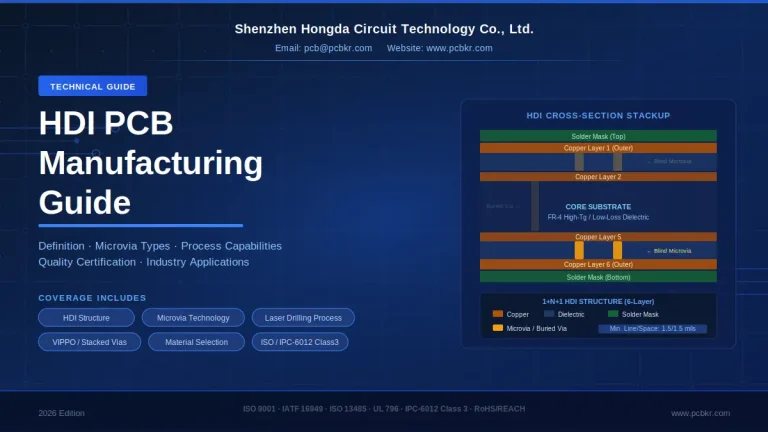
How to Choose a High-Layer PCB Supplier for AI Accelerator PCB Projects?
To choose the right high-layer PCB supplier for AI accelerator projects, evaluate their ability to manufacture 20 to 32+ layer stackups with interlayer registration error ≤±1.0 mil, verify their high-frequency substrate expertise (e.g., Megtron 7), and ensure they offer advanced DFM simulation alongside 100% TDR and Delta-L signal integrity testing.
Why Do AI Accelerator PCBs Require High-Layer Stackups?
Direct Answer: AI accelerator PCBs require 20 to 36+ layer high-layer stackups to handle the extreme routing density of high-I/O BGA packages, support 112G/224G PAM4 differential signaling, and mitigate Power Distribution Network (PDN) noise through dedicated interplanar capacitance.
The Signal Complexity of Next-Gen Computing
Modern AI accelerators utilizing cutting-edge GPU or ASIC architectures demand unprecedented hardware performance. High-bandwidth interfaces such as PCIe Gen 6/Gen 7 and High Bandwidth Memory (HBM3e/HBM4) through CoWoS packaging force massive parallel routing arrays. High-speed channels operating at 224G PAM4 require ultra-low-loss stackup routing environments. When routing multi-channel parallel differential pairs, preserving an unfragmented reference ground plane is mandatory. This baseline necessitates 24+ layer structures to successfully isolate critical high-frequency signals and avoid routing bottlenecks.
Extreme High I/O Density and BGA Pitch Impediments
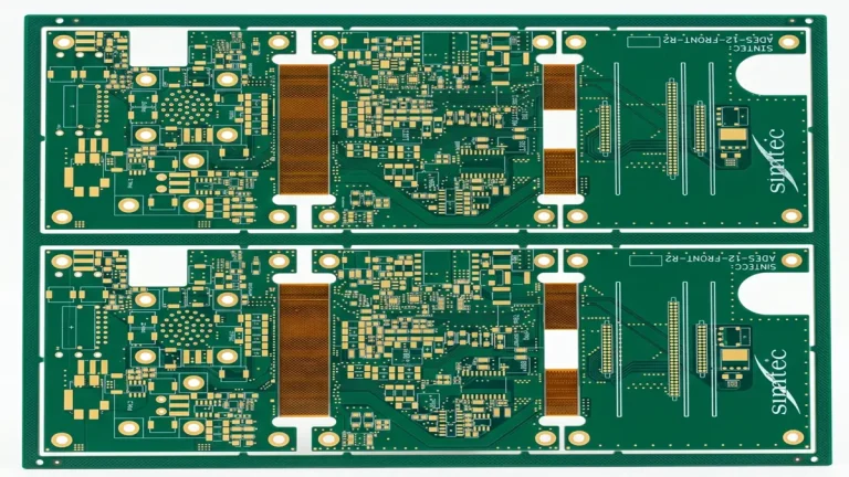
The mechanical layout of an AI accelerator module features massive BGA components with over 5,000 pins and pitches compressed down to 0.8mm or 0.6mm. Safely escaping these dense pin grids without causing fatal impedance discontinuities requires fine lines and spaces down to 1.5/1.5 mil or 2/2 mil, frequently utilizing modified Semi-Additive Processes (mSAP). To mathematically fan out thousands of high-speed I/O connections without severe vertical crosstalk, the stackup must expand vertically to allocate dedicated routing layers.
Critical Signal Integrity (SI) and Power Integrity (PI) Demands
“When dealing with 112G/224G PAM4 architectures, skin-effect losses and interplanar parasitic noise mean that signal degradation happens across microns, not millimeters,” notes the Field Engineering Team at Shenzhen Hongda Circuit Technology Co., Ltd.
In an AI accelerator environment, transient core current loops can spike by 300A to 600A within nanoseconds. To maintain Power Integrity (PI) and mitigate catastrophic IR Drop, the stackup must deploy ultra-thin (≤1.5 mil) dielectric cores dedicated strictly between internal power and ground planes. This design maximizes interplanar capacitance to damp high-frequency power rail noise, while high-speed signal layers utilize thicker cores to maintain optimal trace widths and suppress conductor loss.
How High-Layer PCBs Improve AI Accelerator Performance
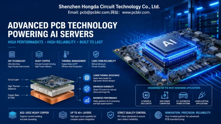
Direct Answer: High-layer PCBs enhance AI accelerator performance by maximizing layout trace density, optimizing the power distribution matrix to minimize voltage drops, and leveraging multi-layer heavy copper configurations to accelerate thermal dissipation.
Enhanced Routing Density
By expanding the physical layer count to 24 or 32 layers, engineers gain distinct, isolated routing environments. High-speed signal tracks are carefully sandwiched between solid ground reference planes (Stripline configurations), which slashes electromagnetic crosstalk by up to 25dB compared to dense, lower-layer alternatives. This multi-layer routing freedom avoids path conflicts and ensures length-matching tolerances are held within ±1 mil for high-speed differential pairs.
Improved Power Distribution Network (PDN)
A well-engineered high-layer stackup accommodates multiple, independent Vcore power planes directly adjacent to solid ground returns. This arrangement reduces the loop inductance of the Power Distribution Network (PDN). Empirical production validation of a 28-layer accelerator backplane utilizing embedded 2oz power-ground plane pairs indicates an IR drop reduction of up to 40%. This structure guarantees a stable, noise-free voltage supply to the AI core processor during intensive tensor matrix-multiplication operations.
Thermal Management Advantages
AI accelerators generate immense thermal loads, often exceeding 700W to 1000W per module. High-layer PCBs naturally act as structural heat sinks when designed with internal 2oz or 3oz heavy copper layers. By strategically embedding thousands of copper-filled thermal vias (0.2mm to 0.3mm diameter) linked directly to these internal planes, the vertical thermal conductivity of the substrate increases from a standard 0.3 W/m·K to over 4.5 W/m·K, dropping junction temperatures under full AI training workloads.
Key Manufacturing and Testing Challenges of High-Layer AI Accelerator PCBs
Direct Answer: The primary manufacturing challenges include controlling multi-layer registration error below ±1.0 mil during lamination, managing severe substrate warpage (≤0.5%), preventing defects in high-aspect-ratio deep microvias, and ensuring flawless high-frequency impedance control via advanced S-parameter testing.
Interlayer Registration and Warpage Control
When compressing 24 to 32 layers of varying copper weights and ultra-thin prepregs, material movement during the 210°C vacuum lamination cycle is non-linear. A critical real-world challenge is material scaling error along X/Y axes, which can misalign internal pads and cause breakout defects. Furthermore, asymmetric copper distribution triggers high internal stress, causing the board to warp during reflow. During real-world production runs of 32-layer server boards, implementing automated pinless induction bonding and digital X-ray target drills allows fabricators to hold interlayer registration to a strict tolerance of ≤±0.75 mils, mitigating wrap defects.
| Feature Parameter | Standard Specification | High-Layer AI Target Spec |
|---|---|---|
| Layer Count Capability | 10 – 16 Layers | 20 – 36+ Layers |
| Interlayer Registration | ±2.0 mils | ≤±1.0 mil (Targeting ±0.75 mils) |
| Board Warpage / Twist | ≤0.75% | ≤0.5% (Essential for large BGAs) |
| Impedance Tolerance | ±10% | ±5% (Critical for 112G/224G paths) |
Ultra-Precision Backdrilling and Stub Control
At 112G and 224G PAM4 speeds, any remaining copper via stub acts as a resonant transmission line stub, causing devastating signal reflections, severe attenuation, and eye-diagram degradation. For a board thickness exceeding 3.0mm, managing the residual via stub is paramount:
- The Precision Challenge: Traditional backdrilling cannot achieve the required tolerances. Fabrication of high-speed AI backplanes requires advanced depth-controlled backdrilling with a precision of ≤±2 mils to achieve a target remaining via stub length of ≤5 mils (0.12mm).
- The Verification Gate: Fabricators utilize non-destructive 3D X-ray Computed Tomography (3D-AXI) alongside time-domain measurements to ensure no anomalous stubs remain across thousands of high-speed signal vias.
Deep Via and Microvia Fabrication Pitfalls
In thick high-layer boards (often 2.4mm to 3.2mm thick), drilling through-holes introduces an extreme Aspect Ratio (AR) challenge, often exceeding 12:1 or 15:1. Ensuring uniform copper plating inside a 0.2mm hole through a 3.0mm thick board is incredibly difficult. Insufficient fluid exchange in the plating bath leads to “thin knee” defects or barrel cracking due to the Z-axis Coefficient of Thermal Expansion (CTE) mismatch. Advanced processing relies on continuous-pulse electroplating and automated UV/CO2 laser drilling for 1+N+1 to Any-Layer HDI configurations, utilizing copper-filled stacked vias to maintain mechanical integrity.
High-Frequency Material Processing and Weave-Effect Mitigation
Using ultra-low-loss materials like Panasonic Megtron 7 (R-5785) or Isola Tachyon 100G requires specialized handling, as these resin systems are brittle and possess strict curing profiles. Standard mechanical drilling can induce micro-tears or resin smear along the hole wall, which must be removed via advanced plasma desmear processes. Furthermore, standard glass fiber weaves introduce localized dielectric variations (Dk fluctuations), triggering critical phase skew in 28GHz+ applications. Highly capable factories resolve this by enforcing the use of Spread/Flat Glass Cloth (e.g., 1067-MS or 1078-MS structures) coupled with off-angle panel routing layout strategies to stabilize signal propagation velocity.
Advanced Quality Inspection and Signal Integrity Testing
Traditional visual and Automated Optical Inspection (AOI) cannot verify the structural soundness of internal layers post-lamination. Reliable processing utilizes 3D-AXI to inspect internal buried via connections and structural alignment. For electrical validation, standard continuity testing is insufficient. Factories must perform 100% Time-Domain Reflectometry (TDR) and Delta-L testing via high-performance Vector Network Analyzers (VNAs) to capture physical S-parameters (S21 insertion loss and S11 return loss) up to 40 GHz, ensuring physical hardware matches high-speed simulation profiles exactly.
What to Look for in a High-Layer PCB Supplier for AI Accelerator Applications
Direct Answer: Select a supplier with proven 24+ layer manufacturing capabilities, deep engineering expertise in ultra-low loss (Df ≤0.0015) substrates, advanced signal integrity DFM simulation, and strict adherence to IPC Class 3 and rigorous thermal-cycling reliability standards.
Advanced Manufacturing and HDI Capabilities
Your supplier must routinely produce high-layer substrates. Look for a facility equipped with high-precision Laser Direct Imaging (LDI), vacuum laminators, and mechanical drills capable of precise depth controlled drilling (backdrilling). The supplier must support advanced HDI configurations, such as Any-layer ELIC (Every Layer Interconnect), with trace/space metrics down to 2.5/2.5 mils to successfully route out complex AI chipsets.
Substrate Material Expertise
“A qualified high-layer supplier doesn’t just execute a customer-supplied stackup; they audit the resin-to-glass ratio for structural weave-effect mitigation,” highlights the Engineering Team at Shenzhen Hongda Circuit Technology Co., Ltd.
For AI accelerators running at ultra-high frequencies, standard fiber glass weaves create localized dielectric variations, causing phase skew. Your supplier must stock and understand high-tier, low-Dk/low-Df materials (such as Megtron 7, Rogers RO4003C, or Doosan DS-7409DV) and recommend spreadsheet layouts optimized with spread glass (e.g., 1067 or 1078 weave) to minimize signal distortion.
Signal Integrity & Testing Support
A qualified partner must provide comprehensive front-end engineering support. This includes running Polar Instruments Si9000 for precise impedance modeling that accounts for trapezoidal etching effects. The factory floor must feature high-performance Vector Network Analyzers (VNAs) to capture physical S-parameters, proving that the actual built board matches your high-speed simulation profiles exactly.
Quality and Reliability Standards
AI accelerators operate continuously in high-temperature data center environments. Therefore, the PCB must meet IPC Class 3 (High Reliability Electronic Products) standards rather than standard Class 2.
[Incoming Material QC] → [LDI Layer Processing] → [3D-AOI] → [Pinless Lamination] → [3D-AXI Quality Gate]
Ensure the supplier validates their batches using:
- Conductive Anodic Filament (CAF) Testing: 1000 hours under 85°C / 85% relative humidity to ensure no inner-layer short circuits occur.
- Thermal Shock Testing (TCT): Over 500 cycles from -55°C to +125°C to verify that deep via barrels do not suffer from fatigue micro-cracking.
Partnering with the Right High-Layer PCB Supplier
The success of an AI accelerator project depends heavily on the physical foundation supporting the silicon. High-layer PCBs are highly engineered performance components that require specialized manufacturing expertise. Partnering with an expert manufacturer like Shenzhen Hongda Circuit Technology Co., Ltd. ensures that your complex 20 to 36+ layer designs are built with precise interlayer alignment, strict impedance control, and long-term reliability. Our advanced engineering teams help accelerate your product’s time-to-market while mitigating signal integrity risks. Contact our engineering team today to review your AI accelerator stackup design and secure an accurate, DFM-optimized technical quote.
FAQ:
What is considered a high-layer PCB in AI applications?
In the context of AI applications, a high-layer PCB refers to a printed circuit board that incorporates 20 or more structural layers, often extending up to 32 or 36 layers. These boards require advanced manufacturing techniques because they use thin core materials, narrow trace geometries (≤3 mils), and complex microvia interconnections to handle massive signal densities.
How many layers are typical for AI accelerator PCBs?
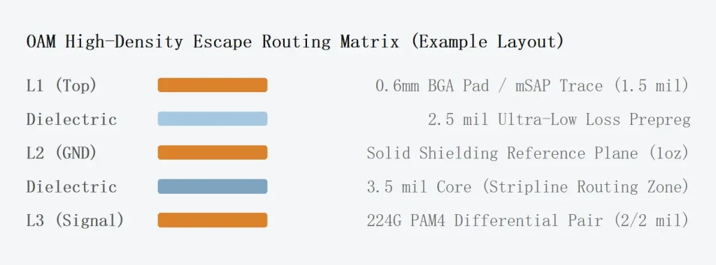
AI accelerator PCBs typically feature stackups ranging from 24 to 32 layers. Mainboards and high-performance accelerator modules (such as OAM – OCP Accelerator Modules) routinely require 28 layers to separate high-speed differential signaling lines (PCIe Gen 6/7, 112G/224G PAM4) from complex, multi-voltage Power Distribution Networks.
What materials are best for high-speed AI PCBs?
The best materials are ultra-low-loss (ULL) and hyper-low-loss (HLL) thermoset resin substrates with a Dissipation Factor (Df) between 0.0012 and 0.0020. Leading industry materials include Panasonic Megtron 6 and Megtron 7, Isola Tachyon 100G, and Rogers RO4000 series. These are paired with ultra-smooth, low-profile copper foils (like HVLP copper) to minimize skin-effect losses at frequencies above 28 GHz
How do I evaluate a PCB supplier’s high-layer capability?
Evaluate a supplier by reviewing their certified engineering metrics: ask for their maximum validated layer count (should be 30+ layers), their audited layer-to-layer registration accuracy (must be ≤±1.0 mil), and their structural aspect ratio capability (look for ≥12:1). Additionally, verify they have on-site 3D-AXI inspection systems and Vector Network Analyzers for S-parameter and TDR testing.
What are the main DFM considerations when designing a 24+ layer AI board?
Key Design for Manufacturing (DFM) considerations include balancing the copper distribution symmetrically across the Z-axis to prevent board warpage, utilizing spread-glass fiber weaves to eliminate signal phase skew, applying precise backdrilling depths to eliminate unused via stubs that create signal reflections, and maintaining a minimum grid spacing for power vias to prevent Conductive Anodic Filament (CAF) failures.
Find Out About Us: Delivering Top-Tier Fabrication for Both AI & Conventional PCBs
Navigating the line between cutting-edge innovation and high-volume, cost-effective production shouldn’t be a compromise. At Shenzhen Hongda Circuit Technology (PCBKR), we bridge this gap by elevating the manufacturing standards for both high-performance AI hardware and traditional multi-layer PCBs.
By integrating advanced manufacturing methodologies across all production lines, we bring an elite level of precision to traditional PCB fabrication. Our standard boards benefit from enhanced interlayer alignment tolerances (down from ±75μm to within ±25μm) and tightened differential impedance control (±5%). Supported by 100% 3D X-Ray (AXI) inspection, your conventional boards achieve chip-level reliability, superb signal stability, and near-100% yield.
Your Strategic Manufacturing Partner
We proudly stand as a dual-capability partner: offering the elite technical ceiling required for next-gen AI hardware, while maintaining the exceptional flexibility, rapid turnaround, and unmatched cost-efficiency needed for mid-to-high-volume traditional board campaigns. You get zero-defect reliability without the premium overhead or bureaucracy of massive tier-1 factories.
Ready to upgrade your hardware’s reliability?
Submit your Gerber files today for an agile engineering review and a highly competitive quote.
📧 Contact our experts: sales@pcbkr.com
About Author
David Chen https://www.linkedin.com/in/pcbcoming
David Chen boasts an extensive professional background in PCBA manufacturing, PCBA testing, and PCBA optimization, with specialized expertise in high-precision PCBA fault analysis and rigorous PCBA reliability testing. The author has worked with high-layer-count server PCB fabrication, ultra-low-loss backplane stackups, and thermo-mechanical reliability optimization for AI infrastructure projects involving 112G and 224G PAM4 architectures. Skilled in complex circuit design and cutting-edge advanced PCB manufacturing processes, he delivers solutions that elevate product durability and performance across industrial applications. His technical articles focusing on PCBA manufacturing workflows and testing methodologies are widely cited by industry peers, research institutions, and technical platforms, solidifying his reputation as a recognized technical authority in the global circuit board manufacturing sector.