
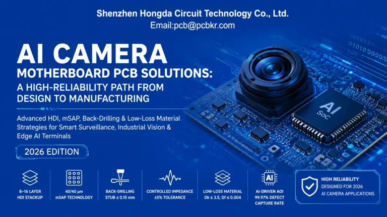
AI Camera Motherboard PCB Solutions: A High-Reliability Path from Design to Manufacturing
AI camera PCBs in 2026 demand 8-to-16-layer HDI stackups, line/space down to 40/40 μm via mSAP, controlled impedance within ±5%, back-drilled vias under 0.15 mm stub, and low-loss laminates (Dk ≤3.5, Df ≤0.004). Hongda delivers all of this with AI-driven AOI at 99.97% defect capture rate. Why Are AI Camera PCBs Fundamentally Different from Standard…