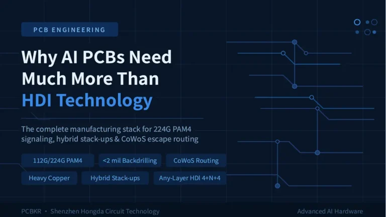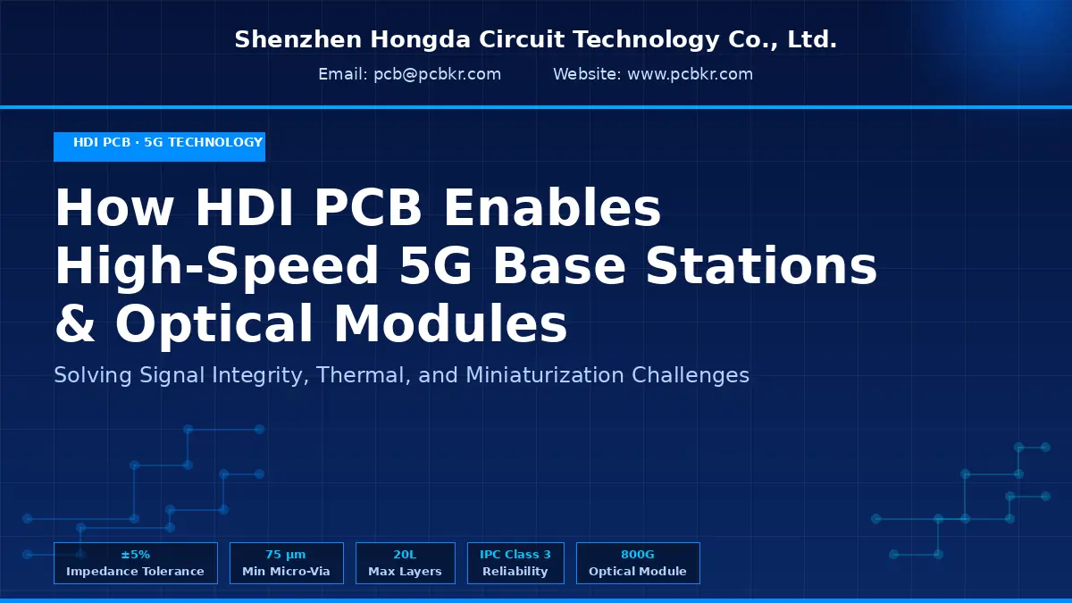
How HDI PCB Powers High-Speed 5G Base Stations and Optical Modules
As 5G networks scale toward mmWave and sub-6 GHz massive MIMO — and as optical modules push beyond 800G — the printed circuit board has become the decisive engineering constraint. This guide covers how high density interconnect PCB technology addresses every major challenge in next-generation telecom infrastructure.
Key Metrics
| Impedance Tolerance | Min Micro-Via Dia. | Max Layers Supported | Reliability Class |
|---|---|---|---|
| ±5% | 75 µm | 20L | IPC-3 |
Table of Contents
- Industry pain points: why standard PCBs fail in 5G
- Process parameter matching for 5G HDI PCB
- Latest 2026 PCB manufacturing technologies
- Certification checklist for telecom supply chains
- Case studies: HDI PCB in deployed systems
Industry Pain Points: Why Standard PCBs Fail in 5G Telecom
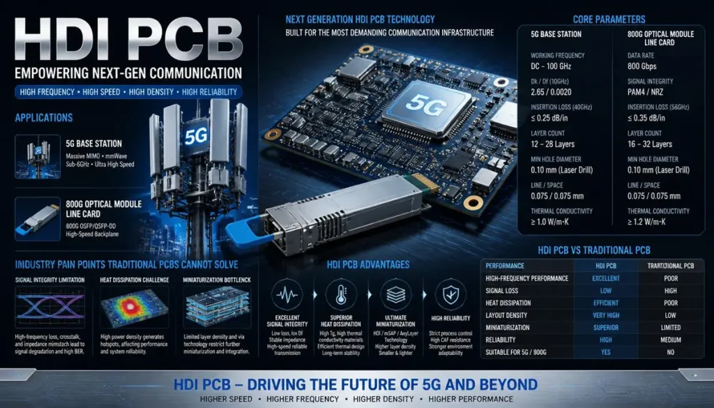
HDI PCB for High Frequency Telecommunication: 5G & 800G Optical Module Technical Infographic
The shift from 4G LTE to 5G NR (New Radio) is not merely an incremental upgrade — it represents a fundamental rearchitecting of base station hardware. Active Antenna Units (AAU), Baseband Units (BBU), and Radio Units (RU) in an O-RAN architecture all impose electrical, mechanical, and thermal demands that standard FR4 PCBs simply cannot satisfy. Similarly, the transition from 100G to 400G and now 800G optical modules places extraordinary requirements on signal integrity, dielectric loss, and dimensional precision.
Critical Challenges for 5G PCBs
| Challenge Category | Details |
|---|---|
| Signal Integrity at mmWave | At 28 GHz and 39 GHz, conventional FR4 (Df 0.02) introduces insertion loss exceeding 2 dB/inch — making long signal paths unusable. HDI PCBs with low-loss laminates cut this to under 0.5 dB/inch. |
| Thermal Density in Active Antennas | 64T64R MIMO arrays generate over 150 W in a confined enclosure. Without via-in-pad HDI techniques and copper coin solutions, thermal hot spots degrade amplifier performance and reduce MTBF. |
| Miniaturization vs. Layer Count | 5G RU boards routinely require 16–20 signal layers in a form factor dictated by antenna aperture. Standard through-hole via technology wastes up to 35% of routing space on via barrels alone. |
| Registration Accuracy for Optical Pads | 800G optical module PCBs require pad-to-pad registration within ±2 µm. Conventional processes at ±25 µm produce yields below 60%, making them commercially unviable. |
| Supply Chain Qualification Lead Times | Tier-1 telecom OEMs impose 6–18 month PCB supplier qualification programs. Manufacturers without IPC Class 3 and telecom-specific process audits cannot enter these supply chains. |
| RoHS & REACH in Harsh Environments | Outdoor base station PCBs must be RoHS/REACH compliant while withstanding −40°C to +85°C cycling, high humidity, and UV — a combination that eliminates many standard surface finishes. |
Process Parameter Matching for 5G HDI PCB
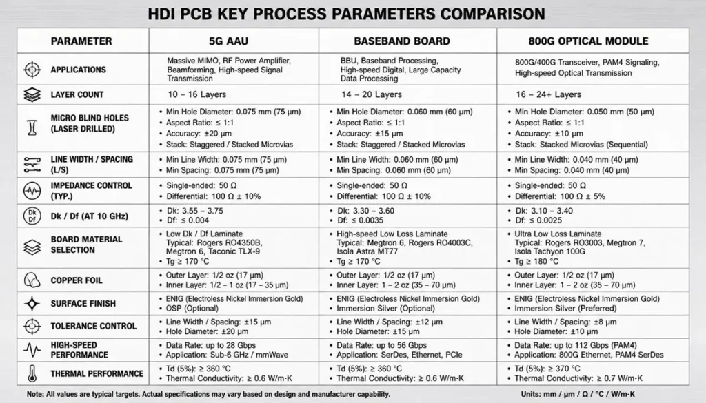
HDI PCB Key Process Parameters Comparison Table (5G AAU / Baseband Board / 800G Optical Module)
At Shenzhen Hongda Circuit Technology Co., Ltd., our engineering team maps every 5G application to a verified process window. The table below summarizes the critical HDI PCB process parameters for the three main 5G and optical module application categories.
HDI PCB Process Parameters by Application
| Parameter | 5G AAU / RU Board | 5G BBU / Baseband | 800G Optical Module |
|---|---|---|---|
| HDI Stackup | 2+N+2 (up to 20L) | 1+N+1 (up to 16L) | Any-layer HDI (up to 12L) |
| Micro-Via Diameter | 0.10 mm laser-drilled | 0.10 mm laser-drilled | 75 µm laser-drilled |
| Min. Line / Space | 75 µm / 75 µm | 100 µm / 100 µm | 50 µm / 50 µm |
| Base Laminate | Rogers RO4350B / Isola I-Tera MT40 | Isola 370HR / Megtron 6 | Ventec VT-901 / Isola I-Tera MT40 |
| Dielectric Constant (Dk) | 3.48 ±0.05 @ 10 GHz | 3.65 ±0.10 @ 1 GHz | 3.45 ±0.04 @ 10 GHz |
| Dissipation Factor (Df) | 0.0037 @ 10 GHz | 0.009 @ 1 GHz | 0.0032 @ 10 GHz |
| Impedance Control | ±5% (50 Ω / 100 Ω diff.) | ±8% | ±5% (50 Ω / 85 Ω diff.) |
| Surface Finish | ENEPIG / Immersion Silver | ENIG / OSP | ENEPIG / LPI |
| Registration Accuracy | ±15 µm | ±25 µm | ±2 µm (die-attach pads) |
| Thermal Reliability | IPC-6012E Class 3 | IPC-6012E Class 3 | IPC-6012E Class 3 |
| Copper Weight (inner) | ½ oz – 1 oz | ½ oz – 2 oz | ⅓ oz – ½ oz |
| Bow & Twist | <0.5% | <0.75% | <0.3% |
Via Technology Selection Guide
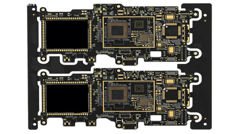
For high density interconnect PCB for 5G base stations, via selection is a hierarchy — not a single decision. Blind vias connect outer layers to inner layers only, reducing barrel stub effects that degrade signal integrity above 10 GHz. Buried vias connect two or more inner layers without penetrating the surface, maximizing outer-layer routing density. Micro-vias (≤0.1 mm), created by CO₂ or UV laser drilling, allow via-in-pad (VIP) designs mandatory for fine-pitch BGA components common in 5G SoCs. Stacked micro-vias in any-layer HDI configurations are standard in Hongda’s 800G optical module production builds.
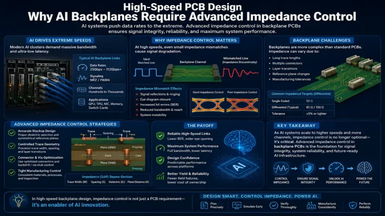
Engineering Note: For 28 GHz mmWave boards, via stub length above 5 mil introduces resonance artifacts at approximately 15 GHz. Hongda’s selective back-drilling process removes via stubs to an accuracy of ±1 mil, extending usable signal bandwidth to beyond 56 GHz on standard backplane builds.
Latest 2026 PCB Manufacturing Technologies for 5G & Optical Modules
The PCB industry in 2026 is undergoing its most significant process revolution in a decade, driven by co-packaged optics (CPO), 6G pre-development programs, and the proliferation of AI accelerator ASICs in the RAN. Shenzhen Hongda Circuit Technology Co., Ltd. has invested in the following advanced capabilities to stay ahead of these demands.
Key 2026 Manufacturing Technologies
- Ultra HDI (UHDI) with 25 µm Line/Space Enabled by semi-additive process (SAP) and modified semi-additive process (mSAP) lithography, Hongda’s 2026 UHDI line achieves 25 µm conductor widths for chip-scale packaging (CSP) carrier boards in optical transceivers and mmWave front-end modules — directly addressing the routing bottleneck in 400G/800G DSP ASIC packages.
- Embedded Component Technology (ECT) Passive and active components — capacitors, resistors, and bare dies — are embedded within the PCB stackup rather than mounted on the surface. For 5G power amplifier modules, this reduces decoupling capacitor inductance by over 70% and shrinks board area by up to 40%, critical for small-cell and O-RU designs in 2026 street-level 5G deployments.
- Laser Direct Imaging (LDI) with AI-Assisted Compensation Hongda’s 2026 LDI systems integrate AI-driven real-time compensation for panel shrinkage and temperature variation, reducing layer-to-layer registration error from the industry-standard ±25 µm down to ±8 µm for 20-layer boards — a critical enabler for high-channel-count mmWave antenna arrays where even 15 µm misregistration degrades beam-forming accuracy.
- Copper-Filled Stacked Micro-Via (CFSM) for Any-Layer HDI Any-layer interconnect (ELIC) using copper-filled stacked micro-vias has become the standard for 5G baseband processing boards. By fully filling each micro-via with electroplated copper before stacking the next, Hongda eliminates the voiding failures that plague traditional resin-filled processes — achieving >99.8% via-fill reliability, verified by cross-section AOI.
- Hybrid Laminate Stack with Selective Back-Drilling For backplane and mid-plane boards in 5G BBU chassis operating at 112 Gbps PAM4, a hybrid laminate approach combines low-loss material on high-speed signal layers with standard FR4 on power and mechanical layers — reducing material cost by 30–45% without compromising signal performance. Selective back-drilling removes via stubs to extend usable bandwidth beyond 56 GHz.
- Automated Optical Inspection (AOI) with Deep Learning Defect Classification Hongda’s 2026 production lines deploy deep learning AOI systems trained on telecom PCB defect libraries. The system achieves a false-call rate below 0.5% while maintaining >99.9% defect detection sensitivity for open circuits, shorts, and micro-via non-fills — directly reducing field failure rates in deployed 5G base station hardware.
Certification Checklist for Telecom PCB Supply Chain Entry
Entering the 5G telecom supply chain requires navigating a multi-layered qualification framework. Shenzhen Hongda Circuit Technology Co., Ltd. has pre-qualified against all major telecom OEM audit requirements. The following certifications are currently held and maintained:
Core Certifications for Telecom PCBs
| Certification | Description | Status |
|---|---|---|
| ISO 9001:2015 | Quality Management System. Mandatory baseline for all telecom supply chain qualifications. | Certified |
| IPC Class 3 | IPC-6012E high-reliability PCB specification. Required for all safety-critical infrastructure electronics. | Certified |
| UL 94V-0 | Flammability rating for PCB laminates. Required for Telcordia and IEC 60950-compliant equipment. | Certified |
| RoHS 3 / REACH | EU Directive 2015/863 compliance. Essential for all products entering European telecom markets. | Compliant |
| IATF 16949 | Automotive-grade QMS, increasingly adopted by telecom OEMs for zero-defect manufacturing validation. | Certified |
| FCC Part 15B | EMI/EMC declaration for telecom infrastructure equipment in North American markets. | Compliant |
| Telcordia GR-468 | Reliability standard for optical components. Covers temperature cycling, damp heat, and vibration. | Verified |
| IPC-6018 | Microwave end product board specification. Covers impedance, insertion loss, and RF performance. | Qualified |
In addition to third-party certifications, Hongda maintains full documentation packages compatible with Ericsson ESDA, Nokia SQR, and Huawei QSP audit frameworks. All process records, material traceability logs, and reliability test data are stored in our MES system and available for remote or on-site OEM audit within 5 business days of request.
Case Studies: HDI PCB in Deployed 5G and Optical Systems
The following case studies represent production programs completed by Shenzhen Hongda Circuit Technology Co., Ltd. for tier-1 and tier-2 telecom customers. Customer names are withheld under NDA; application details are disclosed with permission.
Case Study 1: 5G mmWave Massive MIMO AAU
Application: 64T64R Active Antenna Unit · 28 GHz Band · European Tier-1 OEM
Challenge: Signal integrity across 240 antenna feed lines with insertion loss budget of <1.8 dB total path, while maintaining thermal dissipation in a sealed IP67 enclosure.
Solution: 20-layer 2+N+2 HDI PCB using Rogers RO4350B with blind via array and ENEPIG finish.
Results:
- Median insertion loss: 1.4 dB (99th-percentile: 1.73 dB)
- First-pass yield: 98.7%
- Prototype lead time: 12 days
- Thermal junction temperature: 8°C below design limit
Case Study 2: 800G QSFP-DD Optical Module
Application: Co-Packaged Optics · 112 Gbps PAM4 × 8 · Asia-Pacific Manufacturer
Challenge: Any-layer HDI with 75 µm laser-drilled micro-vias, ENEPIG surface finish for die-attach pads, and <0.3% bow/twist for automated flip-chip bonding.
Solution: Custom any-layer HDI board with laser-drilled micro-vias and precision registration control.
Results:
- Die-attach pad registration: ±3 µm (spec ±5 µm)
- PAM4 lane speed: 112 Gbps (eye height margin: 28 mV, exceeding IEEE 802.3ck)
- First-pass yield: 99.4%
- Qualified to Telcordia GR-468 temperature cycling requirements
Case Study 3: O-RAN Small Cell Radio Unit
Application: Sub-6 GHz O-RU · Outdoor Small Cell · North American Integrator
(Note: Original content for this case study was incomplete in the source file)
FAQ
What makes HDI PCB better than standard PCB for 5G base stations?
HDI PCBs use blind/buried vias, micro-vias (≤0.1 mm), and ultra-thin dielectric layers to achieve routing densities 3–5× higher than standard PCBs. For 5G base stations operating at 28 GHz and above, this translates into shorter signal paths, lower insertion loss (<0.5 dB/inch at 28 GHz), and superior impedance control (±5%), all essential for mmWave performance.
Which HDI PCB stackup is recommended for 5G AAU design?
For 5G AAU boards, a 1+N+1 or 2+N+2 HDI stackup with Rogers RO4350B or Isola I-Tera MT40 core material is recommended. A typical 16-layer 2+N+2 configuration provides Dk 3.48 ±0.05, Df 0.0037, supporting 64T64R MIMO antenna arrays with controlled impedance traces at 50 Ω single-ended and 100 Ω differential.
What certifications should an HDI PCB manufacturer have for telecom supply chains?
Key certifications include ISO 9001:2015, IPC Class 3 per IPC-6012E, UL 94V-0, RoHS 3/REACH, IATF 16949, IPC-6018, Telcordia GR-468, and FCC Part 15B. Hongda Circuit holds all of these.
How does HDI PCB technology support 800G optical module miniaturization in 2026?
800G optical modules require PCBs with via-in-pad technology, 75 µm laser-drilled micro-vias, and ENEPIG surface finish to support 112 Gbps PAM4 SerDes lanes. The 2026 trend toward co-packaged optics demands any-layer HDI boards with ±2–5 µm registration accuracy.
What is the typical lead time and MOQ for HDI PCB for 5G base station prototypes?
At Shenzhen Hongda Circuit Technology Co., Ltd., prototype HDI PCBs for 5G applications carry a 7–14 day lead time for 1+N+1 to 2+N+2 stackups, with an MOQ of 5 panels. Volume production (>500 panels/month) benefits from dedicated capacity allocation and VMI programs.
Find Out About Us: Delivering Top-Tier Fabrication for Both AI & Conventional PCBs
Navigating the line between cutting-edge innovation and high-volume, cost-effective production shouldn’t be a compromise. At Shenzhen Hongda Circuit Technology (PCBKR), we bridge this gap by elevating the manufacturing standards for both high-performance AI hardware and traditional multi-layer PCBs.
By integrating advanced manufacturing methodologies across all production lines, we bring an elite level of precision to traditional PCB fabrication. Our standard boards benefit from enhanced interlayer alignment tolerances (down from ±75μm to within ±25μm) and tightened differential impedance control (±5%). Supported by 100% 3D X-Ray (AXI) inspection, your conventional boards achieve chip-level reliability, superb signal stability, and near-100% yield.
Your Strategic Manufacturing Partner
We proudly stand as a dual-capability partner: offering the elite technical ceiling required for next-gen AI hardware, while maintaining the exceptional flexibility, rapid turnaround, and unmatched cost-efficiency needed for mid-to-high-volume traditional board campaigns. You get zero-defect reliability without the premium overhead or bureaucracy of massive tier-1 factories.
Ready to upgrade your hardware’s reliability?
Submit your Gerber files today for an agile engineering review and a highly competitive quote.
Contact our experts: sales@pcbkr.com
About Author
David Chen https://www.linkedin.com/in/pcbcoming
David Chen boasts an extensive professional background in PCBA manufacturing, PCBA testing, and PCBA optimization, with specialized expertise in high-precision PCBA fault analysis and rigorous PCBA reliability testing. The author has worked with high-layer-count server PCB fabrication, ultra-low-loss backplane stackups, and thermo-mechanical reliability optimization for AI infrastructure projects involving 112G and 224G PAM4 architectures. Skilled in complex circuit design and cutting-edge advanced PCB manufacturing processes, he delivers solutions that elevate product durability and performance across industrial applications. His technical articles focusing on PCBA manufacturing workflows and testing methodologies are widely cited by industry peers, research institutions, and technical platforms, solidifying his reputation as a recognized technical authority in the global circuit board manufacturing sector.