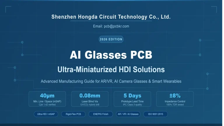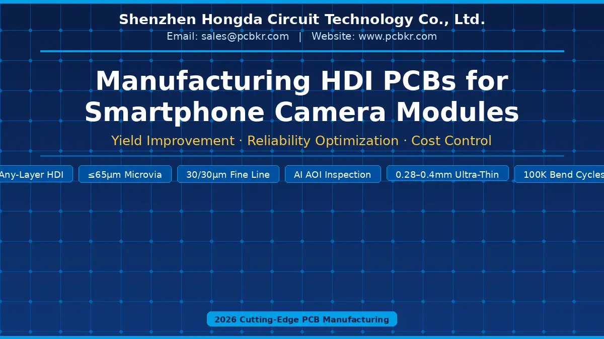
Manufacturing HDI PCBs for Smartphone Camera Modules: Yield Improvement, Reliability Optimization & Cost Control
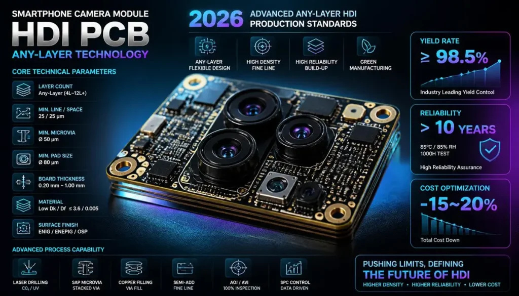
2026 Any-Layer HDI PCB Technical Specs for Smartphone Camera Modules
Why Any-Layer HDI Is Indispensable for Modern Smartphone Camera Systems
Driven by multi-camera arrays, OIS anti-shake, ToF depth sensing, foldable flagship phones and 5G/6G high-frequency communication, smartphone PCBs have evolved toward ultra-thin, ultra-dense, multi-functional integration by 2026. Traditional stepwise blind-buried HDI can no longer meet the wiring demands of 4–6 camera modules with high-speed MIPI CSI signals, making Any-Layer HDI the core substrate for flagship imaging hardware.
Classic HDI only realizes interlayer connection through sequential blind holes with limited routing flexibility, while Any-Layer HDI enables laser microvia interconnection between every layer via stacked and staggered vias. For 2026 new smartphone products, multi-lens camera modules require 10–16 layer ultra-fine line HDI substrates under 0.4mm thickness, coupled with foldable bending resistance and strict high-frequency impedance control. As a professional HDI PCB manufacturer, Shenzhen Hongda Circuit Technology Co., Ltd. deploys 2026 cutting-edge PCB manufacturing processes to resolve core pain points of OEMs, camera module designers and procurement teams.
Core Pain Points Faced by Smartphone Camera Module Buyers & Hardware Engineers
We summarize the universal bottlenecks encountered during NPI and mass production of camera HDI PCBs, and match our 2026 advanced technologies to deliver targeted solutions:
- Ultra-high integration of multi-camera hardware: Multi-lens + OIS + ToF generate dense MIPI high-speed signal crosstalk, conventional PCB layouts cause EMI interference and image distortion.
- Ultra-thin substrate limitation: Camera core PCB thickness ≤0.4mm brings copper cracking, layer delamination and low production yield risks.
- Foldable device bending reliability: Flexible hinge zones suffer repeated bending fatigue, prone to microvia fracture and open circuits after thousands of folds.
- 5G/6G RF high-frequency performance demands: Poor impedance control and high signal loss degrade millimeter-wave antenna and wireless module performance.
- Short NPI cycle & fast RFQ pressure: Brands launch new camera iterations annually, requiring 24–72h fast quotation, rapid prototyping and synchronous DFM feedback.
2026 Cutting-Edge Any-Layer HDI Manufacturing Technologies Deployed by Hongda Circuit
To tackle the above challenges, our factory fully upgraded production lines with 2026 industry-leading processes exclusive for smartphone camera HDI:
1.Ultra-precision Composite Laser Drilling Tech
Adopt UV+CO₂ dual-beam composite laser equipment, positioning accuracy controlled within 8μm (beyond the traditional 10μm threshold). Realize microvias ≤65μm (down from 75μm standard), supporting stacked staggered via structures for 12–16 layer camera mainboards. Laser drilling void rate reduced by 40% to eliminate microvia failure in tiny camera substrates.
2.Ultra-fine Line LDI Direct Imaging Process 2026
New-generation high-resolution LDI machines achieve line width/space 30/30μm (surpassing 40/40μm mainstream capacity). Optimize MIPI CSI high-speed signal routing density for triple/quad camera modules, reserve complete EMI shielding ground layers to suppress imaging noise.
3.Ultra-thin Low Dk/Df High-Frequency Material Lamination
2026 new low-loss MPI/LCP hybrid thin copper foil (3μm ultra-thin low-roughness copper) matched with halogen-free ultra-thin core substrates. Complete rigid ultra-thin HDI (0.28–0.4mm) and rigid-flex PCB production lines, effectively solve CAF migration and layer separation risks under thin thickness.
4.AI Full-Process Inspection System
Upgrade 2026 intelligent AOI + 3D X-Ray automatic detection platform. AI algorithm automatically identifies hidden hole voids, copper cracks and micro-shorts in camera PCBs; real-time data feedback adjusts laser and electroplating parameters to stabilize mass production yield above 96%.
5.Low-cost DFM Intelligent Simulation Platform
Self-developed SI/PI/mechanical bending simulation software launched in 2026. Conduct pre-production simulation for impedance, signal integrity and bending fatigue of camera modules, simplify redundant stacked via structures without sacrificing performance to cut raw material and laser processing costs.
Targeted Solutions for Smartphone Camera Module HDI PCB Design
Combined with 2026 process upgrades, we provide full-lifecycle design optimization for camera imaging substrates:
- High-speed MIPI Signal Layout Optimization: Partition independent signal layers for ISP image processing chips, add complete reference ground layers to isolate EMI; use low-roughness copper foil to reduce high-speed signal attenuation and avoid picture flickering.
- Ultra-thin & Foldable Reliability Design: For foldable camera modules, adopt segmented rigid-flex transition zones, set stress relief grooves in bending areas; our 2026 lamination process improves bending cycle life to over 100,000 times without copper fracture.
- Thermal & Microvia Failure Prevention: Add embedded thermal copper pads under ISP chips for heat dissipation; adopt pulse electroplating to eliminate hole wall voids, solving thermal expansion induced microvia cracking in compact camera modules.
- Mass Production DFM Support: Our engineering team delivers free DFM reports within 12 hours after receiving Gerber files, optimize layer stacking, via layout and line width to balance yield and manufacturing cost for prototype and mass production phases.
Manufacturing Yield Improvement & Reliability Control System (2026 Standard)
Yield loss and reliability failure are the top two cost killers for camera HDI. Hongda Circuit builds a closed-loop quality control system with 2026 new technologies:
- Laser process yield lifting: Composite laser positioning correction reduces misalignment scrap; real-time monitoring of laser ablation depth cuts microvia reject rate by 35%.
- Electroplating reliability upgrade: Add vertical pulse electroplating lines for microvias, hole wall copper thickness uniformity ±2μm, avoid void lamination and thermal cycling failure.
- Multi-dimensional reliability testing: Standard environmental tests including thermal shock (-40℃~125℃), humidity aging, bending fatigue, CAF resistance; all camera HDI samples pass full certification before mass shipment.
- AI quality traceability: Each PCB batch binds laser drilling, imaging, AOI and X-Ray data, fast locate defective root causes to continuously boost mass production yield.
Cost Control Strategies for Any-Layer HDI Camera PCBs
Based on 2026 process iteration experience, we help customers cut comprehensive PCB costs without sacrificing camera module performance:
- Simplify stacking via DFM simulation: Reduce unnecessary stacked vias and extra layers where signal performance allows, lower laser processing frequency (the primary cost driver of Any-Layer HDI).
- Material tiered matching: Recommend cost-effective standard low-Dk materials for mid-range camera modules; allocate high-end LCP/MPI only for flagship 6G millimeter-wave models to avoid over-spec raw material expenditure.
- Yield-driven cost reduction: AI inspection reduces post-production rework scrap; stable high yield directly lowers unit amortized cost for mass orders above 100k pcs.
- Separate prototype & mass production lines: Independent fast NPI prototyping lines avoid occupying mass production capacity, shorten lead time without premium surcharges for small-batch pre-production.
Fast RFQ & NPI Service Flow for Smartphone OEM Purchasers
To resolve customers’ short-cycle rapid quotation demands, Hongda Circuit launches standardized fast service process tailored for camera module projects:
Customers only need to submit the following documents to obtain a formal quotation within 24–72 hours:
- Complete Gerber files + layer stack-up drawing
- Strict impedance tolerance requirements (±3%~±5%)
- Camera module interface dimension & pin definition
- Constraints of board thickness, overall size and foldable bending range
- Production volume forecast (NPI prototype / mass production MP)
Value-added free services included: confidential NDA signing, full DFM risk assessment, SI high-speed signal simulation, and one-to-one dedicated technical engineer follow-up throughout NPI to mass production.
Why Choose Shenzhen Hongda Circuit Technology Co., Ltd. for Camera HDI PCBs
- Mature mass production experience on 10–16 layer Any-Layer HDI for 2026 flagship multi-camera, OIS and foldable smartphone projects.
- Full 2026 upgraded production equipment: dual-beam composite laser drills, high-precision LDI, 3D AI X-Ray inspection equipment.
- Specialized R&D team for imaging module HDI, proficient in MIPI high-speed signal, EMI control and foldable rigid-flex reliability design.
- Balanced capability for small-batch NPI prototyping and large-volume mass manufacturing, flexible to match smartphone brand iterative launch cycles.
- Closed-loop yield & cost management system, transparent cost breakdown and stable delivery timeline for global electronic procurement teams.
As smartphone camera hardware evolves toward multi-lens ultra-thin foldable designs and 6G high-frequency communication, Any-Layer HDI PCB becomes the foundational carrier determining imaging quality, equipment reliability and overall BOM cost. Leveraging 2026 cutting-edge composite laser drilling, ultra-fine line LDI and AI intelligent inspection technologies, Shenzhen Hongda Circuit Technology Co., Ltd. comprehensively addresses pain points of low yield, poor bending reliability, high signal loss and uncontrollable manufacturing costs for camera module clients.
If you are developing new smartphone camera modules, submit your Gerber files and technical specifications now to receive free DFM optimization suggestions and competitive fast quotation from our professional engineering team.
HDI PCBs for Smartphones FAQ
What key technical capability indicators should I verify from HDI PCB manufacturers for smartphone multi-camera modules?
What key technical capability indicators should I verify from HDI PCB manufacturers for smartphone multi-camera modules? A: Focus on four core indicators: 1) Minimum microvia size and laser positioning accuracy (2026 mainstream standard ≤65μm via, positioning tolerance <8μm); 2) Finest achievable line width/space (flagship camera modules require at least 30/30μm); 3) Mass production yield of 0.4mm ultra-thin Any-Layer HDI (stable yield ≥95% for qualified suppliers); 4) Rigid-flex bending cycle life for foldable camera parts (over 100,000 times without open circuit). We provide official test reports and batch yield data for customer audit.
Our quad camera HDI has severe MIPI signal crosstalk and image noise, what design and manufacturing solutions can suppliers provide in 2026?
Two optimized technical paths: 1) Design side: Our engineers conduct free SI simulation to partition independent high-speed signal layers and add continuous complete ground shielding layers; 2) Manufacturing side: Adopt 2026 low-roughness 3μm ultra-thin copper foil composite laser process, reduce high-frequency signal attenuation and EMI interference, effectively eliminate camera screen flickering and color distortion caused by crosstalk.
How can suppliers help us cut HDI PCB costs without downgrading camera module performance in mass production?
We adopt 2026 DFM intelligent simulation for cost optimization: simplify redundant stacked via structures, match graded high-frequency materials according to product positioning, improve mass production yield via AI full-process inspection to reduce scrap loss. Meanwhile, we separate prototype and mass production lines to avoid capacity premium, and offer volume tiered pricing for orders above 50,000 pieces.
Our foldable front camera PCB is prone to copper cracking and microvia fracture after repeated bending, what 2026 new manufacturing processes solve this reliability risk?
Our 2026 upgraded rigid-flex lamination process uses ultra-low-modulus prepreg and stress relief groove design for bending zones; pulse electroplating ensures uniform copper thickness on microvia walls to avoid thermal-mechanical fatigue cracks. All samples complete 100,000-time bending fatigue testing before mass production, with full reliability test reports provided.
What documents do we need to prepare for fast RFQ and NPI DFM feedback, and how long is the quotation lead time of your factory?
Required documents: Gerber files, layer stack-up drawing, impedance specs, camera module size/thickness limits, annual production forecast. Our standard service delivers formal quotation within 24–72 hours and free DFM risk report within 12 hours. We support confidential NDA signing and assign dedicated technical engineers to track the whole NPI iteration cycle for new smartphone camera projects.
Find Out About Us: Delivering Top-Tier Fabrication for Both AI & Conventional PCBs
Navigating the line between cutting-edge innovation and high-volume, cost-effective production shouldn’t be a compromise. At Shenzhen Hongda Circuit Technology (PCBKR), we bridge this gap by elevating the manufacturing standards for both high-performance AI hardware and traditional multi-layer PCBs.
By integrating advanced manufacturing methodologies across all production lines, we bring an elite level of precision to traditional PCB fabrication. Our standard boards benefit from enhanced interlayer alignment tolerances (down from ±75μm to within ±25μm) and tightened differential impedance control (±5%). Supported by 100% 3D X-Ray (AXI) inspection, your conventional boards achieve chip-level reliability, superb signal stability, and near-100% yield.
Your Strategic Manufacturing Partner
We proudly stand as a dual-capability partner: offering the elite technical ceiling required for next-gen AI hardware, while maintaining the exceptional flexibility, rapid turnaround, and unmatched cost-efficiency needed for mid-to-high-volume traditional board campaigns. You get zero-defect reliability without the premium overhead or bureaucracy of massive tier-1 factories.
Ready to upgrade your hardware’s reliability?
Submit your Gerber files today for an agile engineering review and a highly competitive quote.
Contact our experts: sales@pcbkr.com
About Author
David Chen https://www.linkedin.com/in/pcbcoming
David Chen boasts an extensive professional background in PCBA manufacturing, PCBA testing, and PCBA optimization, with specialized expertise in high-precision PCBA fault analysis and rigorous PCBA reliability testing. The author has worked with high-layer-count server PCB fabrication, ultra-low-loss backplane stackups, and thermo-mechanical reliability optimization for AI infrastructure projects involving 112G and 224G PAM4 architectures. Skilled in complex circuit design and cutting-edge advanced PCB manufacturing processes, he delivers solutions that elevate product durability and performance across industrial applications. His technical articles focusing on PCBA manufacturing workflows and testing methodologies are widely cited by industry peers, research institutions, and technical platforms, solidifying his reputation as a recognized technical authority in the global circuit board manufacturing sector.