Aluminum PCB in 2026: What’s Changed in Manufacturing,Design, and Enclosure Integration
Aluminum box PCB: Buyers researching an aluminum PCB manufacturer in 2026 are no longer comparing bare boards side by side. Thermal performance, enclosure integration, and turnkey assembly capability have become the real differentiators, and the manufacturing floor behind an aluminum circuit board has changed more in the last two years than in the previous decade. This article walks through what’s driving that shift, how a modern aluminum PCB board is actually built today, and where an integrated aluminum box PCB solution fits into a sourcing strategy.
Shenzhen Hongda Circuit Technology Co., Ltd. produces aluminum PCBs, metal core PCBs
(MCPCB), and fully assembled aluminum box PCB modules for LED lighting, power
electronics, and industrial control applications. The observations below come from what
we’re seeing on our own lines and hearing from engineering teams placing orders.
What Is an Aluminum PCB, and Why Does the Definition Keep Expanding
An aluminum PCB — sometimes shortened to alu pcb, and written as aluminium pcb in UK
English sourcing documents — is a circuit board built on a metal-clad laminate rather than
standard FR-4. A thin dielectric layer sits between the copper circuit and the aluminum
base, conducting heat away from components while the aluminum substrate acts as both
structural support and heat spreader.
That definition used to be enough. It isn’t anymore. Buyers today are asking a broader
question: what is aluminum pcb capable of when it’s designed alongside the enclosure it
sits inside, not just as an isolated component. That’s the gap between a traditional
aluminum pcb board supplier and what’s now being called an aluminum box PCB program
— where the metal core board and the aluminum enclosure are engineered together as one
thermal and mechanical system.
Aluminum PCB Manufacturing Technology in 2026: Four Shifts Worth Knowing
Higher Thermal Conductivity Dielectric Materials
Standard aluminum PCB dielectric layers have historically topped out around 1.0–2.0W/mK. Material suppliers have pushed that ceiling higher through ceramic-filled and ceramic-ester dielectrics, with production-grade options now reaching 3.0–5.0+ W/mK without sacrificing dielectric breakdown strength. For high-power LED and power-module designs, that difference changes what copper thickness and board size are needed to hit a target junction temperature — often allowing a smaller aluminum pcb boards footprint for the same thermal budget.
Laser Drilling and mSAP for Finer Circuitry on Metal Core Boards
Mechanical drilling and standard subtractive etching limit how fine a trace and via structure can go on a metal-backed laminate. Laser micro-via drilling combined with modified semi-additive processing (mSAP) is now reaching aluminum and metal core pcb / pcb constructions that were previously reserved for rigid FR-4 HDI boards. This matters for AI hardware modules and compact power supplies where component density has increased faster than board real estate.
Simulation-Led Thermal Design Before the First Sample
Rather than building a prototype and measuring thermal performance after the fact, thermal simulation is now run at the layout stage — modeling the full path from junction to ambient air, including the dielectric layer, base metal, and (where applicable) the enclosure itself. This shortens the design-to-first-sample cycle and reduces the number of respin iterations a buyer has to pay for.
Halogen-Free and Higher-Reliability Base Materials
Environmental compliance requirements (RoHS, REACH, and increasingly customer specific halogen-free mandates) have pushed dielectric and solder mask chemistry toward halogen-free formulations that also happen to offer better long-term thermal cycling performance — a case where regulatory pressure and engineering performance have moved in the same direction.
Aluminum Box PCB: Where Circuit Board and Enclosure Design Converge
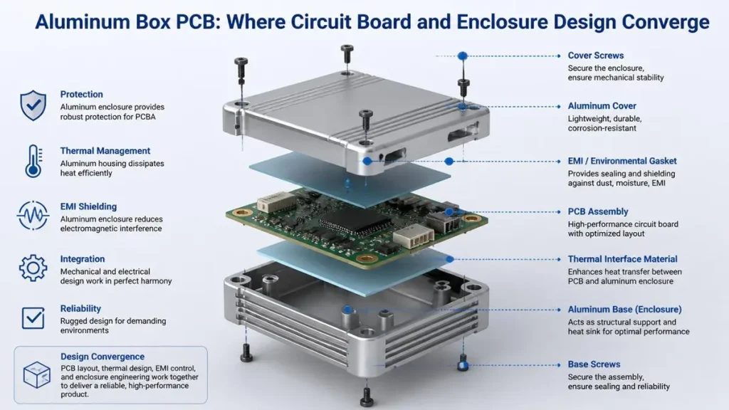
Exploded view of the aluminum box pcb system demonstrating design convergence.
This 3D diagram details how the PCB layout, thermal interface material (TIM), and aluminum housing are integrated together for optimal EMI shielding, mechanical stability, and environmental protection.
An aluminum box pcb solution combines three elements that are traditionally sourced and
engineered separately: the aluminum-clad circuit board, the aluminum enclosure, and the
thermal interface material (TIM) that connects them. Sourcing all three from one supplier collapses a fragmented supply chain into a single point of accountability, which is increasingly the reason procurement teams request it.
The Thermal Path, End to End
The End-to-End Heat Dissipation Process of an Aluminum Box PCB System
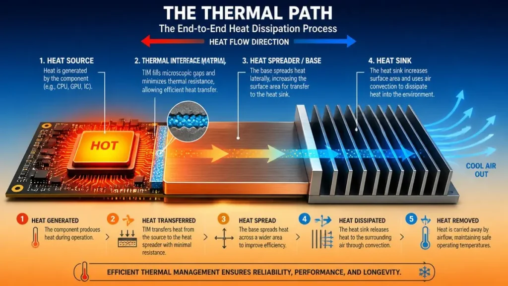
This diagram illustrates the complete thermal path—modeling how heat flows efficiently from the high-power component through the TIM, across the aluminum substrate, and out through the integrated enclosure’s cooling fins.
Heat generated at the component doesn’t stop at the edge of the circuit board. The full path
runs from the heat source, through the aluminum substrate, across the interface material,
into the enclosure wall, and finally out to ambient air. Designing the aluminum pcb and the
aluminum box together means each stage of that path — dielectric conductivity, base metal
thickness, TIM selection, and enclosure fin geometry — is optimized as one system instead
of four separately-sourced guesses.
Mechanical and DFM Coordination
Dimensional tolerance between the board and enclosure, mounting method (screw-down,
snap-fit, or adhesive), and ingress protection (IP-rated sealing against dust and moisture)
all have to be resolved before tooling is cut. Handling this at the design-for-manufacturing
stage — rather than after the enclosure is already tooled — avoids the rework that happens
when a board supplier and an enclosure vendor never actually talked to each other.
Turnkey Assembly: From Bare Board to Finished Module
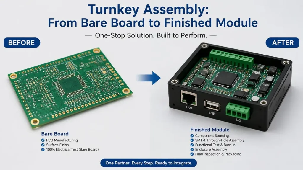
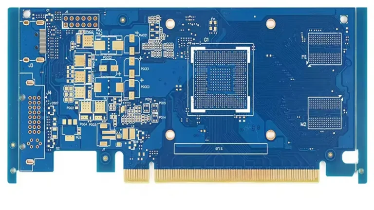
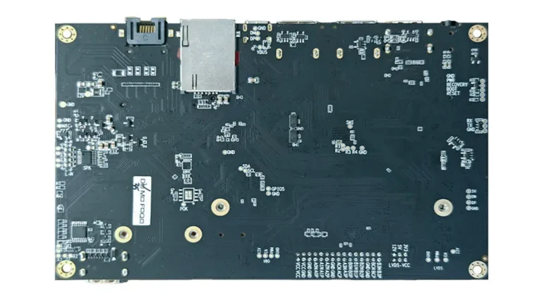
Turnkey aluminum box pcb manufacturing workflow. A direct comparison showing the transition from a fabricated bare aluminum board to a fully populated, tested, and enclosed electronic module under a single point of accountability.
A turnkey aluminum box pcb program typically covers aluminum-based PCB fabrication,
BOM sourcing, SMT/DIP assembly, aluminum enclosure processing (CNC machining,
extrusion, or die-casting), and final module assembly and test. The practical benefit for a
buyer is fewer vendors, fewer shipping legs between sub-suppliers, and one quality record
instead of three
Choosing Materials: What Actually Affects Aluminum PCB Board Performance
Not every “aluminum pcb manufacturer” quote is comparing the same thing. Three
variables account for most of the price and performance spread between suppliers:
1. Dielectric layer thickness and conductivity — thinner isn’t automatically better; it’s
a trade-off against dielectric breakdown voltage.
2. Copper weight — heavier copper improves current-carrying capacity and heat
spreading across the board plane, at a material cost premium.
3.Base aluminum alloy and enclosure surface treatment — anodizing, powder
coating, and conductive oxidation each change thermal emissivity and corrosion
resistance differently, which matters for outdoor LED and industrial enclosures.
Where Aluminum PCB and Aluminum Box PCB Are Being Used in 2026
High-power LED lighting modules remain the largest application for metal core pcb technology, but the fastest-growing demand is coming from AI hardware power modules, EV charging electronics, and industrial control units — all applications where component density and heat density are rising together. In each case, the question buyers are asking has shifted from “can you make an aluminum pcb board” to “can you make one that survives inside a sealed, finned enclosure at full load for ten years.”
Why Buyers Are Vetting Aluminum PCB Manufacturers Differently
A supplier that only fabricates bare aluminum circuit boards can still be the right choice for
a buyer who already owns enclosure design and assembly in-house. But for teams trying to
reduce supplier count and shorten lead time, the aluminum box pcb / turnkey model is
becoming the default request in RFQs. Shenzhen Hongda Circuit Technology Co., Ltd. supports both models — standalone aluminum PCB board fabrication, and fully integrated aluminum box PCB design, thermal simulation, and assembly — so the scope can match how a buyer’s team is actually structured.
Frequently Asked Questions from Procurement Teams Researching Aluminum PCB Suppliers
What’s the difference between an aluminum PCB and a standard FR-4 PCB?
An aluminum PCB replaces the FR-4 core with a thermally conductive dielectric layer bonded to an aluminum base. It’s chosen when a design needs to move heat away from components efficiently — FR-4 alone can’t do that. Standard FR-4 remains the better (and cheaper) choice for low-power, low-heat circuits.
How do I know what thermal conductivity dielectric I actually need?
It depends on power density and target junction temperature, not on picking the highest number available. A reliable manufacturer will ask for your power dissipation figures and run a thermal calculation before recommending a dielectric spec, rather than defaulting to the most expensive option.
Can one supplier really handle both the aluminum PCB and the enclosure?
Yes, where the supplier has in-house or tightly integrated CNC, extrusion, or die-casting capability alongside PCB fabrication and SMT assembly. Ask to see examples of completed aluminum box PCB modules, not just bare boards, before assuming a supplier can manage both.
What lead time should I expect for a custom aluminum box PCB program versus a standard aluminum PCB order?
A standalone aluminum PCB order is generally faster since it skips enclosure tooling and joint mechanical design. A full aluminum box PCB
program adds time for DFM review between board and enclosure, but usually saves total project time compared to coordinating a PCB vendor and an enclosure vendor separately.
What should I send a supplier to get an accurate aluminum PCB quote?
At minimum: Gerber files (or PCB design files), a bill of materials, target copper weight and dielectric conductivity if known, and — for aluminum box PCB requests — the mechanical enclosure files (STEP format) or a description of the intended enclosure so thermal and mechanical design can be reviewed together rather than quoted blind.
About Author
David Chen https://www.linkedin.com/in/pcbcoming
David Chen boasts an extensive professional background in PCBA manufacturing, PCBA testing, and PCBA optimization, with specialized expertise in high-precision PCBA fault analysis and rigorous PCBA reliability testing. The author has worked with high-layer-count server PCB fabrication, ultra-low-loss backplane stackups, and thermo-mechanical reliability optimization for AI infrastructure projects involving 112G and 224G PAM4 architectures. Skilled in complex circuit design and cutting-edge advanced PCB manufacturing processes, he delivers solutions that elevate product durability and performance across industrial applications. His technical articles focusing on PCBA manufacturing workflows and testing methodologies are widely cited by industry peers, research institutions, and technical platforms, solidifying his reputation as a recognized technical authority in the global circuit board manufacturing sector.