How Is an Aluminum PCB Made? A 2026 Step-by-Step FactoryGuide to Modern Metal Core PCB Manufacturing
How is an aluminum PCB made? Engineers rarely ask this question out of idle curiosity. Most of the time they are staring at a thermal simulation that refuses to cooperate, or a return list full of LED drivers that failed early in the field. Understanding the manufacturing process of aluminum PCBs — not just what an aluminum PCB is — is what lets a design team catch problems before the first prototype run, rather than after.
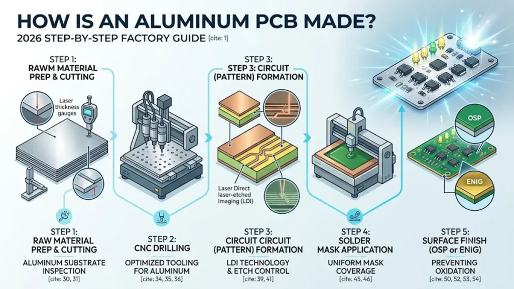
How Is an Aluminum PCB Made – Full Aluminum Substrate Fabrication Process Infographic
This guide walks through the factory floor at Shenzhen Hongda Circuit Technology Co., Ltd., station by station, from raw sheet metal to a finished aluminum PCB board ready for surface-mount assembly. Along the way, we point out where 2026’s process upgrades — laser imaging, AI-assisted optical inspection, and tighter dielectric control — have changed what a “standard” metal core PCB can do, and where a few minutes of design-for manufacturing (DFM) review can save weeks of rework later.
What Is an Aluminum PCB? The Basics Behind Metal Core PCB Construction
An aluminum PCB (also called an aluminum circuit board, alu PCB, or — using its formal industry name — a metal core PCB, MCPCB) replaces the fiberglass core of a standard FR4 board with a solid aluminum substrate. The stack-up is simple in concept: a copper circuit layer on top, a thermally conductive dielectric layer in the middle, and an aluminum (or occasionally copper) base underneath.
That aluminum base isn’t decorative. It exists to pull heat away from LEDs, MOSFETs, and power ICs far faster than epoxy-glass ever could, which is why aluminum PCBs dominate LED lighting fixtures, motor drivers, power supplies, and increasingly, automotive and EV power modules where component density keeps climbing every year.
Because the construction is different from FR4, the manufacturing rules are different too — and that’s the part most buyers never see until something goes wrong.
Aluminum PCB vs. FR4: Why the Metal Base Changes Everything
A conventional FR4 board and an aluminum PCB board look similar on a spec sheet until you get to thermal resistance. The dielectric layer on a metal core board is engineered specifically to conduct heat vertically into the aluminum base, while still providing electrical isolation between the copper trace and the metal core.
That single design requirement cascades into everything downstream: Drilling has to account for a harder, more thermally conductive base material that wears tooling differently than woven glass fiber. Etching has to protect fine copper geometry without undercutting traces bonded to a
dielectric that behaves differently under heat and chemistry than standard prepreg. Surface finish selection changes depending on whether the board will see repeated reflow cycles or a single assembly pass.
None of this is exotic, but it does mean an aluminum PCB manufacturer needs process
controls tuned specifically for metal-backed substrates — not just an FR4 line running
aluminum panels through it.
Inside the Factory: The Aluminum PCB Board Manufacturing Process, Step by Step
At a high level, an aluminum circuit board moves through five core stages before it reaches
final inspection:
- Material preparation and cutting
- Drilling
- Circuit (pattern) formation
- Solder mask application
- Surface finish
Below is what actually happens at each station, along with the DFM notes our engineering
team flags most often when reviewing customer Gerber files.
Step 1 — Cutting and Material Preparation
Every aluminum PCB board starts as a raw panel selected to match the board outline in the
customer’s Gerber data. Panels are inspected on arrival for thickness consistency and
surface condition before CNC cutting or panel shearing brings them down to working size.
DFM tip: Leave adequate panel margin and spacing between boards during
array/panelization. Aluminum substrates are less forgiving of tight edge clearances than
FR4 — cutting too close to the copper can invite shorts or edge burrs that show up later in
testing.
Step 2 — Drilling the Aluminum Circuit Board
CNC drilling machines cut mounting holes, plated through-holes, and signal vias into the
panel. Aluminum’s hardness and thermal conductivity wear drill bits faster than fiberglass,
so hole-wall quality and bit life are watched closely at this stage, with tooling swapped on a
tighter schedule than a standard FR4 line would require.
DFM tip: Standardizing hole diameters wherever the schematic allows reduces tool
changes and keeps hole-position accuracy tight across the panel. Designers should also
double-check pad-to-via clearance so solder paste can’t wick into an open via during reflow.
Step 3 — Circuit Layer Formation: How an Aluminum PCB Gets Its Traces
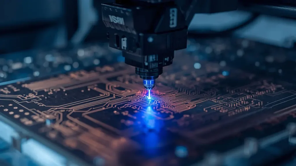
Laser Direct Imaging (LDI) in Action. Modern 2026 metal core PCB lines utilize high-precision LDI systems to trace fine circuit geometries directly onto the copper layer, bypassing older film phototools to eliminate registration errors and thermal hot spots
This is the step most people picture when they ask “how is an aluminum PCB made.”
Copper foil is laminated to the dielectric, cleaned, and imaged — increasingly by laser
direct imaging (LDI) rather than older photo-tool exposure — before the panel goes
through developing and etching to leave only the copper pattern from the customer’s
design.
DFM tip: Trace width and spacing have to match what the etch line can reliably hold on a
metal-backed panel. Sharp interior corners are worth avoiding altogether; they concentrate
etchant and accelerate localized copper attack, which is a common root cause of
intermittent trace failures on aluminum boards specifically.
Step 4 — Solder Mask Application on the Aluminum PCB Board
Once the circuit layer is verified, solder mask ink is applied and cured, then selectively
exposed and developed to open pad areas while protecting the rest of the copper. Mask
thickness and edge coverage are checked before the panel moves on.
DFM tip: Solder mask dams between closely spaced pads need enough width to actually
survive the exposure and development process — too narrow, and adjacent pads can bridge
during assembly. Mask should never encroach onto the pad itself, or soldering quality
suffers.
Step 5 — Surface Finish: OSP or ENIG for Aluminum PCBs
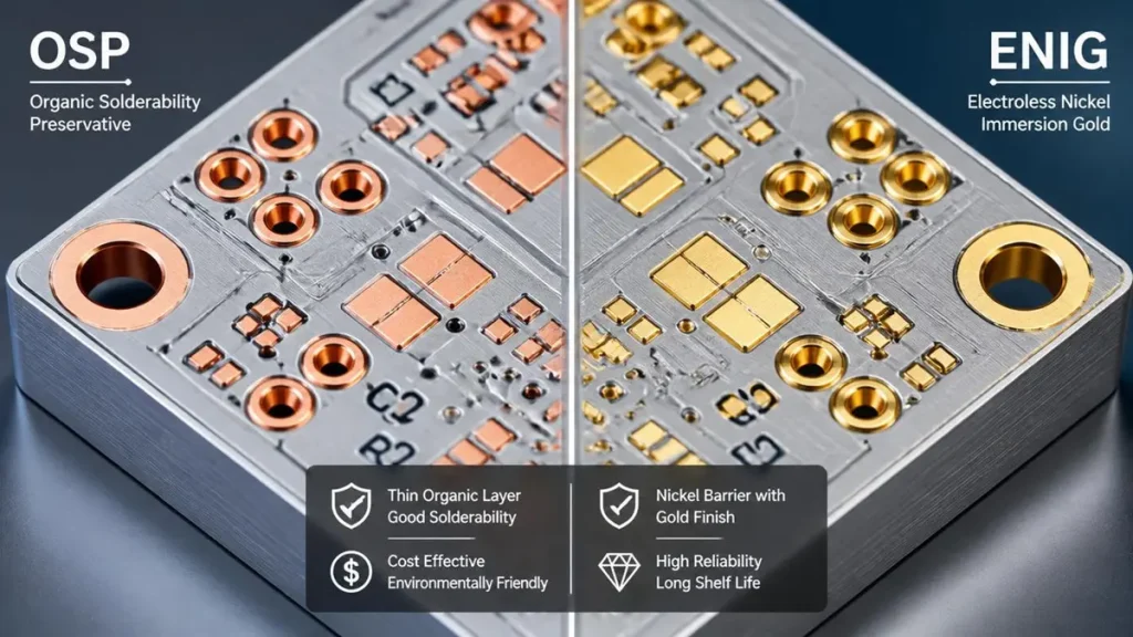
Aluminum PCB Surface Finish Options: OSP vs. ENIG
The final protective layer goes onto the exposed copper pads to prevent oxidation and keep
them solderable. Two finishes cover the overwhelming majority of aluminum PCB orders:
1. OSP (Organic Solderability Preservative) — a thin organic coating suited to single
pass reflow assembly and cost-sensitive volume production.
2. ENIG (Electroless Nickel Immersion Gold) — a nickel-gold finish that holds up
through multiple reflow cycles and offers a flatter, more durable pad surface for fine
pitch or high-reliability components.
DFM tip: Specify the surface finish explicitly in the BOM, not just in the Gerber notes.
Mismatches between what was quoted for prototyping and what’s assumed for mass
production are a surprisingly common source of last-minute schedule slips.
What’s New in 2026: Aluminum PCB and Metal Core PCB Manufacturing Technology
A few shifts have moved from “advanced option” to “standard expectation” on modern
aluminum PCB lines:
Laser Direct Imaging and AI-Assisted Optical Inspection
LDI has largely replaced film phototools for circuit patterning, tightening line-width and
registration tolerances on aluminum circuit boards without adding cost at typical order
volumes. On the inspection side, AI-driven AOI systems now flag copper-edge irregularities
and etch anomalies earlier and more consistently than manual visual checks — which
matters more on metal core boards, where a marginal etch defect can turn into a thermal
hot spot rather than just a cosmetic flaw.
Higher-Performance Dielectric and Alloy Options
Dielectric materials with improved thermal conductivity ratings are now common even on
mid-volume orders, letting designers push higher current density onto a given board area
without redesigning the whole thermal path. On the metal side, alloy selection has become
more deliberate: general-purpose 1100/3003 aluminum still covers most LED and
commodity applications, while higher-strength alloys are increasingly specified for boards
that double as a structural chassis or enclosure — an aluminum box PCB, in industry
shorthand — rather than a flat board mounted inside a separate housing.
Tighter DFM Feedback Loops
The biggest practical change for buyers isn’t a single machine — it’s how early DFM
feedback happens. Automated Gerber checks now catch aluminum-specific issues (edge
clearance, via-in-pad conflicts, mask dam width) before a panel is ever cut, instead of after a
failed first article. For procurement teams, that means fewer surprise re-spins between
prototype and production.
How to Solder Aluminum PCB Boards Without Damaging the Substrate
Because the aluminum base draws heat away from the joint so efficiently, soldering an
aluminum PCB by hand typically needs a higher iron temperature and a longer, steadier
dwell time than an FR4 board of similar pad size — the heat sink effect of the metal core
pulls thermal energy away from the joint faster than it would on fiberglass. For reflow
assembly, profile settings should be validated against the specific dielectric and copper
weight in use rather than reused from an FR4 profile, since ramp and soak times that work
fine on glass-epoxy can under- or overheat a metal-backed board. Getting this wrong
doesn’t usually show up as a visible defect immediately — it shows up as an intermittent
joint months later.
Choosing a Reliable Aluminum PCB Manufacturer: What to Verify Before You Order
When evaluating an aluminum PCB manufacturer, a few questions separate a transparent,
process-controlled supplier from one that’s simply running aluminum panels through an
FR4 line:
1. Can they show real production footage or documentation for each process step, not
just a finished-board photo?
2. Do they offer DFM review before quoting, or only after a first article fails?
3.What surface finish options do they support in-house, and at what minimum order
quantities?
4. Do they hold relevant quality certifications (ISO 9001, UL, RoHS) appropriate to your
end application?
5.Can they explain their alloy and dielectric options in terms of your specific thermal
load, rather than a single default spec?
Factory Transparency and Quality Control at Shenzhen Hongda Circuit Technology
Every stage described above — cutting, drilling, circuit formation, solder mask, and surface
finish — runs under documented process control at our Shenzhen facility, with dimensional
and visual checks at each major handoff point. We built our process this way because most
aluminum PCB defects are invisible until assembly, and by then, a design revision costs far
more than a five-minute DFM conversation would have upfront.
Get DFM Support Before You Commit to Aluminum PCB Prototyping
If you’re designing an aluminum PCB board and want a second set of eyes before you
release Gerber files for prototyping, send them to our engineering team. We review trace
geometry, hole planning, solder mask dams, and surface finish callouts against what our
line can actually hold — and flag anything likely to cause problems at first article, before it
costs you a re-spin.
FAQ
What is the difference between an aluminum PCB and a standard FR4 PCB?
An aluminum PCB uses a metal substrate instead of woven fiberglass, giving it far better heat dissipation. FR4 remains lighter and cheaper for boards that don’t need to move heat off the components, but for LED, power, and automotive applications, the aluminum core is usually the deciding factor.
How is an aluminum PCB made, and how long does production typically take?
Production runs through cutting, drilling, circuit formation, solder mask, and surface finish, in that order. Prototype turnaround is typically similar to standard FR4 boards of comparable complexity, though tooling and surface-finish selection can add a day or two if ENIG is specified over OSP.
Can small PCB milling machines cut aluminum PCB boards for prototyping?
Desktop and small-format milling machines can process thin aluminum panels for very early prototypes, but tool wear is significantly faster than on FR4, and hole/edge quality is harder to control consistently. For anything beyond a quick proof-of-concept, a CNC-equipped production line is the more reliable route.
How do I solder an aluminum PCB without damaging the board or components?
Because the aluminum base pulls heat away from the joint quickly, hand soldering usually needs a higher iron temperature and longer dwell time than an equivalent FR4 board, and reflow profiles should be validated for the specific dielectric and copper thickness rather than reused from FR4 settings.
What should I look for when choosing an aluminum PCB manufacturer for volume production?
Look for documented process control at each manufacturing stage, DFM
review offered before quoting rather than after a failed first article, clear surface-finish options (OSP vs. ENIG), and certifications appropriate to your industry, such as ISO 9001, UL, or automotive-grade requirements if applicable.
About Author
David Chen https://www.linkedin.com/in/pcbcoming
David Chen boasts an extensive professional background in PCBA manufacturing, PCBA testing, and PCBA optimization, with specialized expertise in high-precision PCBA fault analysis and rigorous PCBA reliability testing. The author has worked with high-layer-count server PCB fabrication, ultra-low-loss backplane stackups, and thermo-mechanical reliability optimization for AI infrastructure projects involving 112G and 224G PAM4 architectures. Skilled in complex circuit design and cutting-edge advanced PCB manufacturing processes, he delivers solutions that elevate product durability and performance across industrial applications. His technical articles focusing on PCBA manufacturing workflows and testing methodologies are widely cited by industry peers, research institutions, and technical platforms, solidifying his reputation as a recognized technical authority in the global circuit board manufacturing sector.