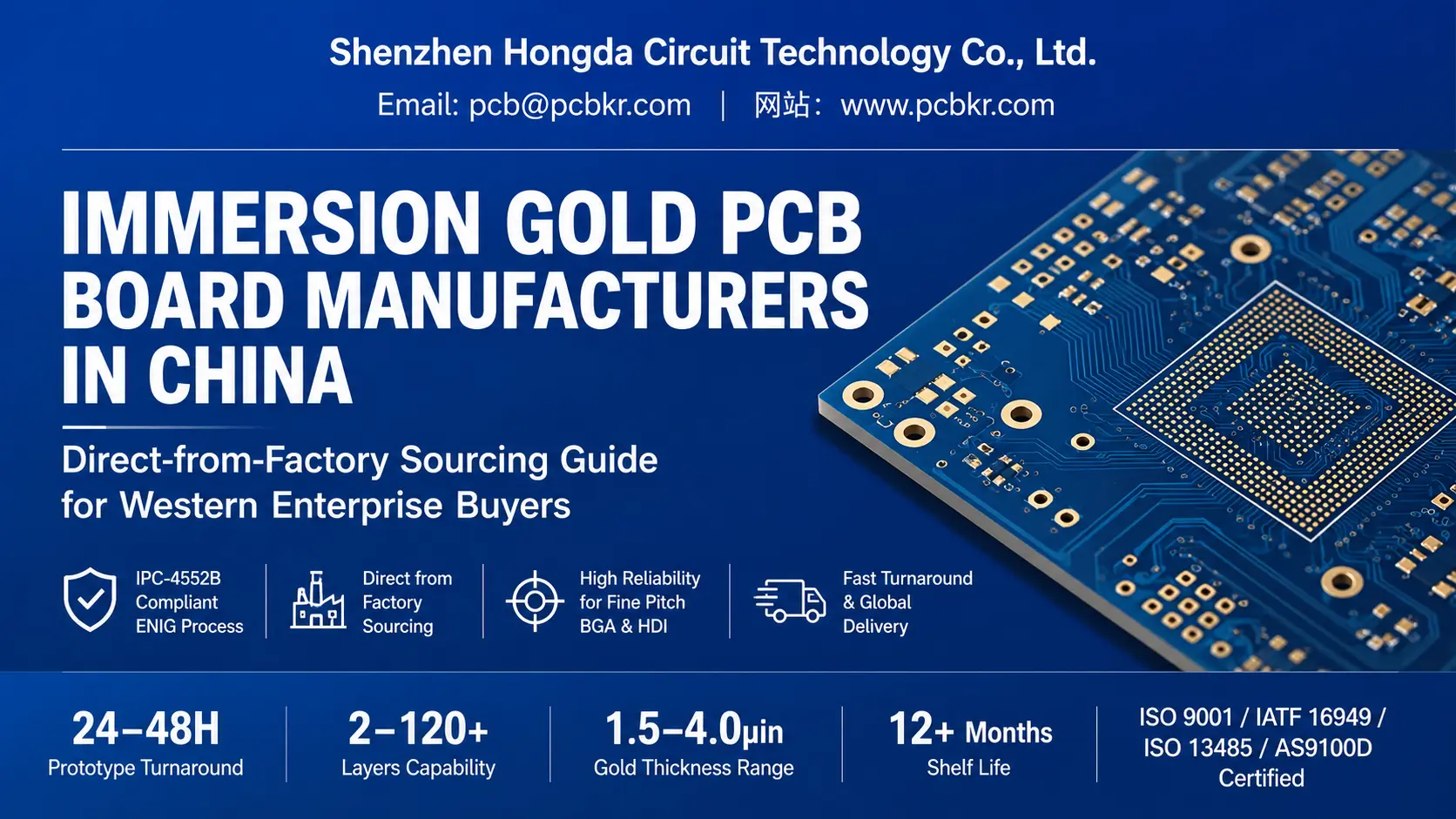
Immersion Gold PCB Board Manufacturers in China: Direct-from-Factory Sourcing Guide for Western Enterprise Buyers
Executive Summary: Standard ENIG Specifications at a Glance
For procurement engineers vetting immersion gold PCB board manufacturers in China, the first gate is verifying that the factory holds its electroless nickel immersion gold (ENIG) process within the IPC-4552B process window. The table below summarizes the non-negotiable parameters every Western buyer should demand on the fabrication drawing.
Table 1: ENIG specification matrix for direct-from-factory procurement. Values derived from IPC-4552B Amendment 1 and field-validated production data from Shenzhen Hongda Circuit Technology Co., Ltd.
| Parameter | IPC-4552B Target | Acceptable Window | Measurement Method |
|---|---|---|---|
| Gold Thickness | 2–4 µin (0.05–0.10 µm) | 1.2–5.0 µin | XRF, per panel |
| Nickel Thickness | 118–240 µin (3.0–6.0 µm) | 100–250 µin | XRF + cross-section |
| Phosphorus Content | 7–9 wt% | 7–10 wt% | Atomic absorption |
| Surface Flatness | <0.5 µm Ra | <1.0 µm Ra | Profilometer |
| Shelf Life (Vacuum Sealed) | 12+ months | 6–12 months | IPC J-STD-003 |
| Solderability | Wetting balance ≥90% | ≥85% | J-STD-003 wetting test |
Why Western Hardware OEMs Direct-Source Immersion Gold PCBs from China
Supply Chain Density and 30–45% Cost Efficiency Without Compromising IPC-Class 3
The decision to source ENIG-finished boards from electroless nickel immersion gold suppliers in China is no longer driven solely by unit cost. In 2026, the structural advantage lies in vertical integration density. Within a 50-kilometer radius of Shenzhen, a buyer can trace the entire value chain—from raw laminate (Panasonic Megtron, Isola I-Tera, Rogers RO4350B) through automated ENIG plating lines, precision laser drilling, and same-day courier consolidation for DHL/FedEx export.
This ecosystem delivers three procurement advantages that Western fabricators struggle to match:
- Material agility. When Megtron 6 lead times spiked to 14–18 weeks in Q3 2025, Chinese manufacturers with pre-qualified hybrid stack-up programs maintained continuous production by substituting Shengyi S1000-2 on power planes without redesigning signal layers. A domestic US shop would have forced a 12-week schedule slip.
- Process convergence. The same factories running 224G PAM4 AI server backplanes with ±25 µm interlayer alignment tolerance apply that precision discipline to conventional multilayer ENIG boards. Your standard 8-layer FR-4 board benefits from equipment over-capacity originally installed for semiconductor test substrates.
- Cost structure. Labor arbitrage has flattened, but capital efficiency has not. A Chinese factory amortizing its SCREEN Ledia LDI exposure system across 10,000 panels per week can price a 6-layer ENIG prototype at 30–45% below a European shop with identical IPC-6012 Class 3 certification.
NPI Prototype vs. Mass Production Lead Time Matrix
Table 2: Lead-time comparison for ENIG PCB procurement. China-direct sourcing with express logistics often beats domestic fabrication on total time-to-market for prototype and low-volume runs.
| Phase | Domestic Turnaround | China Direct (Hongda) | Shipping | Total Door-to-Door |
|---|---|---|---|---|
| NPI / Prototype (1–10 pcs) | 5–10 days | 24–48 hours fabrication | DHL Express 3-day | 4–6 days |
| Low-Volume (100–500 pcs) | 10–15 days | 5–7 days fabrication | Air freight 5-day | 10–12 days |
| High-Volume (5,000+ pcs) | 15–20 days | 7–14 days fabrication | Sea freight 18–25 day | 25–39 days |
The critical procurement insight: for NPI cycles where every day of delay burns runway, a 24-hour ENIG prototype turnaround from Shenzhen, coupled with 3-day DHL transit, frequently outperforms a domestic 7-day fab that queues your job behind automotive production lots.
2026 ENIG Technology Trends Reshaping Chinese Manufacturing

Automated ENIG Plating Line with AI-Driven Bath Monitoring in Shenzhen Smart PCB Manufacturing Facility
AI-Driven Process Control and Real-Time Bath Monitoring
The most significant shift in ENIG PCB surface finish production since 2024 is the migration from manual bath titration to closed-loop AI dosing. Leading Chinese factories—including Shenzhen Hongda Circuit Technology—now deploy automated atomic absorption spectroscopy linked to ERP systems that adjust nickel bath pH, temperature, and stabilizer concentration every 15 minutes.
What this means for procurement engineers:
• Phosphorus drift is caught before it breeds black pad. Instead of weekly bath analysis, real-time ionic monitoring triggers alerts when phosphorus content deviates beyond 8.5 wt%. The line pauses, chemistry is corrected, and the lot is released only after XRF re-verification.
• Gold thickness uniformity tightens. Automated immersion gold dwell-time control holds thickness within ±0.01 µm across a 24-inch panel, eliminating the edge-thick/center-thin variation that plagues manual lines.
• Traceability becomes granular. Every panel carries a QR code linking to its nickel bath MTO (metal turnover) count, gold bath pH log, and XRF measurement coordinates. When your incoming QC requests documentation, you receive data, not assurances.
Eco-Friendly Low-Toxicity ENIG Chemistry for RoHS-Compliant Export
European buyers face increasing pressure from the EU Green Deal and upcoming REACH amendments targeting nickel salts and cyanide-based gold baths. Chinese immersion gold PCB board manufacturers serving export markets have responded by qualifying water-based, low-toxicity ENIG chemistries from suppliers like MacDermid Alpha and Atotech.
These 2026-formulation baths reduce hazardous waste generation by 40% while maintaining the same solderability performance. For procurement teams at medical device OEMs bound by ISO 13485 and impending EU environmental audits, specifying a low-toxicity ENIG process is becoming a contractual requirement rather than a preference.
Ultra-Thin Gold Deposition for 224G PAM4 and High-Frequency Applications
At 56 GHz Nyquist frequencies, every nanometer of surface roughness matters. Traditional ENIG deposits at 3–4 µin (0.075–0.10 µm) introduce slight nodularity that elevates insertion loss on microstrip lines. The 2026 response from high-end Chinese factories is controlled-thin ENIG at 1.5–2.0 µin (0.04–0.05 µm)—still within the IPC-4552B Amendment 1 lower limit of 0.04 µm, but optimized for signal integrity.
Shenzhen Hongda Circuit Technology applies this ultra-thin ENIG protocol to its 224G PAM4 AI server backplanes and RF microwave boards, pairing it with ULP-RTF (ultra-low profile reverse-treated foil) copper to minimize conductor loss. The same process is available for standard multilayer boards when the procurement spec explicitly calls out “thin-ENIG, 1.5–2.0 µin, signal integrity application.”
IPC-4552B Technical Parameter Matrix — What Procurement Engineers Must Verify
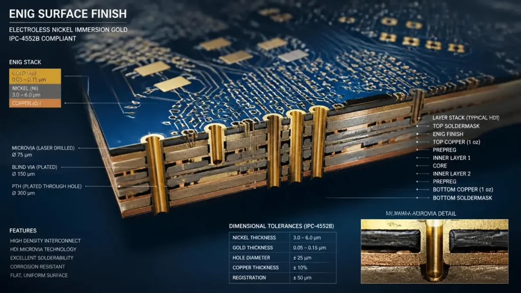
3D Cross-Section and Layer Stackup of IPC-4552B Compliant ENIG Surface Finish on HDI PCB
Gold and Nickel Thickness Windows Per IPC-4552B Amendment 1
IPC-4552B Amendment 1 (2024) refined the acceptable gold thickness window to 0.05–0.10 µm (2–4 µin), with a provision for AABUS (As Agreed Between User and Supplier) down to 0.04 µm for specialized high-frequency applications. The nickel underlayer must measure 3.0–6.0 µm (118–240 µin).
Procurement specification language to copy into your fab drawing:
“Surface Finish: Electroless Nickel Immersion Gold (ENIG) per IPC-4552B. Gold thickness: 0.05–0.10 µm, measured by XRF on actual pads (not breakaway coupons). Nickel thickness: 3.0–6.0 µm. Phosphorus content: 7–9 wt% per atomic absorption. Supplier shall provide batch XRF report and bath chemistry log with each shipment.”
Why specify measurement on actual pads? Breakaway coupons often plate at different current densities and can misrepresent the board’s true thickness by ±15%. A supplier measuring only coupons is cutting corners.
Phosphorus Content Control and Black Pad Prevention Thresholds
Black pad is not an urban legend. It is a hyper-corrosion phenomenon at the nickel-gold interface caused by aggressive gold replacement chemistry attacking phosphorus-rich grain boundaries. When phosphorus exceeds 10 wt%, the nickel layer becomes brittle and unsolderable. The defect is invisible to X-ray and often escapes AOI; it reveals itself only during thermal cycling or mechanical shock.
The three-layer defense every buyer should mandate:
- Bath chemistry control. Require weekly atomic absorption reports showing phosphorus at 7–9 wt%. Reject any batch where phosphorus exceeds 9.5 wt%.
- Immersion time gating. Gold bath dwell time must stay within ±10% of the qualified process window. Over-immersion is the fastest route to hyper-corrosion.
- Cross-sectional validation. On first article and annual requalification, demand SEM/EDS cross-sections on 5 pads per panel. The P-rich layer must not exceed 10% of total nickel thickness.
Shenzhen Hongda Circuit Technology maintains a dedicated ENIG process engineering team that logs every bath parameter to a cloud-based SPC system. Buyers receive a unique lot certificate with each shipment documenting nickel MTO count, gold bath pH, and XRF pad coordinates.
ENIG vs. ENEPIG vs. HASL — Surface Finish Selection Logic
Table 3: Surface finish selection matrix for procurement engineers. ENIG remains the default for fine-pitch SMT assemblies requiring 12+ month shelf life.
| Finish | Gold Thickness | Best For | Avoid When | Relative Cost |
|---|---|---|---|---|
| ENIG | 2–4 µin | Fine-pitch BGA, SMT, general high-reliability | Heavy wire bonding (Al) | 1.0× (baseline) |
| ENEPIG | 2–4 µin Au + 2–4 µin Pd | Wire bonding (Al & Au), press-fit, dual-use | Cost-sensitive consumer | 1.4–1.6× |
| HASL (Lead-Free) | N/A | Through-hole, large components, lowest cost | Pitch <0.5 mm, flatness critical | 0.6× |
| OSP | N/A | Single-reflow, cost-driven consumer | Multiple thermal cycles, long shelf life | 0.5× |
Decision rule: Switch from HASL to ENIG when your design includes components with pitch below 0.5 mm, requires multiple reflow cycles, or must survive 12+ months of warehouse storage before assembly. The flat coplanarity of ENIG (<0.5 µm Ra) prevents solder bridging on 0.4 mm pitch BGAs that HASL’s meniscus topography cannot support.
Shenzhen Hongda Circuit Technology Co., Ltd. — Factory Capability Profile
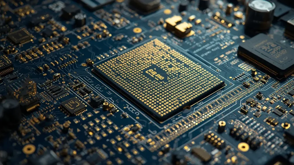
Ultra-flat Coplanar Immersion Gold (ENIG) Finish on High-Density BGA Array for Enterprise Server Backplane
Advanced ENIG Plating Line Equipment and XRF Metrology
Shenzhen Hongda Circuit Technology Co., Ltd. (trade name: PCBkr) operates a 2026-spec ENIG plating line in its Baoan, Shenzhen facility. The line is configured for both standard-thickness ENIG (2–4 µin gold) and thin-ENIG (1.5–2.0 µin) for high-frequency applications.
Key equipment on the ENIG line:
• SCREEN Ledia LDI Exposure Machine: Direct imaging for soldermask and etch resist, eliminating phototool degradation that can cause pad-size variation and subsequent plating non-uniformity.
• Mitsubishi UV/CO₂ Laser Drilling: Microvia formation down to 0.075 mm, ensuring pad flatness before nickel deposition.
• LAUFFER Lamination System: Controlled-pressure lamination that prevents resin smear on microvias, a prerequisite for uniform electroless nickel coverage.
• Nordson DAGE X-Ray Tester: 3D X-ray inspection for void detection in plated through-holes and microvias, performed before ENIG processing.
• XRF Spectrometers (Fischer or equivalent): Non-destructive gold and nickel thickness measurement with programmable collimators for pad-specific readings. Calibrated weekly to NIST-traceable standards.
• Automated Atomic Absorption Spectrophotometer: Real-time nickel bath phosphorus analysis with ±0.2 wt% accuracy.
The factory’s quality system is certified to ISO 9001:2026, AS9100D (Aerospace), IATF 16949 (Automotive), and IPC-6012 Class 3/3A. For medical device OEMs, ISO 13485 compliance is maintained on dedicated production lanes.
From 2-Layer Prototypes to 120+ Layer Backplanes with ENIG Finish
Hongda’s manufacturing envelope spans the full procurement spectrum:
• Prototype / NPI: 2–8 layer ENIG boards, 24–48 hour fabrication, no MOQ. Ideal for hardware startups validating fine-pitch BGA footprints.
• Mid-Volume: 10–20 layer boards with controlled impedance, 5–7 day turn. Common in industrial automation and telecom infrastructure.
• High-Complexity: 32–120+ layer backplanes, hybrid stack-ups (Megtron 7/8 + Shengyi S1000-2), heavy copper (up to 6 oz), all with ENIG or ENEPIG finish. Validated for 224G PAM4 signal integrity.
The critical differentiator: Hongda applies the same interlayer alignment tolerance (±25 µm) and differential impedance control (±5%) from its AI server lines to conventional multilayer ENIG boards. A 12-layer industrial control board fabricated on this equipment achieves chip-level precision without the chip-level price.
mSAP and Any-Layer HDI Integration with Immersion Gold
For designs requiring line/space below 50 µm, Hongda offers mSAP (modified semi-additive process) with ENIG finish. The mSAP process deposits a thin seed layer, photolithographically defines traces, and electroplates copper before flash-etching—achieving 10–15 µm line widths with superior edge definition.
When paired with ENIG, mSAP enables:
• Any-layer HDI routing with 0.4 mm pitch BGA fan-out on 8–20 layer builds.
• Ultra-fine trace impedance control for 112G/224G SerDes lanes.
• Reduced undercut compared to subtractive etching, yielding more consistent nickel deposition and lower black pad risk.
B2B Supplier Evaluation Checklist — Auditing Chinese ENIG Manufacturers
Critical Certifications Before PO Issuance
Before releasing a purchase order to any ENIG PCB board manufacturer in China, verify the following documentation:
☐ ISO 9001:2015 or 9001:2026 — Quality management system (mandatory baseline).
☐ IPC-6012 Class 2 or Class 3 — Product performance specification. Class 3 is non-negotiable for aerospace, medical, and automotive.
☐ IPC-4552 — ENIG process qualification certificate from an accredited lab.
☐ IATF 16949 — Required if the boards will touch automotive electronics.
☐ ISO 13485 — Mandatory for medical device PCB assemblies.
☐ UL 94V-0 — Flammability rating for the base laminate.
☐ AS9100D — Aerospace quality standard; indicates the factory can handle mission-critical traceability.
Red flag: A supplier claiming “IPC compliance” but unable to produce a third-party audit report from the last 12 months. Self-declared compliance is not compliance.
In-House Inspection Equipment and DFM Review Protocols
A factory’s capital equipment list reveals its true quality ceiling. During your audit (virtual or on-site), verify the presence of:
Table 4: Minimum in-house metrology requirements for ENIG PCB suppliers serving Western OEMs.
| Equipment | Purpose | Minimum Specification |
|---|---|---|
| XRF Spectrometer | Gold/nickel thickness | NIST-traceable, pad-specific measurement |
| Cross-Section Microscope | IMC verification, black pad detection | 500×–1000× metallographic |
| SEM/EDS | Phosphorus mapping, corrosion depth | 10,000×, EDS capability |
| 3D AOI | Post-ENIG surface defect detection | 5 µm resolution |
| Wetting Balance | Solderability per J-STD-003 | 0.1 µN sensitivity |
| Impedance Test Probe | Controlled impedance validation | TDR-based, ±2% accuracy |
DFM review protocol: Demand a pre-production DFM report before committing to prototype tooling. At Hongda, the DFM team checks for solder mask dam width (minimum 75 µm for ENIG pads), trace-to-pad spacing, and microvia placement that could create plating voids. This review is delivered within 1 hour of Gerber submission and prevents costly redesigns after first article.
Bath Chemistry Documentation and MTO Log Requirements
The single most effective black pad prevention measure is forcing your supplier to deliver process data with every lot. Your incoming QC gate should require:
- Batch-specific XRF report — Gold and nickel thickness on 5 pads minimum, with panel coordinates.
- Nickel bath MTO log — Metal turnover count since last bath make-up. Reject if MTO exceeds the supplier’s qualified limit (typically 4–6 MTO).
- Gold bath pH/temperature log — Time-stamped readings from the production shift.
- Phosphorus analysis report — Atomic absorption result dated within 7 days of your panel’s plating.
- Cross-section photomicrograph — First article only, showing IMC formation and absence of P-rich spikes.
Factories that resist providing these documents usually have something to hide. Treat bath chemistry transparency as a proxy for management discipline.
Cross-Border Logistics, Customs, and IP Protection
Incoterms and Express Delivery Windows
For direct from factory ENIG PCB sourcing, Incoterms selection directly impacts landed cost and risk allocation:
• DDP (Delivered Duty Paid): Supplier handles customs, duties, and last-mile delivery. Best for first-time buyers unfamiliar with China export documentation. Hongda offers DDP to US/EU with 3–5 day express transit.
• DAP (Delivered at Place): Supplier delivers to your designated warehouse; you clear customs. Suitable if you have a preferred customs broker.
• FOB (Free on Board): You control freight from the Shenzhen port. Cost-effective for sea-freight volume orders above 500 kg.
Practical lead time: For prototype quantities under 10 kg, DHL/FedEx/UPS express from Hongda’s Baoan facility to San Francisco or Frankfurt averages 72 hours door-to-door. For volume production, air freight adds 5–7 days; sea freight adds 18–25 days but reduces per-unit shipping cost by 60–70%.
HS Code 8534.00.00 and Certificate of Origin
ENIG PCBs fall under HS Code 8534.00.00 — “Printed circuits.” Correct classification is essential; misclassification triggers customs delays and penalty duties. Request that your supplier includes:
• Commercial invoice with detailed layer count, dimensions, and surface finish type.
• Packing list with net/gross weight and harmonized code.
• Certificate of Origin (COO) from the China Council for the Promotion of International Trade (CCPIT), required for preferential tariff treatment under applicable trade agreements.
For US buyers, be aware that Section 301 tariffs may apply depending on current trade policy. Hongda’s logistics team pre-structures invoices to maximize transparency and minimize customs friction.
Bilateral NDAs and Gerber File Security
Intellectual property protection remains the top concern for Western hardware leads sourcing from China. A generic NDA printed from a template is insufficient.
Minimum IP protection stack:
- Bilateral NDA enforceable under Chinese contract law (PRC Contract Law), with jurisdiction specified in Shenzhen or Hong Kong courts.
- Secure file transfer via encrypted server (SFTP/HTTPS) with access logging.
- Internal file isolation: Gerber files stored on air-gapped workstations within the CAM engineering department, not on general corporate network drives.
- No third-party CAM outsourcing: Confirm that DFM and panelization are performed in-house. Outsourced CAM is the most common IP leak vector.
- Data retention policy: Supplier deletes Gerber files 90 days after final shipment unless otherwise agreed.
At Shenzhen Hongda Circuit Technology, proprietary designs are processed on isolated workstations with USB port lockdown. The engineering team signs individual confidentiality addendums, and the company maintains cyber liability insurance covering IP breach incidents.
Frequently Asked Questions — ENIG PCB Procurement for US/EU Buyers
What is the ideal gold thickness for ENIG PCB assembly to prevent black pad?
Per IPC-4552B, the optimal gold thickness window is 2.0–4.0 micro-inches (0.05–0.10 µm) over a minimum nickel thickness of 118 micro-inches (3.0 µm). For high-frequency applications where signal loss is critical, AABUS provisions allow thinning to 1.5–2.0 µin (0.04–0.05 µm), but this requires XRF equipment capable of accurate sub-0.05 µm measurement and may limit shelf life. Exceeding 4.0 µin risks gold embrittlement in solder joints; below 2.0 µin without AABUS documentation risks nickel oxidation during storage. Always demand pad-specific XRF reports—never accept coupon-only measurements.
How do Chinese immersion gold PCB manufacturers handle prototype turnaround times for US/EU clients?
Leading Chinese factories operate dedicated fast-turn prototype lanes with 24/7 staffing. At Shenzhen Hongda Circuit Technology, standard ENIG prototypes (2–8 layers) ship within 24–48 hours of Gerber approval, utilizing express international courier (DHL/FedEx) for 3-day door-to-door delivery to North America and Europe. For complex HDI or rigid-flex prototypes, the timeline extends to 72–96 hours. The critical path is usually DFM review and stack-up confirmation, not fabrication. Submitting complete fabrication notes and impedance requirements with your initial RFQ eliminates 80% of schedule delays
What certifications should I verify before sourcing ENIG PCBs from China?
The certification stack depends on your end market, but the universal baseline is ISO 9001 + IPC-6012 Class 3 + IPC-4552 ENIG qualification. Add IATF 16949 for automotive, ISO 13485 for medical, AS9100D for aerospace, and UL 94V-0 for flammability. Do not accept self-declarations—request third-party audit certificates with expiration dates. For ENIG specifically, verify that the factory’s IPC-4552 qualification is current (within 24 months) and covers the exact nickel bath chemistry they use for your product family.
ENIG vs. HASL — when should I switch for fine-pitch BGA assemblies?
Switch from HASL to ENIG when your design includes component pitches below 0.5 mm, requires multiple reflow cycles, or demands a shelf life exceeding 6 months. HASL produces a meniscus-shaped solder coating with surface variation of ±1.5 µm, which causes solder bridging on 0.4 mm pitch BGAs and coplanarity failures during automated optical inspection. ENIG delivers a flat, planar surface (<0.5 µm Ra) with 12+ month oxidation resistance. The cost delta is typically 30–40% higher than HASL, but the yield improvement on fine-pitch assemblies usually pays back within the first production lot.
How do I audit a Chinese ENIG supplier’s plating line without traveling to Shenzhen?
Remote audits can be rigorous if structured correctly. Request the following in sequence:
1. Live video walkthrough of the ENIG line, including bath tanks, XRF station, and cross-section lab. Record the session.
2.Process documentation package: Bath chemistry logs from the last 30 days, XRF calibration certificates, and IPC-4552 qualification report.
3.Virtual first-article inspection: Have the supplier stream real-time cross-sectioning and SEM imaging of your actual panel.
4.Third-party verification: Engage an accredited testing lab (e.g., SGS, Intertek) in Shenzhen to perform unannounced spot checks on your production lot.
5. Reference checks: Contact two Western OEMs currently in production with the supplier. Ask specifically about black pad incidence and documentation responsiveness.
If a supplier refuses any of these five steps, remove them from your AVL (approved vendor list). Transparency is not optional when solder joint reliability is on the line.
Fast-Track RFQ: Get Your ENIG Project Moving
Shenzhen Hongda Circuit Technology Co., Ltd. provides 24-hour DFM feedback and sample prototype evaluation for Western procurement teams. Submit your Gerber files, stack-up requirements, and target impedance profiles to sales@pcbkr.com for:
• Complimentary DFM review with solder mask dam and trace spacing optimization.
• Pad-specific XRF thickness guarantee per IPC-4552B.
• 24–48 hour prototype turnaround with DDP express delivery.
• Full bath chemistry documentation and lot traceability.
Direct Contact:
📧 sales@pcbkr.com
📧 pcb@pcbkr.com
📞 +86 0755 23720053
📍 Room 1608-1610, Research Development Comprehensive Building, Baoyunda Logistics Center, Baoan, Shenzhen, China
🏢 Unified Social Credit Code: 91440300MA5F6CA091
This sourcing guide was prepared by the engineering team at Shenzhen Hongda Circuit Technology Co., Ltd. and reflects production data validated through Q3 2026. For technical clarifications or custom ENIG specifications, contact our application engineering division.
About Author
David Chen https://www.linkedin.com/in/pcbcoming
David Chen boasts an extensive professional background in PCBA manufacturing, PCBA testing, and PCBA optimization, with specialized expertise in high-precision PCBA fault analysis and rigorous PCBA reliability testing. The author has worked with high-layer-count server PCB fabrication, ultra-low-loss backplane stackups, and thermo-mechanical reliability optimization for AI infrastructure projects involving 112G and 224G PAM4 architectures. Skilled in complex circuit design and cutting-edge advanced PCB manufacturing processes, he delivers solutions that elevate product durability and performance across industrial applications. His technical articles focusing on PCBA manufacturing workflows and testing methodologies are widely cited by industry peers, research institutions, and technical platforms, solidifying his reputation as a recognized technical authority in the global circuit board manufacturing sector.