PTFE PCB Material Procurement Guide: How to Select High-Frequency Teflon Laminates for 5G, RF & mmWave Applications
When your design crosses 10 GHz, standard FR‑4 stops being an option. The signal loss, impedance drift, and thermal instability of epoxy‑based substrates will degrade performance before the first prototype leaves the bench. That is the exact point where procurement teams and RF engineers start searching for PTFE PCB material—also widely known as Teflon PCB material—to maintain signal integrity in high‑frequency environments.
At Shenzhen Hongda Circuit Technology Co., Ltd., we fabricate PTFE‑based laminates daily for 5G base stations, satellite communication systems, and AI server backplanes. This guide is written specifically for buyers, sourcing managers, and RF design engineers who need to navigate the PTFE PCB procurement decision chain without overpaying for unnecessary performance or underestimating manufacturing complexity.
What Is PTFE PCB Material? A Procurement Primer on Teflon‑Based Laminates
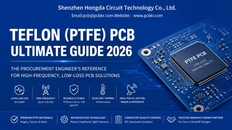
Before issuing an RFQ, you need to understand what you are actually buying. PTFE (polytetrafluoroethylene) is a fluoropolymer resin that delivers the lowest dielectric loss of any commercially available PCB substrate. In the supply chain, the terms PTFE PCB material and Teflon PCB material are used interchangeably—Teflon is simply the Chemours brand name for PTFE resin. For procurement purposes, both refer to the same material class: non‑polar, thermally stable, and chemically inert substrates ideal for microwave and millimeter‑wave applications.
A PTFE laminate PCB is not a single material specification. It is a family of substrates that ranges from pure PTFE (Dk ~2.1) to ceramic‑filled PTFE composites (Dk 2.5–10.2) and glass‑reinforced PTFE hybrids. Each variant serves a different frequency band, power level, and cost target. Rogers RO3003, Taconic TLY‑5, and Arlon AD series are common trade names you will encounter; however, the underlying chemistry is PTFE‑based, and the fabrication challenges remain consistent across suppliers.
The critical distinction for buyers is this: PTFE PCB material is a low‑loss PCB material by definition, but not all PTFE laminates are created equal. Dk tolerance, filler composition, and copper foil bonding strength vary by grade, and these variations directly impact yield, impedance control, and final unit cost.
Why PTFE Dominates High‑Frequency PCB Applications
If you are sourcing low‑loss PCB material for RF front‑ends, radar modules, or 800G optical interconnects, PTFE is not a luxury—it is a physical necessity. Here is why procurement teams specify it over FR‑4 once operating frequencies exceed 6 GHz.
Low Dielectric Constant (Dk) and Ultra‑Low Dissipation Factor (Df)
The two numbers that dominate every material datasheet are Dk (dielectric constant) and Df (dissipation factor, also called loss tangent).
- Dk determines signal propagation speed and trace geometry. PTFE materials offer Dk values between 2.1 and 3.5, significantly lower than FR‑4’s 4.2–4.8. Lower Dk means faster signal travel and tighter impedance control—essential for mmWave antenna arrays and high‑speed SerDes channels.
- Df quantifies how much signal energy converts to heat within the substrate. Standard FR‑4 shows Df of 0.015–0.025 at 10 GHz, which is acceptable for sub‑5 GHz designs but catastrophic at 28 GHz or 77 GHz radar bands. PTFE materials deliver Df as low as 0.0009–0.002, reducing insertion loss by an order of magnitude.
For buyers, this translates to a simple procurement rule: if your application operates above 10 GHz or requires long trace runs with minimal attenuation, PTFE is the only viable low‑loss PCB material in the standard laminate catalog.
Thermal Stability and Moisture Resistance
PTFE maintains its Dk and Df characteristics across temperature swings from ‑200°C to +260°C. Unlike FR‑4, which experiences glass‑transition degradation above 170°C, PTFE does not have a true Tg in the conventional sense. It also absorbs virtually no moisture—typically <0.02%—which prevents the Dk drift that plagues epoxy systems in humid or outdoor environments. For procurement teams qualifying suppliers for 5G outdoor base stations or aerospace applications, this environmental stability eliminates field‑failure risks that standard materials cannot address.
PTFE vs FR‑4 PCB Material: A Procurement Decision Matrix
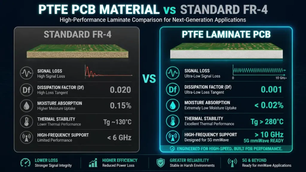
Performance and technical specification comparison between PTFE PCB material and standard FR-4 laminates.
Every RF project starts with the same question: Can we get away with FR‑4, or do we need PTFE? The answer depends on frequency, loss budget, environmental exposure, and—critically—total cost of ownership. Here is how the two materials compare across the metrics that actually drive purchasing decisions.
Dk and Df Comparison
| Parameter | Standard FR‑4 | PTFE Laminate PCB | Procurement Impact |
|---|---|---|---|
| Dk @ 10 GHz | 4.2 – 4.8 | 2.1 – 3.5 | PTFE enables smaller RF structures and tighter impedance tolerances |
| Df @ 10 GHz | 0.015 – 0.025 | 0.0009 – 0.002 | PTFE reduces signal loss by 5–10×, extending transmission distance |
| Dk Stability vs. Temp | Moderate drift | < ±0.02% | PTFE eliminates temperature‑induced phase errors |
| Moisture Absorption | 0.10 – 0.20% | < 0.02% | PTFE maintains performance in uncontrolled environments |
Manufacturing Complexity and Supplier Capability
FR‑4 processes on virtually any PCB line. PTFE does not. The non‑polar surface of PTFE resists chemical adhesion, requiring specialized surface preparation—typically plasma treatment or sodium‑naphthalene etching—before through‑hole plating. Drill parameters must be adjusted to accommodate the softer substrate, and lamination cycles require precise temperature and pressure control to prevent delamination.
For buyers, this means supplier qualification is non‑negotiable. A fabricator with standard FR‑4 capabilities cannot simply “run PTFE” without process validation, dedicated equipment, and trained technicians. At Shenzhen Hongda Circuit Technology, our PTFE production line operates independently from our FR‑4 facility, with dedicated plasma desmear chambers, low‑profile copper foil bonding processes, and impedance test coupons on every panel.
Total Cost of Ownership (TCO)
PTFE raw laminate costs 3× to 8× more than FR‑4 per square meter. However, TCO analysis often favors PTFE in high‑frequency applications because:
- Higher first‑pass yield reduces scrap and rework
- Lower insertion loss eliminates the need for external amplifiers
- Thermal stability reduces field‑failure warranty claims
The procurement sweet spot: Hybrid stack‑ups. Many 5G and radar designs use PTFE cores for critical signal layers and FR‑4 for power/ground layers. This approach cuts material costs by 30–50% while preserving RF performance on the traces that matter.
Shenzhen Hongda Circuit Technology: Advanced PTFE PCB Manufacturing Capabilities
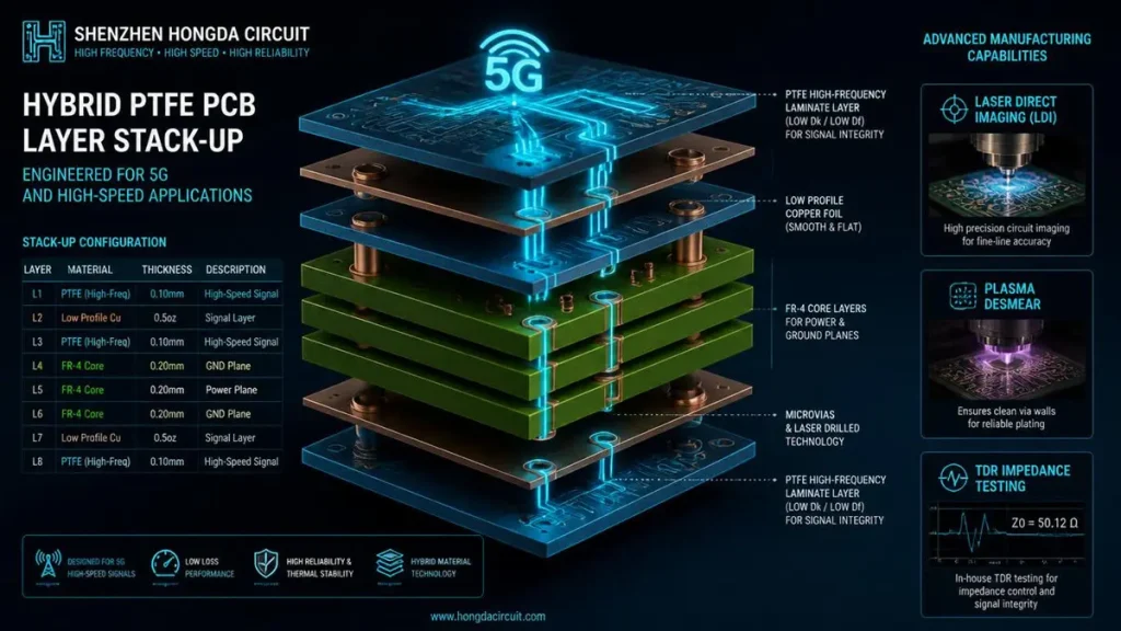
3D exploded view of an 8-layer hybrid PTFE/FR-4 PCB stack-up featuring Shenzhen Hongda Circuit’s advanced manufacturing capabilities (LDI, Plasma Desmear, and TDR Impedance Testing).
Selecting the right PTFE PCB supplier is as important as selecting the right material grade. Shenzhen Hongda Circuit Technology Co., Ltd. has invested in dedicated high‑frequency fabrication infrastructure to bridge the gap between material science and manufacturability.
Precision Fabrication Equipment for Low‑Loss PTFE Laminates
Our facility in Shenzhen operates a segregated clean‑room line for PTFE and ceramic‑filled RF substrates. Key capabilities include:
- Laser Direct Imaging (LDI): Achieves ±8 µm trace alignment accuracy on PTFE surfaces, critical for 77 GHz automotive radar and mmWave 5G antenna designs where 50‑ohm tolerances must hold within ±5%.
- Plasma Desmear & Sodium Etch Systems: Dual‑surface preparation protocols ensure copper peel strength >1.2 N/mm on PTFE substrates, eliminating the via pullout and plating void issues that plague inexperienced fabricators.
- Controlled‑Depth Laser Drilling: Enables blind and buried vias in hybrid PTFE/FR‑4 stack‑ups with ±10 µm depth control, supporting 12‑layer to 40‑layer high‑speed backplanes for AI server applications.
- Automated Impedance Testing: Every production panel includes TDR (Time Domain Reflectometry) test coupons verified against customer simulation models. Data is archived per IPC‑6012 Class 3 requirements.
Hybrid Stack‑Up Engineering for Cost‑Optimized RF Designs
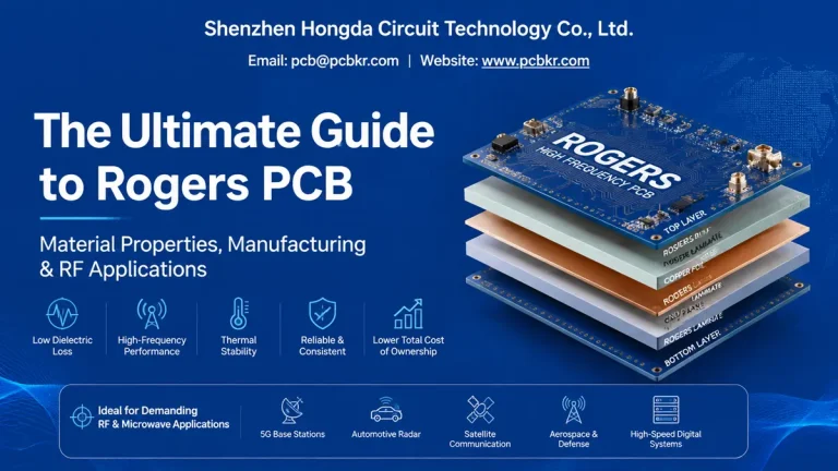
Not every layer needs PTFE. Our engineering team specializes in hybrid constructions that place PTFE cores (Rogers RO3003, Taconic TLY‑5, or equivalent) on outer signal layers while using standard FR‑4 or mid‑loss PPO materials for internal power planes. This approach is now standard for 5G massive MIMO antennas and 112Gbps PAM4 backplanes, where it delivers PTFE‑like signal integrity at 40% lower material cost.
Quality Certification and Supply Chain Resilience
We maintain ISO 9001, ISO 14001, and IPC‑A‑610 Class 3 certifications. For aerospace and defense buyers, our lot‑traceability system tracks every sheet of laminate from raw material receipt through final electrical test. In 2026, with high‑performance copper foil and low‑Dk CCL supply chains under constraint, our direct partnerships with Rogers, Taconic, and Shengyi ensure allocated material stock for volume orders—reducing lead‑time risk for procurement teams.
The PTFE PCB Procurement Decision Chain: A 5‑Step Sourcing Framework
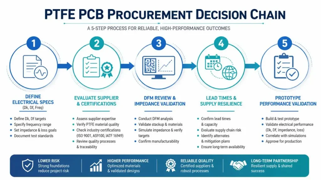
The 5-step sourcing framework for procuring high-frequency PTFE PCB materials to ensure zero-defect quality and supply chain resilience.
Procurement managers in the RF and telecom sectors follow a predictable decision chain when qualifying PTFE PCB manufacturers. Align your sourcing process with these five steps to eliminate supplier risk and lock in performance guarantees.
Step 1 – Define Electrical Requirements: Dk, Df, and Frequency Range
Before contacting suppliers, lock down your electrical specification:
- Operating frequency band: Sub‑6 GHz, 28 GHz mmWave, or 77–81 GHz radar?
- Loss budget: How much insertion loss can your link tolerate over the longest trace?
- Impedance targets: 50‑ohm single‑ended, 100‑ohm differential, or coplanar waveguide?
Use these parameters to filter the high‑speed PCB Dk Df database and narrow your material grade. For example, 28 GHz 5G base station antennas typically require Df < 0.002 and Dk stability across ‑40°C to +85°C—specifications that point directly to ceramic‑filled PTFE or ultra‑low‑loss hydrocarbon alternatives.
Step 2 – Evaluate Supplier Manufacturing Capabilities and Material Certifications
Send your preliminary stack‑up to three qualified fabricators and ask specific questions:
- Do you operate a dedicated PTFE production line, or do you process PTFE on shared FR‑4 equipment? (Shared lines risk cross‑contamination and adhesion failures.)
- What is your validated copper peel strength on PTFE after thermal cycling?
- Can you provide IPC‑TM‑650 Method 2.5.5.5 Dk/Df test data at my operating frequency?
At Shenzhen Hongda Circuit Technology, we provide batch‑specific Dk/Df validation reports and welcome customer witness audits of our plasma treatment and impedance testing stations.
Step 3 – Request DFM Review and Impedance Simulation Validation
A capable PTFE PCB manufacturer will not simply accept your Gerbers. They will perform a Design for Manufacturability (DFM) review focused on:
- Trace width vs. dielectric thickness feasibility
- Via aspect ratio limits in soft PTFE cores
- Thermal management for high‑power RF amplifiers
- Hybrid layer registration tolerances
We use Polar SI9000e and HyperLynx field solvers to validate stack‑up impedance before CAM processing. This step catches 90% of signal integrity issues before the first panel is laminated.
Step 4 – Assess Lead Times, MOQ, and Supply Chain Resilience
PTFE laminate lead times in 2026 range from 4 to 12 weeks depending on grade and global demand. Ask your supplier:
- Do they hold safety stock of Rogers/Taconic materials?
- What is their typical MOQ for prototype vs. production?
- Can they support consigned material if you have direct laminate contracts?
Our standard lead time for 2–4 layer PTFE prototypes is 7–10 days; volume orders with allocated material run 3–4 weeks. For critical telecom infrastructure projects, we offer bonded inventory programs that guarantee 2‑week turnaround for 12 months.
Step 5 – Validate Prototype Performance Before Volume Commitment
Never skip the prototype qualification phase. Require your supplier to deliver:
- TDR impedance plots across the full panel
- S‑parameter measurements (if in‑house RF test is available)
- Cross‑sectional micrographs showing copper‑to‑PTFE adhesion and via barrel quality
- Thermal cycle data (if applicable to your environmental spec)
Only after prototype validation meets your simulation correlation should you release production volumes. This discipline protects procurement teams from the catastrophic cost of discovering impedance mismatches at 10,000 units.
2026 PCB Manufacturing Trends Impacting PTFE Material Procurement
The high‑frequency PCB market is shifting rapidly. Three trends directly affect how buyers source PTFE laminates this year.
AI Server and 800G Optical Interconnect Demand Driving Substrate Shortages
AI infrastructure deployment is accelerating demand for ultra‑low‑loss materials across both digital and RF domains. NVIDIA Rubin‑class servers and 800G/1.6T optical transceivers require backplanes with Df < 0.002 and layer counts exceeding 30 layers. This demand is consuming PTFE and advanced hydrocarbon laminate capacity, extending lead times and increasing price volatility. Procurement teams should lock in annual supply agreements rather than relying on spot purchases.
Advanced Laser Drilling and Plasma Treatment for PTFE Via Reliability
Newer PTFE fabrication facilities are adopting UV laser drilling with <20 µm spot size to create microvias in ceramic‑filled PTFE without substrate tearing. Combined with in‑line plasma treatment systems, these advances are pushing PTFE reliability into FR‑4 territory—opening the door for PTFE use in HDI applications previously considered impossible.
Generative AI in PCB Design and Predictive Quality Control
Leading fabricators are now using machine‑learning models trained on historical Dk/Df variation data to predict stack‑up performance before lamination. For buyers, this means tighter impedance distributions, fewer yield excursions, and faster qualification cycles. At Shenzhen Hongda Circuit Technology, we have integrated AI‑driven defect detection into our AOI process for PTFE panels, reducing escape rates by 40% compared to rule‑based inspection.
PTFE PCB Material Keyword Matrix for SEO & Content Strategy
For marketing teams building topical authority around Teflon PCB material and low‑loss PCB substrate topics, we recommend this three‑tier keyword architecture:
| Tier | Keyword Category | Target Keywords & Phrases |
|---|---|---|
| Tier 1 – Core Keywords (High volume, high competition) | Primary material terms | PTFE PCB material, Teflon PCB material, Low loss PCB material, High frequency PCB, RF PCB substrate |
| Tier 2 – Derivative & Variant Keywords (Mid‑volume, purchase intent) | Application & comparison terms | PTFE laminate PCB, PTFE vs FR4 PCB, Ceramic filled PTFE, Microwave PCB material, Ultra low loss substrate, Rogers RO3003 alternative, High speed PCB material selection |
| Tier 3 – Long‑Tail Keywords (Low volume, high conversion) | Procurement & specific use cases | PTFE PCB material for 5G base station, Best PTFE PCB material for mmWave antenna, PTFE PCB procurement guide for RF engineers, Low Dk low Df PTFE laminate supplier China, Teflon PCB vs Rogers RO3003 comparison, High frequency PTFE PCB manufacturing capabilities, PTFE hybrid stack up cost optimization, PTFE PCB material Dk Df specifications buyer guide |
Content deployment recommendation: Use Tier 1 keywords in H1 and title tags; Tier 2 keywords in H2 headings and anchor text; Tier 3 keywords in FAQ schema, image alt text, and supporting blog posts.
Frequently Asked Questions (FAQ) – What Procurement Managers Ask When Sourcing PTFE PCB Suppliers
How do I verify that a PTFE PCB manufacturer can actually process Teflon laminates, not just FR‑4?
Request documentation of their dedicated PTFE production line, including plasma treatment or sodium‑etch equipment, and ask for peel strength test data on PTFE‑to‑copper bonds. A qualified supplier should also provide cross‑sectional micrographs of PTFE vias and TDR impedance reports from recent production lots. At Shenzhen Hongda Circuit Technology, we welcome virtual or on‑site audits of our PTFE fabrication cell.
What is the real lead time for PTFE PCB prototypes vs. production volumes in 2026?
Prototype lead times for 2–4 layer PTFE designs typically range from 7 to 15 days at qualified facilities. Production volumes depend heavily on material allocation; standard grades like Rogers RO4350B or RO3003 may ship in 3–4 weeks, while specialized ceramic‑filled PTFE can extend to 8–12 weeks due to AI server demand. We recommend bonding inventory agreements for projects requiring guaranteed 4‑week turnaround.
Is PTFE always better than FR‑4 for high‑frequency designs, or are there exceptions?
PTFE is mandatory above 10 GHz and for applications with strict loss budgets. However, for sub‑6 GHz designs with moderate performance requirements, high‑quality FR‑4 or mid‑loss PPO materials (e.g., Shengyi S7136, Isola FR408HR) offer adequate performance at significantly lower cost. The optimal approach is often a hybrid PTFE/FR‑4 stack‑up, using PTFE only on signal layers that require it.
How does moisture absorption affect PTFE PCB performance in outdoor 5G or marine applications?
PTFE absorbs <0.02% moisture, compared to 0.10–0.20% for standard FR‑4. Near‑zero moisture uptake prevents the Dk shift and insertion loss degradation that cause antenna detuning in humid environments. For procurement teams specifying outdoor infrastructure, PTFE’s moisture immunity is a primary reliability factor that justifies its higher material cost.
What certifications and quality standards should I demand from a PTFE PCB supplier for aerospace or defense programs?
Minimum requirements include ISO 9001, IPC‑A‑610 Class 3, and IPC‑6012 Class 3. For military or space applications, ask for MIL‑PRF‑55110 or AS9100 certification, plus full lot traceability from raw laminate to finished PCB. Impedance validation should follow IPC‑TM‑650 test methods, and the supplier must maintain segregated work‑in‑process tracking for PTFE jobs to prevent material cross‑contamination.
Ready to source PTFE PCB material for your next high‑frequency project?
Contact Shenzhen Hongda Circuit Technology Co., Ltd. for a free DFM review, stack‑up optimization, and competitive quotation. Visit www.pcbkr.com or email our RF engineering team directly.
About Author
David Chen https://www.linkedin.com/in/pcbcoming
David Chen boasts an extensive professional background in PCBA manufacturing, PCBA testing, and PCBA optimization, with specialized expertise in high-precision PCBA fault analysis and rigorous PCBA reliability testing. The author has worked with high-layer-count server PCB fabrication, ultra-low-loss backplane stackups, and thermo-mechanical reliability optimization for AI infrastructure projects involving 112G and 224G PAM4 architectures. Skilled in complex circuit design and cutting-edge advanced PCB manufacturing processes, he delivers solutions that elevate product durability and performance across industrial applications. His technical articles focusing on PCBA manufacturing workflows and testing methodologies are widely cited by industry peers, research institutions, and technical platforms, solidifying his reputation as a recognized technical authority in the global circuit board manufacturing sector.