Teflon PCB Manufacturer: Complete Guide to PTFE High Frequency PCB Manufacturing
Teflon PCB—more precisely PTFE PCB—represents the upper tier of high-frequency substrate technology. When your design crosses into millimeter-wave territory, standard FR-4 ceases to be an option and becomes a liability. The dielectric loss factor (Df) of FR-4 hovers around 0.0200; PTFE laminates such as Rogers RT5880 push that figure down to 0.0009. That is not an incremental improvement. It is a twenty-fold reduction in signal attenuation, and it explains why aerospace contractors, 5G infrastructure OEMs, and automotive radar developers specify Teflon PCB boards for mission-critical RF layers.
This guide is written for procurement engineers and hardware program managers who need more than a generic material overview. You need a decision framework: when to specify PTFE over hydrocarbon Rogers, how to validate a supplier’s plasma treatment capability, what drives Teflon PCB cost, and how to structure an RFQ that returns comparable quotes. We have organized the content around the actual purchasing workflow—material selection, process verification, application matching, supplier qualification, and quote negotiation—so you can use this as a working reference rather than passive reading.
What Is Teflon PCB? Understanding PTFE PCB Material and Construction
A Teflon PCB is a printed circuit board fabricated using polytetrafluoroethylene (PTFE) resin systems, often reinforced with woven glass fiber or ceramic fillers to improve mechanical stability and dimensional tolerance. The term “Teflon” is Chemours’ brand name for PTFE, but in the PCB industry it has become shorthand for any fluoropolymer-based high-frequency laminate, including Rogers RT/duroid series, Taconic TLY and TLP families, and Shengyi S7439.
Unlike standard epoxy-based FR-4, PTFE PCB material relies on carbon-fluorine molecular bonds that exhibit extremely low polarizability. This molecular structure is what delivers the ultra-low dissipation factor and near-constant dielectric constant (Dk) across multi-gigahertz frequency ranges.
PTFE PCB vs. Standard FR4: Why Dielectric Loss Matters
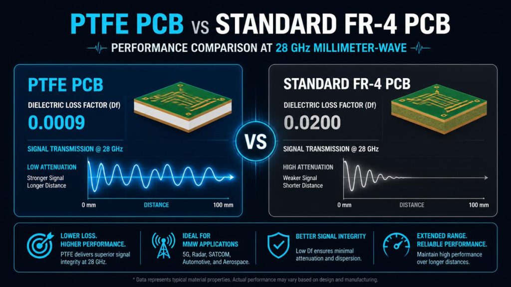
Performance & Dielectric Loss Comparison (PTFE vs. Standard FR-4 at 28 GHz)
At 28 GHz—the center frequency for many 5G mmWave deployments—insertion loss is dominated by dielectric attenuation. FR-4’s Df of 0.0200 translates to roughly 0.8 dB/cm of loss on a 50-ohm microstrip trace. Rogers RT5880, with Df 0.0009, cuts that to approximately 0.04 dB/cm. For a base station antenna feed network spanning 15 cm, the cumulative difference exceeds 11 dB. That is the margin between a functional link budget and a failed field trial.
The implication for procurement is straightforward: if your program operates above 10 GHz, or if phase consistency across a large antenna array is non-negotiable, PTFE becomes a material requirement rather than a premium option.
Common Teflon PCB Material Grades: Rogers RT5880, RT5870, and Taconic TLY-5
Not all PTFE laminates are identical. Material selection must balance electrical performance, thermal coefficient of dielectric constant (TCDk), and manufacturability:
| Material | Dk @10 GHz | Df @10 GHz | TCDk (ppm/°C) | Best Fit Application |
|---|---|---|---|---|
| Rogers RT5880 | 2.20 ± 0.02 | 0.0009 | -125 | Satellite communications, wideband EW, W-band radar |
| Rogers RT5870 | 2.33 ± 0.02 | 0.0012 | -115 | Aerospace RF modules, precision test fixtures |
| Taconic TLY-5 | 2.20 | 0.0009 | -130 | 5G antenna arrays, low-PIM base station filters |
| Rogers RO3003 | 3.00 ± 0.04 | 0.0010 | -3 | 77 GHz automotive radar, mmWave phased arrays |
For most 5G sub-6 GHz and mid-band applications, Rogers RO4350B (hydrocarbon-ceramic, Df 0.0037) provides adequate performance at lower material cost. The shift to pure PTFE is justified when frequencies exceed 20 GHz, or when the loss budget is constrained by regulatory emission limits or battery-powered transmitters.
Why Choose PTFE Material for High Frequency PCB and RF Applications?
The decision to specify a high frequency Teflon PCB extends beyond raw insertion loss numbers. PTFE laminates offer a combination of properties that address the full environmental and electrical stress profile of advanced RF hardware.
Low Loss PCB Performance: Df 0.0009 and Signal Integrity at mmWave
At mmWave frequencies, skin effect losses in copper traces and dielectric losses in the substrate are the two dominant attenuation mechanisms. While ultra-low-profile (ULP) copper foils address the former, only material selection fixes the latter. PTFE’s Df of 0.0009—approaching the theoretical limit for organic laminates—enables:
- Longer feed networks on phased-array antennas without excessive cumulative loss
- Higher Q-factor resonators for compact filter and oscillator designs
- Tighter phase tolerances across temperature swings, critical for beam-steering accuracy in 5G massive MIMO systems
For procurement teams evaluating Teflon PCB board suppliers, request documented Df and Dk values measured at your specific operating frequency, not just the datasheet headline at 10 GHz. Dk can drift by 0.05 or more between 10 GHz and 77 GHz on some ceramic-filled grades.
Thermal Stability and Moisture Resistance in Harsh Environments
PTFE laminates absorb less than 0.02% moisture by weight. In humid climates or sealed outdoor enclosures, this prevents the Dk shifts and impedance drift that plague standard materials. Additionally, PTFE’s extremely low coefficient of thermal expansion in the Z-axis (typically 180–280 ppm/°C, depending on filler loading) reduces the risk of via barrel cracking during thermal cycling.
For aerospace and defense programs, this translates to qualification test compliance. A Teflon PCB material stackup that survives 500 thermal cycles from -55°C to +125°C without delamination or resistance shift is not exceptional—it is the baseline expectation for IPC-6012 Class 3A builds.
Teflon PCB Manufacturing Process: How PTFE PCB Fabrication Differs from Standard Boards
PTFE PCB fabrication is not FR-4 processing with a different laminate. The chemical inertness of fluoropolymer resins introduces specific challenges that separate capable high frequency PCB manufacturers from commodity fabricators. If your supplier treats PTFE like ordinary substrate, you will see plating voids, delamination, and impedance failures.
Plasma Activation and Sodium Naphthalene Etching for Copper Adhesion
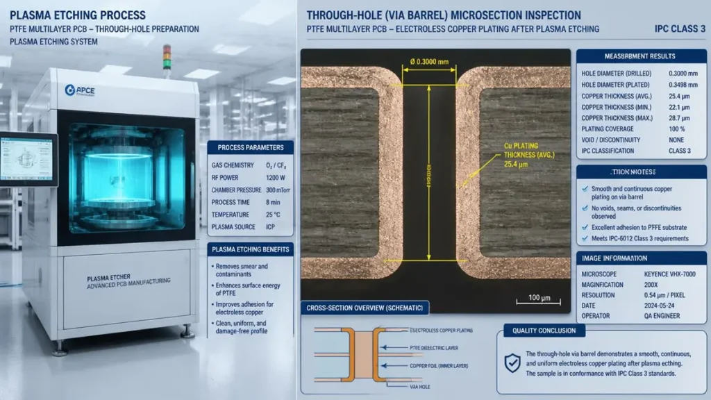
In-house plasma etching process (left) and cross-section inspection report of PTFE via barrel showing continuous copper adhesion meeting IPC Class 3 standards (right).
PTFE’s surface energy is approximately 18 dynes/cm—roughly one-third that of FR-4. Electroless copper will not adhere to untreated PTFE hole walls. Before through-hole plating, the fabricator must activate the surface through one of two methods:
- Plasma etching using a tetrafluoromethane/oxygen mixture to roughen the hole wall and introduce functional groups for copper nucleation
- Sodium naphthalene chemical etching, which defluorinates the surface to create a carbonaceous layer with improved wetting characteristics
Plasma treatment is the preferred method for multilayer PTFE PCB boards because it offers better process control and avoids the hazardous waste management associated with sodium chemistry. At Shenzhen Hongda Circuit Technology, all PTFE-based builds undergo in-house plasma activation prior to electroless copper deposition, with cross-section verification on first-article inspection reports.
Controlled Lamination Above 350°C and Specialized Drill Parameters
Standard FR-4 laminates press at 180–200°C. PTFE materials require lamination temperatures exceeding 350°C to achieve proper resin flow and bonding, which demands high-temp press platens and specialized bondplies. Over-pressurization causes resin squeeze-out and dielectric thickness variation; under-pressurization yields voids and poor interlaminar adhesion.
Drilling parameters also differ. PTFE’s soft, fibrous structure smears at high spindle speeds and tears at low feed rates. High-helix drill geometries with controlled entry/exit boards are required to achieve clean hole walls. For high-aspect-ratio vias in multilayer Teflon PCB builds, fabricators must optimize chip load and peck depth to prevent barrel roughness that would compromise impedance control.
Hybrid Stackup Design: Combining PTFE Cores with FR4 for Cost Optimization
A full PTFE multilayer can cost four to eight times an equivalent FR-4 board. For many programs, a hybrid stackup provides the optimal compromise: PTFE cores on RF signal layers, with standard FR-4 or low-loss PPE prepreg for power and digital routing layers. This approach can reduce material cost by 40–60% while preserving low-loss performance on critical traces.
However, hybrid Teflon PCB stackups introduce CTE mismatch risks. The procurement team should verify that the fabricator has qualified specific FR-4 prepreg combinations with their PTFE cores and can provide thermal cycle reliability data for the exact layer count and thickness under consideration.
Teflon PCB Applications: From 5G Antenna Arrays to Aerospace Radar Systems
The commercial demand for custom Teflon PCB solutions is not theoretical. It is being driven by specific, high-growth end markets with unforgiving electrical requirements.
5G Base Station and mmWave Antenna PCB Requirements
Massive MIMO antenna arrays operating at 28 GHz and 39 GHz require phase-matched feed networks across panels that may exceed 400 mm in length. PTFE’s stable Dk and ultra-low Df ensure that the phase relationship between antenna element A and element Z remains within the ±5° tolerance required for accurate beam steering. Base station OEMs commonly specify Rogers RO3003 or Taconic TLY-5 for these layers, with rolled copper to minimize passive intermodulation (PIM) below -160 dBc.
77 GHz Automotive Radar and ADAS Sensor Modules
Automotive radar at 77–81 GHz demands consistent dielectric performance across the -40°C to +125°C automotive temperature range. PTFE laminates with near-zero TCDk, such as RO3003, prevent frequency drift that would degrade target resolution. As ADAS penetration increases and regulatory bodies mandate automatic emergency braking in new vehicles, the volume demand for PTFE PCB prototype and production boards in this segment continues to accelerate.
Satellite Communication, Military Radar, and Electronic Warfare
Ka-band (26.5–40 GHz) satellite terminals and Ku-band radar systems have long relied on RT5880 and RT5870 for their combination of low loss and proven qualification history. In electronic warfare applications, where instantaneous bandwidth can span multiple octaves, PTFE’s frequency-flat dielectric response eliminates the group delay distortion that would compromise pulse fidelity.
How to Select a Reliable Teflon PCB Manufacturer: Procurement Evaluation Framework
Choosing a Teflon PCB manufacturer on unit price alone is a high-risk strategy. PTFE processing complexity means that a 15% lower quote from an unqualified shop can translate into 100% scrap on the first build. Use this framework to evaluate suppliers systematically.
Verify Material Authenticity and Approved Vendor List (Rogers, Taconic)
Counterfeit and off-spec laminate is a documented problem in the PCB supply chain. A qualified PTFE PCB supplier should:
- Maintain direct purchasing relationships with Rogers Corporation, Taconic, and other authorized distributors
- Provide material certificates of conformance (COC) with lot traceability
- Stock common grades (RT5880, RT5870, RO3003, TLY-5) in standard thicknesses to avoid 8–12 week material lead times
Request the supplier’s approved vendor list (AVL) and cross-check material part numbers against manufacturer datasheets before placing the first order.
Assess Plasma Treatment Capability and PTH Reliability Testing
Ask specific questions about hole wall preparation:
- Is plasma etching performed in-house, or is it subcontracted?
- What plasma chemistry is used (CF₄/O₂, argon, or mixed gas)?
- Is cross-sectional analysis performed on every first article to verify copper adhesion and barrel integrity?
Suppliers who cannot produce microsection photomicrographs showing continuous copper plating on PTFE hole walls should be disqualified for multilayer builds.
Evaluate Impedance Control, DFM Support, and First-Article Documentation
For controlled-impedance RF designs, tolerance tighter than ±10% is usually required. The fabricator should offer:
- Impedance simulation using 2.5D field solvers before production
- Test coupons on every panel, measured with TDR or VNA
- First-article inspection (FAI) reports including insertion loss and return loss data for high-frequency validation
Proactive DFM engagement is equally important. A supplier who reviews your stackup and suggests trace width adjustments or ground via stitching improvements before cutting panels will save more money than a supplier who ships non-conforming boards on time.
Understanding Teflon PCB Cost Drivers and Lead Time Planning
PTFE PCB cost is driven by:
- Material grade: RT5880 costs approximately 6–10× standard FR-4 per square meter
- Layer count and hybrid construction: All-PTFE multilayers require sequential lamination with high-temp presses
- Surface finish: Immersion silver or ENIGP (electroless nickel immersion palladium) are common for RF; hard gold is used for edge connectors
- Testing depth: 100% impedance testing, S-parameter measurement, and thermal cycling add cost but reduce field failure risk
Lead times for custom Teflon PCB prototypes typically range from 10–15 business days for 2–4 layer designs, extending to 20–25 days for 6+ layer hybrids with impedance validation. Planning material allocation in advance—especially for non-stocked specialty laminates—is essential for program schedule adherence.
Shenzhen Hongda Circuit Technology: Advanced PTFE PCB Manufacturing Capabilities
Shenzhen Hongda Circuit Technology Co., Ltd. operates a vertically integrated manufacturing facility in Shenzhen, China, with dedicated process lines for high-frequency and PTFE-based PCB fabrication. Our capability set is designed to support the full procurement chain—from prototype qualification through volume production—for RF, microwave, and millimeter-wave applications.
2026 Equipment Lineup: LDI, Laser Drilling, and Automated Plating
Our factory floor includes precision equipment specifically selected for high-frequency PCB manufacturing:
- SCREEN Ledia LDI laser direct imaging system, achieving ±1.5 μm registration accuracy for fine-line RF geometries
- Mitsubishi UV/CO₂ hybrid laser drilling, supporting microvia diameters down to 50 μm for Any-Layer HDI integration with RF layers
- LAUFFER high-temp lamination presses, qualified for PTFE and ceramic-filled laminates requiring >350°C press cycles
- HX automated plating lines with in-line thickness monitoring, ensuring 20–25 μm copper barrel consistency on PTFE-activated holes
- Nordson DAGE X-Ray inspection for void detection in filled vias and multilayer registration validation
This equipment infrastructure enables us to manufacture PTFE PCB boards up to 36 layers, with hybrid stackups combining Rogers or Taconic cores with standard FR-4 or low-loss prepregs.
mSAP and Fine-Line Processing for High-Frequency Interconnects
For advanced RF modules requiring dense routing, our modified semi-additive process (mSAP) line achieves 8 μm / 8 μm line/space in production, with standard volume capability at 20 μm / 20 μm. This is critical for 5G beamforming ICs and satellite phased-array tiles where trace density and impedance control must coexist.
Our 224G PAM4 signal integrity qualification—validated since Q1 2025—demonstrates that our process control extends beyond RF into ultra-high-speed digital interconnects, ensuring consistent performance across mixed-signal designs.
AS9100D and IPC Class 3 Quality Systems for Mission-Critical Boards
Quality certifications are not decorative. They are evidence that process discipline is embedded in daily operations:
- ISO 9001:2015 / 2026 quality management system
- AS9100D aerospace quality certification
- IPC-6012 Class 3 / 3A for high-reliability performance
- ISO 13485 medical device manufacturing
- IATF 16949 automotive quality management
Every Teflon PCB order ships with a complete manufacturing data package: material COCs, impedance coupon reports, cross-section micrographs, and Certificate of Conformance. Full lot traceability is maintained for 10+ years.
Request a Custom Teflon PCB Quote: RFQ Checklist for Buyers
To receive an accurate, comparable quotation for your PTFE PCB project, include the following in your RFQ package:
- Gerber files and ODB++ data (ZIP format)
- Material specification: exact grade and thickness (e.g., Rogers RT5880 0.254 mm)
- Stackup diagram with layer assignments for hybrid builds
- Impedance requirements with target values and tolerances
- Operating frequency range and application type
- Surface finish preference (immersion silver, ENIG, ENIGP, hard gold)
- Quantity breakdown: prototype, pre-production, and annual volume forecasts
- Testing requirements: impedance, S-parameter, thermal cycle, or PIM
- Quality standard: IPC Class 2, Class 3, or Class 3A
- Delivery terms: EXW, FOB, CIF, or DDP with target destination
Submit your requirements to sales@pcbkr.com. Our engineering team provides complimentary DFM reviews with 24-hour turnaround, and detailed quotations are typically returned within 30 minutes during business hours.
Contact:
Shenzhen Hongda Circuit Technology Co., Ltd.
Room 1608-1610, Research Development Comprehensive Building, Baoyunda Logistics Center, Baoan, Shenzhen, China
Email: sales@pcbkr.com | Engineering: pcb@pcbkr.com
Phone: +86 0755 23720053
Website: www.pcbkr.com
Frequently Asked Questions: Teflon PCB Procurement from a Buyer’s Perspective
How do I verify that a Teflon PCB manufacturer actually has PTFE processing experience rather than just listing it on a capability sheet?
Request three specific pieces of evidence: (a) microsection photomicrographs from recent PTFE builds showing continuous copper plating on hole walls, (b) a process flow document that explicitly includes plasma or sodium naphthalene activation steps, and (c) customer references for programs operating above 20 GHz. A fabricator with genuine PTFE PCB fabrication experience will provide these without hesitation. At Shenzhen Hongda Circuit Technology, we include cross-section images and plasma process parameters in every first-article report for PTFE orders.
What is the realistic cost difference between a full PTFE multilayer and a Rogers RO4350B hybrid stackup?
For a comparable 6-layer board, an all-PTFE build typically costs 4–8× the price of an FR-4 equivalent, while a Rogers RO4350B + FR-4 hybrid runs approximately 2–3×. The exact multiplier depends on panel utilization, copper weight, and testing depth. For most 5G sub-6 GHz applications, the hybrid approach delivers adequate RF performance at significantly lower total cost of ownership. We recommend RO4350B hybrids for frequencies below 20 GHz and pure PTFE (RT5880, TLY-5) for mmWave and radar applications where loss budgets are critical.
Why does Teflon PCB lead time exceed standard PCB lead time, and where are the bottlenecks?
The primary bottlenecks are material procurement and process cycle time. Non-stocked PTFE laminates require 4–8 weeks from Rogers or Taconic. Even for stocked materials, PTFE pressing cycles run longer due to high-temperature ramp rates and controlled cooling requirements. Plasma activation adds a half-day process step not present in standard fabrication. For programs with fixed deadlines, we recommend locking material allocation 8–10 weeks ahead and confirming the fabricator’s in-house plasma capability to avoid subcontracting delays.
Can Chinese Teflon PCB manufacturers meet US and European aerospace standards?
Yes—provided the manufacturer holds the correct certifications and maintains traceable quality systems. Leading Chinese high frequency PCB manufacturers, including Shenzhen Hongda Circuit Technology, have invested in AS9100D, IPC-6012 Class 3/3A, and ISO 13485 certifications that are recognized globally regardless of manufacturing location. The critical factor is not geography but documentation discipline: full material lot traceability, process parameter records, and first-article inspection reports that meet AS9102 requirements. Always audit the quality system and request qualification data before committing to production.
What surface finish should I specify for a PTFE PCB used in a 5G antenna application?
For 5G antenna and base station applications, immersion silver is the most common choice because it provides a solderable surface with minimal impact on RF performance—silver’s conductivity actually reduces skin effect losses slightly compared to nickel-based finishes. ENIG (electroless nickel immersion gold) is acceptable but introduces a thin magnetic nickel layer that can increase losses at mmWave frequencies. For edge connectors or mating surfaces subject to mechanical wear, selective hard gold over nickel is specified. Avoid OSP (organic solderability preservative) on PTFE RF boards; its thermal stability is inadequate for high-reliability programs.
About Author
David Chen https://www.linkedin.com/in/pcbcoming
David Chen boasts an extensive professional background in PCBA manufacturing, PCBA testing, and PCBA optimization, with specialized expertise in high-precision PCBA fault analysis and rigorous PCBA reliability testing. The author has worked with high-layer-count server PCB fabrication, ultra-low-loss backplane stackups, and thermo-mechanical reliability optimization for AI infrastructure projects involving 112G and 224G PAM4 architectures. Skilled in complex circuit design and cutting-edge advanced PCB manufacturing processes, he delivers solutions that elevate product durability and performance across industrial applications. His technical articles focusing on PCBA manufacturing workflows and testing methodologies are widely cited by industry peers, research institutions, and technical platforms, solidifying his reputation as a recognized technical authority in the global circuit board manufacturing sector.