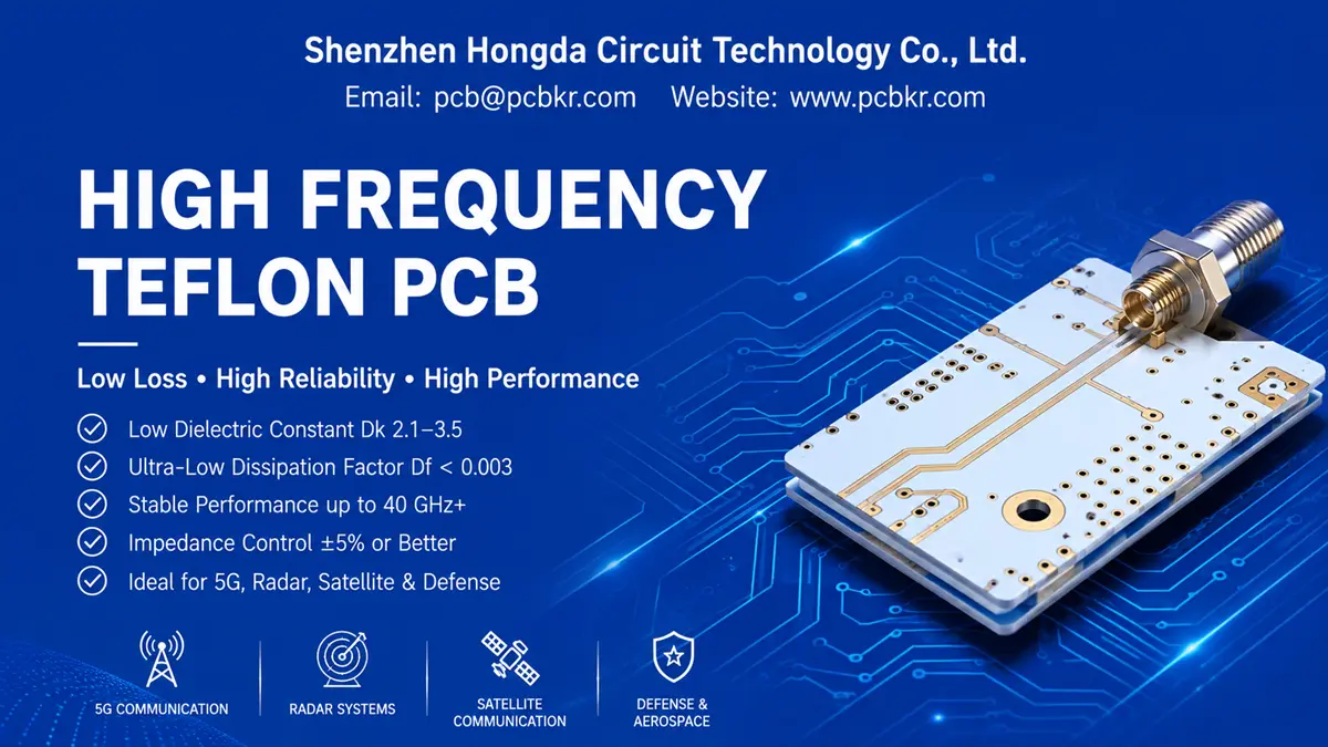
High Frequency Teflon PCB
When signal integrity determines system performance, engineers and procurement teams turn to High Frequency Teflon PCB solutions. Unlike standard FR-4 substrates that suffer from excessive dielectric loss above 1 GHz, PTFE-based laminates maintain stable electrical characteristics from microwave through millimeter-wave frequencies. Whether you are sourcing RF Teflon PCB assemblies for 5G-Advanced base stations, Microwave PCB substrates for phased array radar, or Low Loss PCB stacks for satellite downlink converters, material selection and manufacturing precision define the boundary between a functional prototype and a field-reliable product.
This guide is structured for B2B procurement professionals, hardware engineering managers, and RF system architects evaluating High Frequency Teflon PCB suppliers in 2026. We cover the technology trends, material science, manufacturing differentiators, and application-specific requirements that drive purchasing decisions in Telecom, Radar, Satellite, and Defense sectors.
What Is a High Frequency Teflon PCB?
A High Frequency Teflon PCB is a printed circuit board fabricated on polytetrafluoroethylene (PTFE) or PTFE-composite laminate, chosen specifically for its low dielectric constant (Dk ≈ 2.1–3.5) and ultra-low dissipation factor (Df < 0.003 at 10 GHz). These substrates minimize signal attenuation, phase distortion, and impedance variation across wide temperature and humidity ranges—properties that FR-4, with its Dk near 4.5 and Df above 0.02, cannot deliver at microwave frequencies.
PTFE Substrate Fundamentals and Composite Engineering
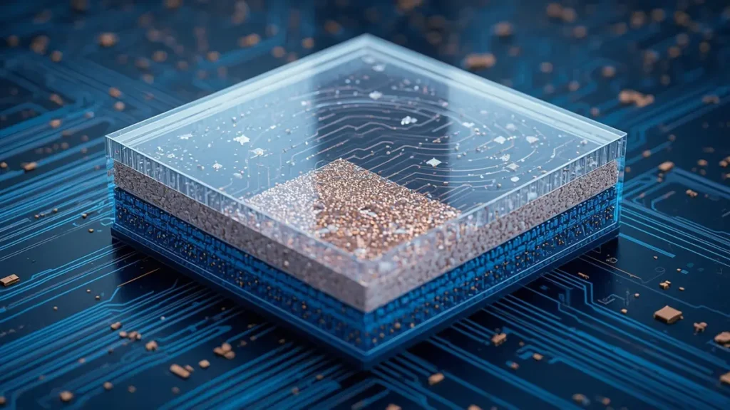
3D Cross-Section of PTFE Substrate with Ceramic Fillers – Hongda Circuit
Pure PTFE offers a Dk of approximately 2.0 and a loss tangent near 0.0003, but its high coefficient of thermal expansion (CTE) and mechanical softness require reinforcement for PCB fabrication. Leading material suppliers such as Rogers Corporation and Taconic integrate woven glass, ceramic fillers, or microfiber glass to improve dimensional stability without sacrificing electrical performance. The resulting composites—Rogers RO3003, RT5880, Taconic TLY-5, and TLX-8—provide the mechanical rigidity needed for multilayer lamination while preserving the low-loss characteristics that define Low Loss PCB performance.
For procurement teams, the critical specification is not simply “PTFE” but the specific composite grade, lot-controlled Dk tolerance (typically ±0.02), and copper foil roughness profile. At Shenzhen Hongda Circuit Technology Co., Ltd., we maintain qualified vendor lists (QVL) for Rogers, Taconic, and Isola materials, with full lot traceability from raw laminate through finished board—essential for AS9100D and defense contract compliance.
Why Teflon Outperforms Standard FR4 at Microwave Frequencies
Above 10 GHz, dielectric loss becomes the dominant channel impairment. FR-4’s epoxy resin absorbs electromagnetic energy, converting it to heat and raising the effective dissipation factor by 2–3× as frequency increases. PTFE’s fluoropolymer molecular structure, by contrast, exhibits minimal polarizability, yielding a Df that remains stable from 1 GHz to 40 GHz and beyond. This stability enables Microwave PCB designers to predict insertion loss accurately, maintain tight impedance control (±5% or better), and avoid the costly redesign cycles that plague FR-4-based RF prototypes.
RF Teflon PCB vs. Microwave PCB vs. Low Loss PCB
While these terms are often used interchangeably in supplier searches, each carries distinct procurement implications depending on frequency range, power handling, and environmental requirements.
RF Teflon PCB for Radio Frequency and Millimeter-Wave Applications
An RF Teflon PCB typically addresses frequencies from 300 MHz to 30 GHz, covering cellular infrastructure, microwave backhaul, and automotive radar at 77 GHz. Procurement specifications for RF Teflon PCB builds emphasize controlled impedance transmission lines, consistent dielectric thickness across the panel, and low-profile copper foil to minimize skin effect losses. At Hongda Circuit, our RF Teflon PCB process flow includes dedicated PTFE bake cycles, plasma desmear for through-hole metallization, and laser direct imaging (LDI) to eliminate phototool-induced pad-size variation—critical for impedance accuracy in microstrip and grounded coplanar waveguide (GCPW) structures.
Microwave PCB Design Considerations Above 10 GHz
A Microwave PCB pushes into the K-band (18–27 GHz), Ka-band (27–40 GHz), and beyond. At these frequencies, substrate thickness selection becomes a first-order design variable: thinner substrates (10–20 mil) reduce transverse resonance and suppress higher-order propagation modes. Microwave PCB procurement also demands hybrid stack-up expertise, combining PTFE RF layers with low-cost FR-4 or hydrocarbon ceramic digital layers to balance electrical performance with mechanical stability and total cost of ownership. Hongda’s engineering team provides stack-up optimization services that model insertion loss, thermal expansion mismatch, and lamination bonding compatibility before tooling commitment.
Low Loss PCB Material Selection: Dk, Df, and Copper Roughness
The term Low Loss PCB is the procurement umbrella under which material grades are compared quantitatively. Key parameters include:
- Dielectric Constant (Dk): Determines signal propagation velocity and transmission line geometry. Lower Dk (2.1–3.0) permits wider traces for a given impedance, easing manufacturability.
- Dissipation Factor (Df): Directly correlates with dielectric insertion loss. For 2026 designs, Df below 0.002 at 10 GHz is the baseline for 5G massive MIMO; W-band applications at 94 GHz demand Df below 0.0012.
- Copper Roughness (Rz): At microwave frequencies, current concentrates near the copper-dielectric interface. Lower Rz (< 2 μm) reduces conductor loss and improves return loss consistency.
Hongda Circuit qualifies every laminate lot with XRF spectrometry and automated thermal cycling to verify that Dk and Df remain within specification across the operating temperature range.
2026 Manufacturing Technology for High Frequency Teflon PCB
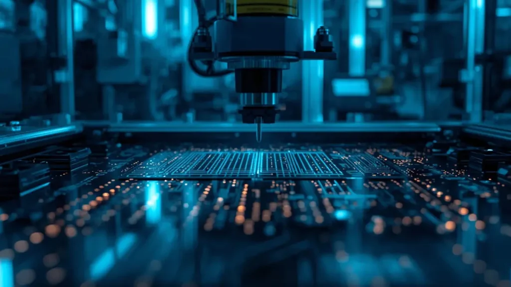
Laser Direct Imaging (LDI) Machine Processing RF Teflon PCB – Hongda Circuit
The gap between “capable of PTFE” and “qualified for production” widened significantly in 2026. AI infrastructure, 6G research, and defense modernization have pushed High Frequency Teflon PCB manufacturing toward semi-additive processes, sub-micron registration, and AI-enhanced inspection.
mSAP and Semi-Additive Processes for Fine-Line RF Structures
Traditional subtractive etching struggles to maintain trace uniformity below 50 μm line/space on soft PTFE substrates. The mSAP process PCB (modified semi-additive process) deposits a thin copper seed layer, patterns with LDI resist, and electroplates trace geometry before flash-etching the seed—enabling 8 μm/8 μm line/space with near-vertical sidewalls. For RF Teflon PCB designs featuring densely packed feed networks or interdigital filters, mSAP eliminates the trapezoidal trace profiles that cause impedance discontinuities. Hongda Circuit’s mSAP line ships production volumes for AI infrastructure and optical transceiver customers, with documented S-parameter reports and microsections available for procurement audit.
Hybrid Stack-Up Engineering: Combining PTFE with Digital Layers
Mixed-material Microwave PCB constructions require careful management of CTE mismatch, prepreg flow, and dielectric spacing during lamination. A typical hybrid combines Rogers RO4350B RF cores with standard FR-4 digital layers, bonded with compatible low-flow prepregs. Hongda’s LAUFFER lamination system applies z-axis pressure profiling and staged temperature ramps to prevent resin starvation, delamination, or dielectric thickness variation that would shift impedance targets. Our process engineers validate each hybrid stack-up with cross-sectional microscopy and time-domain reflectometry (TDR) before releasing to production.
Plasma Surface Activation and Controlled Lamination Cycles
PTFE’s low surface energy makes chemical metallization challenging. Sodium etch or plasma treatment is mandatory to create micro-roughness for electroless copper adhesion. Hongda Circuit operates inline plasma systems with process recipes tuned by laminate supplier and thickness, ensuring hole-wall pull strength exceeds IPC-6012 Class 3 requirements. For multilayer Low Loss PCB builds, we implement controlled lamination cycles with vacuum-assisted debulking to remove entrapped air—critical because voids at PTFE-glass interfaces become localized field concentrators that degrade breakdown voltage and long-term reliability.
Advanced Metrology: TDR, X-Ray, and 3D AOI for RF Validation
Procurement teams should demand more than basic electrical continuity. Hongda Circuit’s metrology suite includes:
- Nordson DAGE X-Ray Tester: 3D void detection in plated through-holes and microvias, performed before surface finish application.
- TDR Inline Screening: Automated impedance validation at ±5% tolerance for every high-speed differential pair.
- 3D AOI: Solder mask registration and trace geometry verification against design intent.
- XRF Spectrometers: Non-destructive gold/nickel thickness measurement with NIST-traceable calibration.
This equipment infrastructure, combined with IPC-6012 Class 3/3A process controls, provides the data package that aerospace and defense procurement officers require for first-article inspection.
High Frequency Teflon PCB Applications

High Frequency Teflon PCB Applications in 5G, Radar, and Satellite – Hongda Circuit
High Frequency Teflon PCB technology serves mission-critical systems where electrical performance stability and long-term reliability are non-negotiable. The following sectors represent the primary demand drivers in 2026.
Telecom Infrastructure and 5G-Advanced Massive MIMO
5G-Advanced base stations operating at 28 GHz and 39 GHz require phase-matched feed networks across 64T64R active antenna units. Each antenna array demands 0.5–2 square meters of Low Loss PCB substrate for radiating elements and RF transmission lines. PTFE-based laminates such as Rogers RO3003 and Taconic TLY-5 provide the Dk consistency and low Df necessary for beamforming accuracy. Hongda Circuit supplies High Frequency Teflon PCB panels for telecom OEMs with material certificates, impedance coupons, and full electrical test reports.
Radar Systems and Phased Array Antennas
Modern radar—whether civil weather monitoring or military fire control—relies on phased array architectures that steer beams electronically rather than mechanically. RF Teflon PCB substrates form the backbone of transmit/receive (T/R) modules, where phase stability across temperature cycles determines angular resolution. Rogers RT6000 and RT5000 series materials, with tightly controlled Dk values and long MIL-spec qualification histories, are standard for these applications. Hongda’s AS9100D-certified production lanes support defense and aerospace procurement with full material traceability and AS9102 first-article documentation.
Satellite Communications and Space-Grade Reliability
Satellite transponders, low-noise block downconverters (LNBs), and Ka-band user terminals operate in environments with extreme thermal cycling and radiation exposure. Microwave PCB substrates for space applications must exhibit low outgassing, stable Dk across −55°C to +125°C, and resistance to ionizing radiation. PTFE’s inherent chemical inertness and low moisture absorption (< 0.1%) make it the substrate of choice for geostationary and low-earth-orbit hardware. Hongda Circuit provides satellite-qualified Low Loss PCB builds with thermal cycling validation and scanning acoustic microscopy (SAM) for void-free dielectric layers.
Defense Electronics and Electronic Warfare
Electronic warfare (EW) systems, software-defined radios, and signals intelligence platforms demand the lowest possible dielectric loss at frequencies above 40 GHz. High Frequency Teflon PCB materials such as Rogers RT/duroid 5870 (Dk 2.33, Df 0.0012) enable compact, high-performance RF front-ends where every decibel of insertion loss directly impacts system sensitivity. Defense procurement requires not only performance but also supply chain security; Hongda Circuit’s vertically integrated fabrication—no third-party subcontracting for core processes—ensures IP protection and lot traceability from raw material to finished goods.
Why Procurement Teams Choose Shenzhen Hongda Circuit Technology
Selecting a High Frequency Teflon PCB supplier is a technical due-diligence exercise. Procurement managers, hardware directors, and quality engineers evaluate capability, documentation, and risk mitigation. Here is how Hongda Circuit (PCBKR) addresses each checkpoint in the 2026 procurement decision chain.
Vertically Integrated PTFE PCB Fabrication from Prototype to Volume
Hongda Circuit operates complete in-house production lines for PTFE-based RF Teflon PCB, Microwave PCB, and Low Loss PCB constructions. From material incoming inspection through final electrical test and serialization, no critical process is outsourced. This vertical integration eliminates the communication gaps, quality variance, and IP exposure risks common in multi-vendor supply chains. We support prototype quantities (5–10 pieces, 10–15 business days) through high-volume production (1,000+ pieces, 3–7 weeks) with consistent process parameters.
2026 Equipment Suite: LDI, Laser Drilling, and Automated Plating
Our Baoan, Shenzhen facility has completed a full equipment upgrade aligned with 2026 high-frequency manufacturing requirements:
- SCREEN Ledia LDI Exposure Machine: Direct imaging for soldermask and etch resist, eliminating phototool degradation that causes pad-size variation and plating non-uniformity.
- Mitsubishi UV/CO₂ Hybrid Laser Drilling: Microvia formation down to 0.075 mm (75 μm) with zero residual stub for blind via designs.
- LAUFFER Lamination System: Z-axis pressure profiling for hybrid PTFE/FR-4 stack-ups, preventing resin smear and dielectric thickness drift.
- HX Automated Plating Line: Consistent copper deposition for through-hole reliability and mSAP trace geometry.
- Nordson DAGE X-Ray and 3D AOI: 100% structural validation before surface finish.
This equipment list is not marketing copy—it is the actual production floor configuration that supports our 224G PAM4 backplane and PTFE RF qualifications.
Certifications That Matter: AS9100D, IATF 16949, and IPC-6012 Class 3
Certification alignment is a non-negotiable filter in B2B supplier selection. Hongda Circuit maintains:
- ISO 9001:2015/2026 (Quality Management)
- AS9100D (Aerospace & Defense)
- IATF 16949:2016 (Automotive)
- ISO 13485:2016 (Medical Devices)
- IPC-6012 Class 3/3A (High-Reliability Performance)
- UL Recognition for flame resistance and safety
For defense and aerospace procurement, these certifications provide independent verification that our quality management system meets the same standards expected of Western suppliers—at competitive total cost of ownership.
Engineering-First DFM Reviews and 24-Hour Quotation Response
The most expensive RF PCB is the one that fails in qualification due to a manufacturability oversight. Hongda Circuit’s DFM team reviews every incoming design for impedance continuity, via antipad optimization, thermal management, and lamination compatibility—before tooling begins. This collaborative workflow reduces design iterations, cuts prototyping costs, and accelerates time-to-market. Procurement teams receive a detailed quotation, DFM analysis, and recommended stack-up within 24 hours of Gerber submission.
Contact:sales@pcbkr.com | Phone: +86 0755 23720053 | Website:www.pcbkr.com
High Frequency Teflon PCB for Telecom, Radar, Satellite, and Defense
In 2026, High Frequency Teflon PCB technology is no longer a niche specialty—it is a foundational enabler for 5G-Advanced infrastructure, next-generation radar, satellite constellations, and defense modernization programs. Whether your specification calls for RF Teflon PCB with mSAP fine-line processing, Microwave PCB hybrid stack-ups for Ka-band terminals, or Low Loss PCB substrates with AS9100D traceability, the manufacturing partner you choose determines whether your design intent survives the transition from simulation to field deployment.
Shenzhen Hongda Circuit Technology Co., Ltd. (PCBKR) combines 2026-leading High Frequency Teflon PCB manufacturing technology with the agility, engineering responsiveness, and transparent quality systems that tier-1 procurement teams demand. From DFM review to final delivery, we operate as your technical partner—not merely your vendor.
Ready to validate your next RF design? Submit your Gerber files and stack-up requirements to sales@pcbkr.com for a complimentary DFM review, impedance simulation, and competitive quotation within 24 hours.
Frequently Asked Questions: High Frequency Teflon PCB Procurement
How do I verify that a Teflon PCB manufacturer can actually build high-frequency boards, not just quote them?
Request documented evidence of PTFE-specific process controls: plasma or sodium etch protocols for metallization, dedicated PTFE lamination cycles, and impedance validation data (TDR or VNA S-parameters) from previous builds. Verify that their equipment list includes LDI exposure (not conventional phototools), laser drilling for microvias, and X-ray inspection for void detection. At Hongda Circuit, we provide microsections, S-parameter reports, and first-article inspection packages for every High Frequency Teflon PCB order.
What is the difference between Rogers RO3003 and Taconic TLY-5 for microwave applications?
Both are ceramic-filled PTFE composites optimized for low loss, but they differ in Dk, Df, and thermal properties. RO3003 offers Dk 3.0 and Df 0.0013 at 10 GHz with excellent Dk stability across temperature, making it ideal for 77 GHz automotive radar and 5G mmWave. TLY-5 provides Dk 2.2 and Df 0.0009, preferred for satellite and defense applications where the lowest possible insertion loss is critical. Your fabricator should maintain qualified stocks of both and recommend based on your frequency, thermal, and cost targets.
Why does my RF Teflon PCB quote vary so much between suppliers for the same Gerber files?
Price variance stems from material grade (commercial vs. MIL-spec lot control), copper foil type (standard ED vs. low-profile RT), surface finish (ENIG vs. ENEPIG for wire bonding), and inspection depth (basic e-test vs. 100% TDR + X-ray). Some suppliers quote standard FR-4 processes adapted to PTFE, while others use dedicated RF manufacturing lanes with controlled humidity, plasma treatment, and specialized drill parameters. Always request a process flow comparison, not just a price comparison.
What certifications should I demand from a Teflon PCB supplier serving aerospace or defense programs?
Minimum requirements are ISO 9001, IPC-6012 Class 3, and AS9100D for aerospace. For defense electronics, verify ITAR registration (if US-controlled) or equivalent export compliance, and demand full material lot traceability per AS9102. IATF 16949 indicates automotive-grade process discipline, which correlates with consistent RF performance. Hongda Circuit maintains ISO 9001, AS9100D, IATF 16949, ISO 13485, and IPC-6012 Class 3/3A certifications with full documentation packages.
How does hybrid stack-up design affect manufacturability and cost in Microwave PCB builds?
Hybrid Microwave PCB constructions combine PTFE RF layers with FR-4 or hydrocarbon ceramic digital layers to optimize cost and performance. However, CTE mismatch between materials can cause delamination or via barrel cracking during thermal cycling. Successful hybrids require compatible prepreg selection, staged lamination pressure profiles, and careful drill parameter optimization for each material layer. A qualified manufacturer will model these interactions during DFM and recommend stack-up adjustments before committing to tooling—saving weeks of redesign and qualification time.
Company: Shenzhen Hongda Circuit Technology Co., Ltd. (PCBKR)
Address: Room 1608-1610, R&D Comprehensive Building, Baoyunda Logistics Center, Bao’an District, Shenzhen, China
Organization Code: 91440300MA5F6CA091
Website: www.pcbkr.com
Email: sales@pcbkr.com
Phone: +86 0755 23720053
Certifications: ISO 9001:2015 | AS9100D | IPC-6012 Class 3/3A | ISO 13485 | IATF 16949 | UL
About Author
David Chen https://www.linkedin.com/in/pcbcoming
David Chen boasts an extensive professional background in PCBA manufacturing, PCBA testing, and PCBA optimization, with specialized expertise in high-precision PCBA fault analysis and rigorous PCBA reliability testing. The author has worked with high-layer-count server PCB fabrication, ultra-low-loss backplane stackups, and thermo-mechanical reliability optimization for AI infrastructure projects involving 112G and 224G PAM4 architectures. Skilled in complex circuit design and cutting-edge advanced PCB manufacturing processes, he delivers solutions that elevate product durability and performance across industrial applications. His technical articles focusing on PCBA manufacturing workflows and testing methodologies are widely cited by industry peers, research institutions, and technical platforms, solidifying his reputation as a recognized technical authority in the global circuit board manufacturing sector.