Ultra-Thin LCD PCB Procurement Guide 2026: How to Source High-Density Flexible Circuits for Display Modules Without Supply Chain Risk
Ultra thin LCD PCB serves as a core foundational component for lightweight, high-precision display modules, and its market development is closely tied to the booming demand for smart terminal and automotive display products. Driven by the widespread demand for thinner, lighter and more sophisticated flexible circuits in smartphones, automotive displays and wearable display modules, the global High-Density Interconnect (HDI) PCB market is projected to hit a market value of $19.47 billion by 2026.
This robust market growth brings a dual-edged impact on procurement managers overseeing LCD display supply chains, presenting both valuable market opportunities and prominent operational risks. On the opportunity side, the expanding market scale has attracted a growing number of suppliers to layout ultra-thin Flexible Printed Circuit (FPC) manufacturing businesses, enriching the overall supplier pool for ultra thin LCD PCB sourcing. However, the industry currently faces a severe capability differentiation problem: while numerous suppliers claim to have ultra-thin FPC manufacturing qualifications, only a handful of them are equipped with the core capabilities required for stable and high-volume production, including professional laser drilling precision, perfect ACF bonding compatibility, and standardized IPC Class 3 quality management systems.
Against this industry backdrop, this guide focuses on the full-process procurement decision logic for ultra thin LCD PCB sourcing. Different from general specification-based procurement documents, it conducts in-depth analysis of core manufacturing technologies, standardized testing protocols and scientific supplier evaluation criteria throughout the sourcing chain. Its core purpose is to help display module project teams avoid two key industry pain points — delayed project delivery caused by insufficient supplier capacity and costly on-site product failures that occur months after product launch, thereby ensuring the stable, reliable and sustainable operation of LCD display module programs.
What Is an Ultra-Thin LCD PCB and Why Procurement Teams Are Reassessing Suppliers in 2026
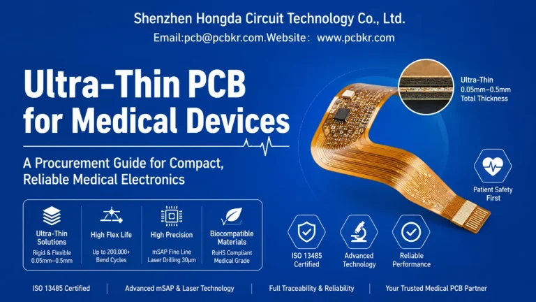
An ultra-thin LCD PCB—also referred to as an ultra-thin FPC for display modules—is a flexible printed circuit specifically engineered to interconnect LCD panels with driver ICs, backlight systems, and touch controllers. These circuits typically operate within a thickness range of 0.05 mm to 0.40 mm (50 μm to 400 μm), enabling OEMs to achieve the slim profiles now standard in smartphones, tablets, automotive clusters, and medical portables.
Unlike standard flexible PCBs used in simple cable replacements, LCD driver FPCs must manage high-density signal routing, controlled impedance for MIPI/LVDS lines, and mechanical reliability through repeated flex cycles. The transition to high-resolution panels (WQHD+, 4K mobile displays) has pushed typical layer counts to 4-layer (1+2+1) or 6-layer (2+2+2) stack-ups, with line widths and spaces shrinking to 2 mil (50 μm) or below.
Several market forces are compelling procurement teams to requalify their flexible PCB supplier base in 2026:
- Integrated touch adoption: TDDI (Touch Display Driver Integration) and in-cell touch technologies eliminate separate touch assemblies, reducing module thickness but increasing FPC complexity.
- Automotive display growth: EV and ADAS ecosystems are expanding demand for HDI PCBs in infotainment and instrument cluster displays.
- Copper and laminate volatility: Raw material price surges have exposed the risk of sourcing from suppliers without vertical integration or inventory depth.
For buyers, the implication is clear: the lowest unit price quote often masks hidden costs in rework, delayed deliveries, and latent reliability defects that only surface during module assembly or end-customer use.
Critical Specifications Every LCD Display Buyer Must Verify Before Sourcing Ultra-Thin FPC
Procurement teams frequently receive quotes based on Gerber files without understanding whether the supplier’s process can reliably manufacture to the tolerances required for LCD modules. Before issuing a purchase order, verify these five specification categories:
Layer Stack-Up and Microvia Density for High-Density Interconnect LCD Driver Boards
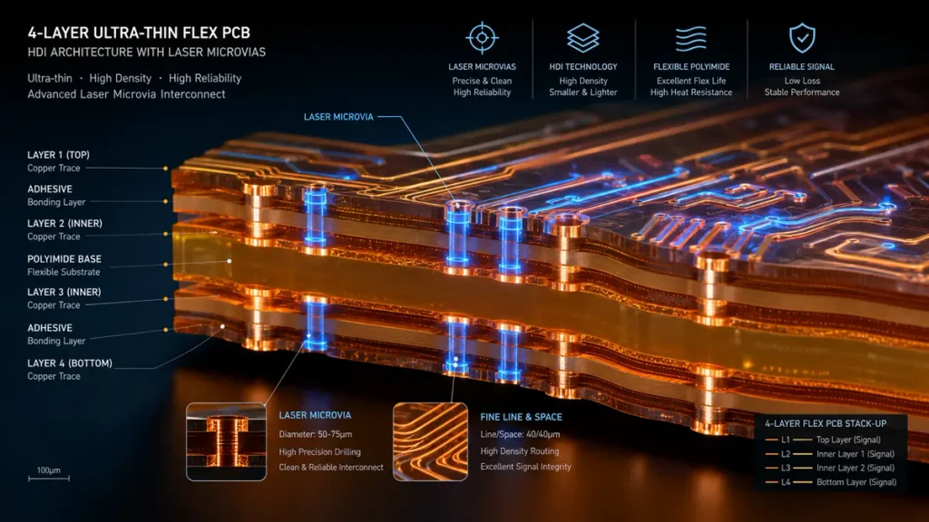
4-Layer Ultra-Thin Flex PCB Layer Stack-Up & Laser Microvia Architecture
Modern ultra-thin LCD PCBs for driver applications rarely use single-sided construction. A 4-layer FPC (L4) with blind microvias connecting L1-L2 and L3-L4 is now the baseline for mid-resolution panels. High-end smartphone displays often require 6-layer or 8-layer flexible circuits with stacked or staggered microvias.
The critical parameter here is microvia aspect ratio—the ratio of via depth to finished diameter. IPC-2226 and IPC-6018 define a maximum aspect ratio of 1:1 for reliable microvia fabrication, with preferred ratios between 0.75:1 and 0.8:1 to ensure uniform copper plating and minimize voids. Exceeding 1:1 increases plating void rates by over 40% and creates corner crack initiation points during thermal cycling.
For a typical 4-layer ultra-thin FPC with 60 μm dielectric thickness between L1-L2, this means the microvia diameter should not be smaller than 75 μm (3 mil), and ideally 80–100 μm for production robustness.
Trace and Space Tolerances for Fine-Pitch Display Interconnects
High-resolution LCD panels route hundreds of signals through extremely narrow edge areas. The Line/Space (L/S) capability of your FPC supplier directly determines whether your design is manufacturable. For 2026 display modules:
- Standard capability: 3 mil / 3 mil (75 μm / 75 μm)
- Advanced capability: 2 mil / 2 mil (50 μm / 50 μm) or finer
- Cutting-edge (LDI-based): 25 μm / 25 μm using Laser Direct Imaging
If your LCD driver IC uses a 0.3 mm pitch BGA or COG (Chip-on-Glass) bonding, the escape routing on the FPC demands these fine tolerances. Suppliers still relying on traditional photolithography with contact printers cannot consistently hold 2 mil L/S over production volumes. Laser Direct Imaging (LDI) has become the differentiating technology for ultra-fine circuit fabrication.
Surface Finish and ACF Bonding Compatibility
For LCD module assembly, the FPC terminates in gold fingers that bond to the glass panel’s ITO pads or to the driver IC via Anisotropic Conductive Film (ACF). This thermocompression process—typically operating at 180–210°C with 2–4 MPa pressure for 10–20 seconds—demands a surface finish that provides both oxidation resistance and consistent contact resistance.
Electroless Nickel Immersion Gold (ENIG) is the dominant surface finish for display FPCs. The nickel layer (typically 3–6 μm) provides a diffusion barrier, while the immersion gold (0.05–0.10 μm) ensures solderability and ACF compatibility. For ultra-fine pitch applications, ENEPIG (Electroless Nickel Electroless Palladium Immersion Gold) is increasingly specified to eliminate the “black pad” risk associated with high-phosphorus ENIG on nickel.
Procurement tip: Verify that your supplier’s ENIG process is optimized for ACF bonding, not just SMT soldering. ACF-compatible ENIG requires a flatter surface profile (Ra < 0.3 μm) to ensure uniform particle deformation across all pads during thermocompression.
Material Selection: Modified PI vs. FR-4 Composite Substrates
The substrate material determines both the mechanical flexibility and the signal integrity of your ultra-thin LCD PCB. Two material systems dominate in 2026:
- Polyimide (PI) Film: Standard for dynamic flex applications. Modified PI formulations with low-Dk (dielectric constant ≈ 3.2–3.4) and low-Df (dissipation factor < 0.003) are now available for high-speed MIPI DSI signaling. PI thicknesses range from 12.5 μm (1/2 mil) to 25 μm (1 mil) for ultra-thin constructions.
- FR-4/PI Composites: Used in rigid-flex or stiffened areas where component mounting or connector insertion requires mechanical stability. High-Tg FR-4 cores (Tg > 170°C) prevent delamination during lead-free reflow and ACF bonding thermal exposure.
For automotive display modules operating across -40°C to +105°C temperature ranges, material selection must account for CTE (Coefficient of Thermal Expansion) mismatch between copper traces and the substrate. Suppliers with in-house material characterization capabilities can simulate this mismatch during DFM review—a significant advantage over brokers who simply forward files to anonymous factories.
Stiffener Strategy and Dynamic Flex Reliability
Not every region of an LCD driver FPC needs to flex. Stiffeners—typically FR-4, PI, or stainless steel—are laminated to areas carrying connectors, components, or undergoing assembly stress. However, excessive stiffener coverage increases weight, thickness, and cost.
A competent supplier will recommend selective stiffener placement based on your assembly process:
- Connector areas: FR-4 stiffener (0.2–0.5 mm) to prevent pad lifting during insertion
- Component mounting zones: PI or epoxy stiffener for SMT compatibility
- Dynamic flex regions: No stiffener; use rolled annealed (RA) copper rather than electrodeposited (ED) copper to improve flex life from ~50,000 cycles to over 1,000,000 cycles
The bend radius is equally critical. IPC-2223 recommends a minimum bend radius of 3× the total circuit thickness for static applications and 5× to 10× for dynamic flexing. For a 0.15 mm thick 4-layer FPC, this translates to 0.75 mm minimum dynamic bend radius. Suppliers without experience in bend radius optimization often approve designs that fail within 6 months in foldable or hinge-mounted displays.
Advanced Manufacturing Technologies That Separate Tier-1 Ultra-Thin PCB Manufacturers from Trading Companies
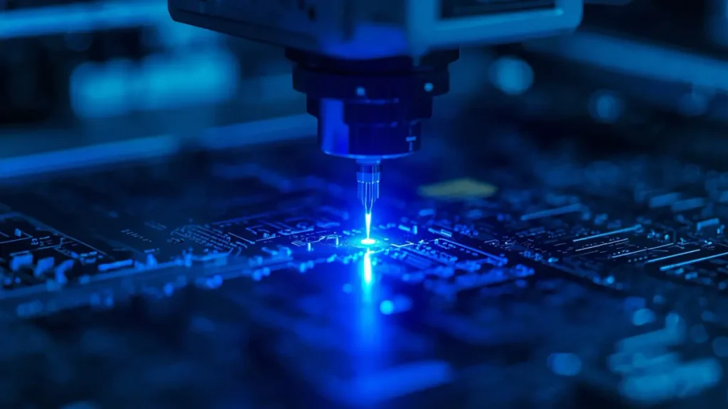
Hybrid UV Laser Drilling Process for Ultra-Thin Flexible PCB
The gap between a catalog claim and actual production capability is where most ultra-thin FPC procurement failures originate. When auditing a potential supplier—or evaluating your incumbent—inspect for these five technology differentiators:
Hybrid CO₂/UV Laser Drilling for Microvia Formation
Mechanical drilling cannot reliably produce holes below 150 μm in diameter. For HDI microvias in display driver FPCs, laser drilling is non-negotiable. However, not all laser systems deliver equivalent results:
- CO₂ lasers (10.6 μm wavelength): Fast ablation of dielectric materials (PI, FR-4 prepreg) but reflect off copper. Requires pre-patterned copper windows, limiting minimum via size to ~75 μm.
- UV lasers (355 nm wavelength): Ablate both copper and dielectric, enabling direct drilling without windowing. Capable of 25–50 μm vias with minimal heat-affected zone (< 10 μm).
- Hybrid systems: Integrate UV opening with CO₂ dielectric removal, optimizing both precision and throughput.
A Tier-1 ultra-thin LCD PCB manufacturer operates hybrid laser drilling with CCD vision alignment (±5 μm accuracy) and real-time energy compensation to account for material thickness variation. They also perform spiral scanning for ultra-fine vias rather than simple single-point drilling, producing smoother hole walls that improve plating adhesion and reduce voids.
At Shenzhen Hongda Circuit Technology, our microvia capability extends to 50 μm diameter on 40 μm dielectric (0.8:1 aspect ratio), with 100% cross-section verification per IPC-6018 on all HDI orders.
Laser Direct Imaging (LDI) for Sub-50μm Trace Precision
Traditional contact printing uses photomasks that introduce edge roughness and alignment errors. For 2 mil (50 μm) traces and below, LDI exposes photoresist directly using UV lasers, eliminating mask distortion and achieving ±2 μm registration accuracy.
LDI is particularly critical for COG (Chip-on-Glass) and FOG (Film-on-Glass) bonding areas, where the FPC gold finger pitch must match the glass panel ITO pad pitch within ±10 μm. A supplier without LDI capability may quote these tolerances but struggle to maintain them across production lots, leading to misalignment failures during ACF thermocompression.
Roll-to-Roll Processing for High-Volume FPC Production
For display module programs exceeding 100,000 units per month, roll-to-roll (R2R) manufacturing provides significant cost and consistency advantages over sheet-based processing. R2R lines continuously process PI-copper laminate from reel to reel, enabling:
- Etch uniformity: Better chemistry control and consistent dwell times
- Automated optical inspection: Inline AOI at each process stage
- Material traceability: Lot-controlled substrate tracking from incoming inspection to shipment
Suppliers relying solely on sheet processing for high-volume orders often encounter lot-to-lot variation in trace width and dielectric thickness—variation that manifests as impedance mismatch and signal integrity issues in your LCD module.
AOI, Flying Probe, and X-Ray Inspection Protocols
Testing is not a single event; it is a series of gates. For ultra-thin LCD PCBs, a robust test strategy combines:
- Automated Optical Inspection (AOI): 100% coverage after etching and after surface finish. Detects trace width deviations, open circuits, and solder mask defects. Modern 3D AOI systems measure trace height and surface topology, catching issues invisible to 2D cameras.
- Flying Probe Testing (FPT): Electrical verification without custom fixtures. Ideal for prototypes and low-to-medium volume (5–500 boards). Flying probes verify continuity, isolation, and component values with 5–15 μm positioning accuracy. For ultra-thin FPCs, FPT is preferred over ICT because it eliminates mechanical stress from bed-of-nails fixtures that can crack microvias or delaminate thin substrates.
- X-Ray Inspection (AXI): Required for stacked microvias and buried via structures. X-ray verifies copper fill density and detects voids that electrical testing cannot identify. For Class 3 medical or aerospace display modules, X-ray inspection of microvia fill is mandatory per IPC-6018.
- Impedance Testing (TDR): For high-speed LCD driver boards carrying MIPI or eDP signals, Time Domain Reflectometry verifies that differential pairs maintain ±5% of target impedance (typically 100 Ω ± 5 Ω).
Suppliers who quote “100% electrical testing” but only perform manual visual inspection are creating liability for your program. Demand documentation of the specific test methods applied to your lot.
COG/FOG ACF Bonding Process Control and Yield Optimization
The final assembly step—bonding your ultra-thin FPC to the LCD glass—depends critically on FPC pad flatness, cleanliness, and dimensional stability. A supplier with in-house COG/FOG bonding capability or deep process integration with LCM (Liquid Crystal Module) assemblers can provide:
- Pre-bonding plasma cleaning to remove organic contamination from ENIG pads
- Particle control: Class 100–1000 cleanroom compatibility for FPC packaging
- Bonding parameter optimization: Temperature profiles (180–210°C), pressure (2–4 MPa), and dwell time (10–20 s) validated against your specific ACF material and glass substrate
- Post-bonding pull testing: Mechanical validation of bond strength per ASTM F1269
Suppliers without ACF bonding expertise often deliver FPCs with surface contamination or excessive nickel roughness that causes ACF particle embedding inconsistency—resulting in intermittent open circuits after module assembly.
Shenzhen Hongda Circuit Technology Co., Ltd. — Capabilities and Certifications for Display Module FPC
Established in 1999 and headquartered in Shenzhen, Shenzhen Hongda Circuit Technology Co., Ltd. (www.pcbkr.com) has evolved from a standard PCB fabricator to a specialist in high-density interconnect flexible circuits for display, RF, and automotive applications. Our facility occupies over 100,000 square meters with 10+ production lines and 100+ R&D engineers.
Manufacturing Technology Portfolio
Our 2026 advanced manufacturing infrastructure specifically supports ultra-thin LCD PCB programs:
- Hybrid Laser Drilling: CO₂ + UV laser systems capable of 50 μm microvias with aspect ratios ≤0.8:1, supported by high-resolution CCD alignment and spiral scanning for optimal hole wall quality
- LDI Fine-Line Fabrication: 25 μm line/space capability for high-density driver IC escape routing
- Roll-to-Roll Processing: Continuous production lines for high-volume FPC orders, reducing unit cost and improving lot consistency
- Sequential Lamination: 4-layer to 16-layer flexible and rigid-flex stack-ups with buried and blind microvia structures
- Advanced Surface Finishes: ENIG (2–5 μm Ni / 0.05–0.1 μm Au), ENEPIG, and OSP, optimized for ACF bonding compatibility
Quality System and Certifications
- ISO 9001: Quality management system baseline
- IATF 16949: Automotive quality standards for display modules used in EV and ADAS applications
- ISO 13485: Medical device quality management for diagnostic and patient-monitoring displays
- UL Certification: Flame retardancy (UL94 V-0) and electrical safety recognition
- RoHS/REACH: Full material compliance for EU and North American markets
- IPC-6012 Class 2/3: Rigid PCB performance standards; IPC-6018 for HDI structures
DFM and Technical Support
We provide 24-hour DFM review upon Gerber submission, with specific focus on:
- Microvia aspect ratio validation against IPC-2226
- Bend radius analysis for dynamic flex regions
- Impedance stack-up optimization for high-speed display interfaces
- Stiffener placement recommendations based on assembly process
- ACF bonding pad design rules for COG/FOG compatibility
Our typical lead times are 3–5 days for ultra-thin FPC prototypes and 7–10 days for small-batch production, with full traceability documentation including material certificates, process parameters, and electrical test reports.
How to Evaluate an Ultra-Thin LCD PCB Supplier: A Procurement Decision Framework
Selecting a supplier based on unit price alone is the most common sourcing mistake in flexible PCB procurement. The following five-step framework protects your program from hidden costs and supply chain disruption.
Step 1 — Verify Fabrication Technology, Not Just Catalog Claims
Request documentation of:
- Laser drilling equipment: CO₂, UV, or hybrid? What is the minimum microvia diameter and aspect ratio capability?
- Imaging technology: LDI or contact printer? What is the finest L/S achieved in production (not just in R&D)?
- Lamination capability: Maximum layer count for flexible builds? Can they handle modified PI or LCP (Liquid Crystal Polymer) substrates?
- Plating chemistry: Do they use pulse reverse plating for high-throw microvia filling, or standard DC plating?
If a supplier cannot provide equipment model numbers, process capability studies (Cp/Cpk), or cross-section photos of actual production microvias, treat their claims as unverified.
Step 2 — Demand DFM Review Before Quoting
A supplier who quotes from your Gerber without engineering review is merely taking an order, not partnering on manufacturability. A legitimate ultra-thin LCD PCB manufacturer will flag:
- Trace width violations near microvia pads
- Insufficient annular rings for laser drill registration tolerance
- Impedance discontinuities at layer transitions
- Bend radius violations in dynamic flex regions
- ACF pad design issues (insufficient pitch, wrong surface finish)
At Shenzhen Hongda Circuit Technology, our engineering team performs DFM analysis within 24 hours and provides a formal report with recommended modifications before production commitment.
Step 3 — Validate Testing Protocols and IPC Class Compliance
Ask for the supplier’s standard test plan for your product category. For display module FPCs, the minimum acceptable test stack should include:
| Test Method | Purpose | Coverage |
|---|---|---|
| AOI (3D) | Visual defect detection | 100% post-etch, post-finish |
| Flying Probe | Electrical continuity/isolation | 100% for prototypes; sampling for volume |
| Microsection | Via wall quality, plating thickness | 5 coupons per panel, per IPC-6018 |
| TDR Impedance | Controlled impedance verification | 100% for high-speed designs |
| X-Ray (AXI) | Stacked microvia fill verification | 100% for Class 3; sampling for Class 2 |
| Thermal Stress | Solder float or IST cycling | Per IPC-TM-650 2.6.27 |
Suppliers who resist providing test data or claim “we test to IPC standards” without specifying the exact methods and sample sizes are cutting corners that will eventually fail in your application.
Step 4 — Assess Supply Chain Resilience and Material Traceability
In 2026, geopolitical tensions and raw material volatility have made supply chain resilience a procurement priority. Evaluate your supplier on:
- Substrate inventory: Do they stock PI films, copper foils, and coverlays from multiple qualified vendors, or rely on single-source just-in-time delivery?
- Material traceability: Can they provide lot-specific material certificates (UL, RoHS, TDS) with full forward/backward traceability?
- Vertical integration: Do they perform critical processes in-house (laser drilling, LDI, plating, AOI), or subcontract to uncertified third parties?
- Business continuity: What is their backup plan for equipment failure or power disruption?
Shenzhen Hongda Circuit Technology maintains strategic inventory of modified PI, high-Tg FR-4, and Rogers high-frequency laminates, with full MES-based traceability from incoming material to finished goods.
Step 5 — Calculate Total Cost of Ownership, Not Unit Price
The true cost of an ultra-thin LCD PCB includes:
- Unit price: The quoted per-piece or per-panel cost
- DFM rework: Engineering hours spent fixing design issues the supplier should have caught
- Yield loss: Boards scrapped due to manufacturing defects (who pays for scrap?)
- Field failure cost: Warranty claims, recalls, and brand damage from latent defects
- Inventory cost: Long lead times forcing you to hold safety stock
- Logistics cost: Shipping, customs, and duties
A supplier quoting $0.50 per piece but delivering 85% yield with 8-week lead times is more expensive than a supplier at $0.80 with 98% yield and 2-week delivery. Run this calculation explicitly for each vendor under consideration.
Application-Specific Sourcing: Matching FPC Technology to Your Display Module Requirements
Different display applications impose distinct mechanical, thermal, and electrical requirements on the flexible PCB. Match your sourcing strategy accordingly:
Smartphone and Tablet LCD Driver Boards
- Thickness target: 0.08–0.15 mm total
- Layer count: 4–6 layers with blind microvias
- Critical spec: 2 mil L/S, impedance control for MIPI DSI (100 Ω differential)
- Surface finish: ENIG optimized for ACF bonding
- Supplier priority: LDI capability, quick-turn prototype support (3–5 days), experience with high-volume R2R production
Automotive Dashboard and Infotainment Displays
- Thickness target: 0.15–0.25 mm (stiffer due to component load)
- Layer count: 4–8 layers with buried vias for noise isolation
- Critical spec: IATF 16949 certification, thermal cycling (-40°C to +105°C), high-voltage isolation (CAF resistance)
- Surface finish: ENEPIG or ENIG with extended nickel thickness for corrosion resistance
- Supplier priority: Automotive quality system, material characterization for CTE matching, PPAP documentation capability
Industrial HMI and Medical Display Equipment
- Thickness target: 0.20–0.40 mm (ruggedized)
- Layer count: 2–4 layers; reliability over density
- Critical spec: IPC-6012 Class 3, extended temperature range, long product lifecycle support (5–10 years)
- Surface finish: ENIG or immersion silver
- Supplier priority: ISO 13485 (medical), long-term material allocation agreements, comprehensive test documentation
Aerospace and Avionics Display Systems
- Thickness target: 0.10–0.20 mm (weight-critical)
- Layer count: 4–6 layers with staggered microvias (no stacking due to thermal stress)
- Critical spec: AS9100D, outgassing compliance (ASTM E595), extreme thermal shock (-55°C to +125°C)
- Surface finish: ENEPIG or gold over nickel
- Supplier priority: ITAR registration (if US defense), full material and process traceability, qualification test reporting per IPC-6018
Frequently Asked Questions by Procurement Managers Sourcing Ultra-Thin LCD PCBs
What is the minimum realistic lead time for ultra-thin LCD FPC prototypes, and what factors extend it?
For a 4-layer ultra-thin FPC with microvias and ENIG finish, capable suppliers deliver prototypes in 3–5 days if the design passes DFM without major revisions. Factors that extend lead time include: complex rigid-flex constructions (add 2–3 days), non-standard materials requiring procurement (add 3–7 days), and designs requiring iterative DFM corrections (add 1–2 days per revision). Suppliers quoting 2+ weeks for simple 4-layer FPC prototypes likely lack in-house laser drilling or are subcontracting the work.
How do I verify that a supplier’s ENIG surface finish is truly compatible with ACF bonding, not just standard SMT soldering?
Request three pieces of evidence: (1) surface roughness data (Ra < 0.3 μm measured by profilometer), (2) nickel phosphorus content (7–9% P for optimal ACF particle embedding, avoiding high-phosphorus formulations that reduce ductility), and (3) ACF bonding validation report showing pull test results (typically > 6 N/mm for 1 mm pitch) and cross-sections of particle deformation (60% compression ratio). Suppliers who only provide solderability test data (wet balance, spread test) have not validated their ENIG for display module assembly.
What is the difference between staggered and stacked microvias, and which should I specify for my LCD driver FPC?
Stacked microvias align vertically (L1-L2 directly above L2-L3), maximizing routing density but creating a copper-copper interface that is mechanically weaker under thermal cycling. Staggered microvias offset horizontally between layers, distributing stress and improving reliability by 20–30% in thermal shock testing. For smartphone LCD driver boards where space is absolute priority, 2-level stacked microvias are acceptable with copper fill and X-ray validation. For automotive, medical, or aerospace displays, staggered microvias are mandatory per IPC-6012 Class 3 guidelines. Always specify your requirement explicitly; suppliers may default to stacked vias to reduce lamination cycles unless instructed otherwise.
Why does my ultra-thin FPC supplier’s quoted price vary by 40% for the same Gerber file, and how do I identify the hidden cost drivers?
Price variance stems from four sources: (1) Material grade: One supplier quotes standard PI while another uses low-Dk modified PI without clarifying the difference. (2) Testing depth: The lower quote may omit microsection analysis, impedance testing, or thermal stress validation. (3) Yield assumption: The cheapest quote often assumes 85% yield and passes scrap costs to you via NCNR (non-cancelable, non-returnable) terms. (4) Process capability: A supplier with older contact printers may quote lower because they cannot reliably manufacture 2 mil traces and plan to request design relaxation after order acceptance. To identify hidden costs, require each supplier to submit a detailed Process Flow and Test Plan with their quote, then compare line-by-line.
What certifications are genuinely essential for an automotive display FPC supplier, and which are merely marketing badges?
For automotive display modules, IATF 16949 is non-negotiable—it mandates defect prevention, continuous improvement, and customer-specific requirements that generic ISO 9001 suppliers ignore. UL recognition (UL94 V-0 for flammability, UL796 for electrical safety) is required for North American market access. IPC-6012 Class 3 or IPC-6018 ensures the supplier can meet automotive reliability standards for microvia integrity and thermal stress. Conversely, generic “CE” self-certification or unaccredited “ISO” claims from trading companies provide no quality assurance. Always verify IATF and UL certificates through the issuing body’s online database, not the supplier’s PDF.
Conclusion: Building a Resilient Ultra-Thin LCD PCB Supply Chain
The ultra-thin LCD PCB market is expanding rapidly, but not all suppliers have invested in the laser drilling, LDI imaging, and quality systems required for reliable production. Procurement managers who evaluate suppliers on technology depth, testing rigor, and total cost of ownership—rather than unit price alone—will avoid the field failures, line stops, and warranty claims that destroy program margins.
At Shenzhen Hongda Circuit Technology Co., Ltd., we combine 25+ years of PCB manufacturing expertise with 2026-advanced equipment—including hybrid CO₂/UV laser drilling, LDI fine-line fabrication, and full IPC Class 3 testing—to deliver ultra-thin flexible circuits for display modules ranging from consumer smartphones to aerospace avionics. Our engineering team provides same-day DFM feedback, and our quality system maintains full material and process traceability from substrate to shipment.
Ready to evaluate your next ultra-thin LCD PCB program? Upload your Gerber files to pcb@pcbkr.com for a free DFM review and technical quotation within 24 hours. Our display module specialists are available to discuss microvia stack-ups, ACF bonding optimization, and application-specific material selection for your target market.
Shenzhen Hongda Circuit Technology Co., Ltd.
Email: sales@pcbkr.com
Website: www.pcbkr.com
Keywords: ultra-thin LCD PCB, flexible PCB for display module, HDI FPC supplier, microvia laser drilling, COG FOG bonding PCB, ENIG surface finish flexible circuit, ACF compatible FPC manufacturer, 4-layer ultra-thin FPC procurement, LCD driver board PCB, roll-to-roll FPC production, IATF 16949 display PCB supplier, quick turn ultra thin PCB prototype
About Author
David Chen https://www.linkedin.com/in/pcbcoming
David Chen boasts an extensive professional background in PCBA manufacturing, PCBA testing, and PCBA optimization, with specialized expertise in high-precision PCBA fault analysis and rigorous PCBA reliability testing. The author has worked with high-layer-count server PCB fabrication, ultra-low-loss backplane stackups, and thermo-mechanical reliability optimization for AI infrastructure projects involving 112G and 224G PAM4 architectures. Skilled in complex circuit design and cutting-edge advanced PCB manufacturing processes, he delivers solutions that elevate product durability and performance across industrial applications. His technical articles focusing on PCBA manufacturing workflows and testing methodologies are widely cited by industry peers, research institutions, and technical platforms, solidifying his reputation as a recognized technical authority in the global circuit board manufacturing sector.