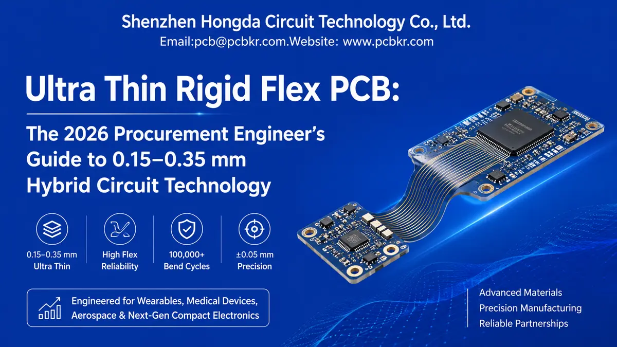
Ultra Thin Rigid Flex PCB: The Procurement Engineer’s Guide to 0.15–0.35 mm Hybrid Circuit Technology
When your product enclosure leaves less than 0.4 mm of vertical clearance, standard rigid-flex PCB stackups stop being an option. Whether you are sourcing boards for AR glasses that fold around a titanium frame, a continuous glucose monitor that must conform to skin curvature, or a CubeSat payload module where every gram determines launch cost, the shift to ultra thin rigid flex PCB technology is not a design preference—it is a structural requirement.
This guide is written for hardware engineers, procurement managers, and product leads who need more than a generic capability sheet. You need to understand what separates a 0.15 mm rigid flex PCB that survives 100,000 dynamic bend cycles from one that delaminates after the first reflow pass. You need to know which manufacturing technologies actually matter in 2026, how to verify them during a factory audit, and where hidden costs hide before you issue a purchase order.
At Shenzhen Hongda Circuit Technology Co., Ltd., we have produced ultra-thin hybrid circuits since 2010. Our Baoan facility runs a 2026-capable equipment line including SCREEN Ledia LDI systems, Mitsubishi UV/CO₂ hybrid laser drilling, and LAUFFER vacuum lamination presses. This article draws from that production data—no marketing fluff, only what we have measured on actual panels.
What Is an Ultra Thin Rigid Flex PCB? Defining the 0.15–0.35 mm Category
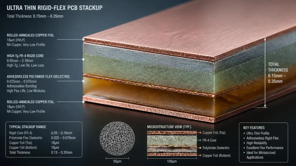
Typical 0.15–0.35 mm Ultra Thin Rigid-Flex PCB Layer Stackup Architecture
An ultra thin rigid flex PCB integrates rigid FR-4 or high-Tg substrate zones with flexible polyimide (PI) sections in a single laminated structure, with a total finished thickness between 0.15 mm and 0.35 mm. That is roughly 30–60 % thinner than conventional rigid-flex boards, where rigid sections typically sit at 0.8–1.6 mm and flex cores at 0.1–0.2 mm.
The thickness reduction is not achieved by simply sanding down a standard board. It requires a fundamentally different material stackup:
| Zone | Conventional Rigid-Flex | Ultra Thin Rigid Flex PCB |
| Rigid core | 0.8–1.6 mm FR-4 | 0.2–0.6 mm high-Tg FR-4 or thin-core laminate |
| Flex dielectric | 25–50 μm PI with acrylic adhesive | 12.5–25 μm adhesiveless PI |
| Flex copper | 35 μm (1 oz) ED copper | 18–35 μm RA (rolled annealed) copper |
| Coverlay | 25–50 μm PI + adhesive | 12.5–25 μm PI coverlay, adhesiveless |
| Total rigid zone | 1.0–1.8 mm | 0.3–0.6 mm |
| Total flex zone | 0.15–0.25 mm | 0.08–0.15 mm |
The move to adhesiveless polyimide is the critical enabler. By eliminating the 12–25 μm acrylic adhesive layer between copper and PI, we reduce the flex zone thickness by roughly 30 % and improve peel strength by 20–40 %, depending on the copper type. In our production line, adhesiveless laminates have become the default for any build below 0.25 mm total thickness.
Why Standard Rigid-Flex Suppliers Struggle Below 0.4 mm
Most PCB factories can quote rigid-flex work. Fewer than 15 % of China-based manufacturers, in our audit experience, can reliably hold ±0.05 mm thickness tolerance on a 0.2 mm flex zone across a 24 × 18 inch production panel. The failure modes are predictable: resin bleed from rigid prepregs into the flex wings, asymmetric copper distribution causing warp, and laser drilling positional drift on unsupported thin cores.
If you are evaluating a thin rigid flex circuit board supplier, ask for cross-sectional micrographs of their last five 0.2 mm or thinner builds. If they cannot produce them within 24 hours, they are not running these boards in volume.
Engineering Specifications & Material Architecture for Ultra Thin Rigid Flex PCB Stackup Design
The Adhesiveless PI Decision
For dynamic bending applications—smartwatch hinges, foldable phone axes, wearable sensor straps—we specify adhesiveless polyimide with RA copper on the flex layers. RA copper has a columnar grain structure that withstands cyclic fatigue far better than electrodeposited (ED) copper, which fractures along grain boundaries after 5,000–8,000 bend cycles.
In static bend applications, such as a medical patch that flexes once during installation and then remains fixed, ED copper on adhesiveless PI is acceptable and reduces material cost by approximately 12 %.
No-Flow Prepreg: The Transition Zone Gatekeeper
The most common defect we see in incoming designs from new customers is the use of standard-flow FR-4 prepreg in the rigid-to-flex transition area. During lamination at 180–200 °C, standard prepreg resin flows 3–5 mm into the PI flex zone, effectively creating a rigid “resin dam” that raises local stiffness by 200 % and destroys bend performance.
Our process mandates no-flow or low-flow prepreg (1080 or 106 glass style) with a resin flow distance under 1.5 mm. We pair this with a stainless-steel lamination fixture that dams the flex window during pressing. The result is a clean transition with no measurable resin intrusion, verified on every first article by cross-section.
Symmetry Rules for Warp Prevention
An ultra thin rigid flex PCB is inherently asymmetrical—FR-4 on one side, PI on the other. Without deliberate stackup balancing, the panel warps toward the rigid side during cool-down. Our DFM protocol enforces:
- Mirror copper weights across the neutral axis, within a 2:1 ratio (e.g., 0.5 oz vs. 1 oz is acceptable; 0.5 oz vs. 3 oz is not).
- Balanced dielectric thickness within 15 % between top and bottom halves of the rigid section.
- Dummy copper mesh fill on sparse signal layers to equalize coverage area and prevent localized stress concentrations.
On a recent 6-layer + 2-flex build for a wearable ECG monitor, these rules reduced post-lamination warp from 0.8 % to 0.25 %—well inside the IPC-6013 Class 3 limit of 0.5 % and the 0.3 % threshold required for safe automated SMT assembly.
Microvia & Fine-Line Capability
Modern ultra-thin wearable and AR devices route MIPI CSI or high-speed differential pairs through the rigid section. That demands microvias and fine lines that do not compromise the thin profile.
Our current production capabilities for ultra thin rigid flex PCB with microvia integration include:
- Laser microvia diameter: 50–100 μm (Mitsubishi UV/CO₂ hybrid laser), with positional accuracy ±5 μm.
- Fine line/space: 20 μm/20 μm in standard production; 8 μm/8 μm qualified on our mSAP (Modified Semi-Additive Process) line for substrate-like builds.
- Impedance control: ±5 % on differential pairs up to 224 G PAM4 equivalent density, verified with in-house TDR.
- Via-in-pad: Supported for BGA pitches down to 0.35 mm, with copper fill and cap plating to eliminate solder voids.
Manufacturing Technology: What Equipment Actually Matters for Ultra Thin Rigid Flex PCB Production

Precision UV/CO₂ hybrid laser drilling microvias on ultra-thin rigid-flex PCB substrate.
Procurement teams often receive glossy equipment lists that mean little without context. Here is what each machine does, why it matters for thin boards, and the measurable outcome you should demand.
Laser Direct Imaging (LDI) — SCREEN Ledia Series
Phototools stretch, shrink, and degrade with humidity. On a 0.2 mm core, a 10 μm misregistration can shift a microvia off its capture pad, creating an open circuit that is invisible until electrical test.
Our SCREEN Ledia LDI system images directly onto resist without a photomask, holding registration at ±1.5 μm. For a 6-layer rigid-flex with 75 μm blind vias, that accuracy ensures the via lands on the 150 μm target pad every time. We have eliminated phototool-related scrap on thin builds since installing this line in Q3 2024.
Procurement verification question: Does your supplier use LDI for rigid-flex, or only for standard HDI? Many factories reserve LDI for high-volume smartphone work and revert to phototools for low-volume rigid-flex, introducing variability.
Hybrid Laser Drilling — Mitsubishi UV/CO₂
Rigid-flex boards require two drilling regimes: mechanical through-holes in the rigid zone, and laser microvias in the rigid-to-flex transition or rigid HDI layers. Our Mitsubishi dual-source system switches between UV (for 50 μm microvias in PI) and CO₂ (for 75–100 μm blind vias in FR-4) without panel transfer.
The critical spec for ultra thin rigid flex PCB LDI manufacturing is not just hole size—it is depth control. On a 0.3 mm total stackup, a 10 μm over-drill punches into the flex core and creates a stress riser. We hold depth tolerance at ±10 μm using real-time energy compensation and CCD alignment.
Vacuum Lamination — LAUFFER Multi-Zone Press
Standard hydraulic presses apply pressure from the top and bottom platens only. On thin panels, this creates edge-to-center thickness variation of ±15 % because the panel bows slightly under pressure.
Our LAUFFER press uses 16 independent thermal zones with real-time pressure feedback. During the 2026 process upgrade, we added AI-driven gradient temperature profiling that ramps at ≤3 °C/min to prevent resin shock, then holds at 190 °C ±1 °C for full cure. The outcome: interlayer delamination rates on 0.25 mm rigid-flex builds dropped from 3.2 % to 0.4 %.
mSAP Fine-Line Processing
For AR glass and camera module applications that need 30/30 μm or finer line/space in the rigid section, subtractive etching fails. The isotropic undercut on 18 μm copper foil creates trapezoidal traces that shift impedance by 2–3 Ω.
Our mSAP line laminates a 2 μm seed layer, images with LDI, plates copper to 18 μm, then flash-etches the seed. The trace sidewalls are near-vertical, enabling 20/20 μm production and 8/8 μm qualification. For a recent 12-layer rigid-flex AR headset board, this held 100 Ω differential impedance within ±4 % across a 500 × 400 mm panel.
AI-Assisted Inspection
We run 3D AOI (Nordson DAGE) on every inner layer and 3D X-ray on all microvia fills. The 2026 upgrade added AI defect classification that flags copper slivers, coverlay misregistration, and microvia voids >5 % with 96 % accuracy. For thin boards where manual inspection risks flexing the panel, automated handling is not optional—it is yield protection.
Application-Specific Design Requirements for Ultra Thin Rigid Flex PCB

Conceptual X-ray view demonstrating ultra-thin rigid-flex PCB routing high-speed signals through a compact AR headset frame.
AR/VR Headsets: Signal Integrity in a 0.18 mm Stackup
AR waveguide drivers route high-speed MIPI signals from the temple-mounted rigid PCB to the display rigid-flex transition. The challenge is not just thickness—it is maintaining 90 Ω differential impedance through a 0.1 mm dielectric with a coverlay on one side and air on the other.
Our solution: Use 3 μm low-profile RA copper on the flex layer, route traces perpendicular to the bend axis, and place ground reference planes on adjacent rigid layers that extend 2 mm into the flex transition. Impedance is verified by TDR on every first article, not just simulation.
Wearable Medical Devices: Biocompatibility & Dynamic Bend Life
A continuous glucose monitor (CGM) patch must survive 14 days of body movement, temperature cycling from 20 °C to 40 °C, and sweat exposure. The flex section bends with every wrist rotation.
We specify: – Adhesiveless PI (DuPont Pyralux AP or equivalent) for moisture resistance. – RA copper with grain direction parallel to the bend axis. – ENIG surface finish (1.5–2.0 μin gold) for wire-bondable biosensor pads. – Dynamic bend testing to 100,000 cycles at a 3 mm radius, per IPC-6013.
Aerospace & CubeSat: Outgassing & Thermal Cycling
Space-grade ultra thin rigid flex PCB for aerospace must pass NASA-STD-6001 outgassing (TML <1.0 %, CVCM <0.10 %) and survive −40 °C to +125 °C thermal cycling without via barrel cracking.
Our AS9100D-certified line uses high-Tg (180 °C+) low-CTE FR-4 for the rigid core, with plated through-holes receiving a minimum 25 μm copper barrel. Every lot receives cross-sectional analysis and thermal shock testing (500 cycles) before shipment.
Foldable Consumer Electronics: The Hinge Zone Problem
Foldable phones place the rigid-flex board across the hinge mechanism, demanding a static bend radius of 1.5 mm or less. The failure mode is copper fatigue at the neutral axis.
We solve this by: – Limiting flex layers to 1–2 in the hinge zone (more layers = larger neutral axis shift = higher strain). – Using teardrop transitions at the rigid-flex boundary to reduce stress concentration. – Adding PI stiffeners (0.05–0.1 mm) on the rigid side of the transition to prevent creasing during the fold motion.
The Procurement Engineer’s Decision Framework: Solving the Five Critical Pain Points
After auditing hundreds of rigid-flex designs, we have identified five failure modes that destroy projects before they reach SMT. Here is how we address each one.
Pain Point 1: Warpage That Kills SMT Yield
The symptom: Your 0.25 mm board arrives flat, but after the first reflow pass it bows to 0.6 %, causing BGA solder opens and tombstoning on 0201 passives.
Root cause: Asymmetric copper distribution or unbalanced dielectric. The thin panel has no structural stiffness to resist thermal stress.
Hongda solution: Every incoming design receives a DFM warpage simulation before tooling. We enforce copper balance rules, recommend dummy fill patterns, and for critical builds, run finite-element analysis (FEA) on the stackup. Post-lamination, panels are baked at 150 °C for 4 hours to relieve residual stress before routing. Final warp is guaranteed <0.3 % for SMT-ready boards.
Pain Point 2: Resin Bleed Into the Flex Zone
The symptom: The flex section feels stiff, fails bend testing, or shows white stress lines at the transition.
Root cause: Standard-flow prepreg resin migrating into the PI area during lamination.
Hongda solution: No-flow prepreg with controlled resin flow <1.5 mm, combined with laser-cut stainless steel dams in the lamination fixture. We verify zero resin intrusion on the first article cross-section and maintain that standard through AOI on the coverlay window edge.
Pain Point 3: Dynamic Bend Life Below Specification
The symptom: Your wearable prototype passes bench testing, but field units fail at 2,000–5,000 cycles.
Root cause: ED copper used in a dynamic bend zone, or traces routed parallel to the bend axis (which concentrates strain on a single copper grain boundary).
Hongda solution: We classify every bend zone as static or dynamic during DFM review. Dynamic zones get RA copper with grain direction verified by etch-pit analysis. Traces are routed perpendicular to the bend axis, and we recommend a bend radius ≥6× total flex thickness for static, ≥12× for dynamic. Every production lot for dynamic applications receives sample bend testing to the customer-specified cycle count.
Pain Point 4: SMT Assembly Damage on Ultra-Thin Panels
The symptom: Components shift during pick-and-place, or the panel warps in the reflow oven, creating head-in-pillow BGA defects.
Root cause: The 0.2 mm panel lacks the rigidity to survive standard SMT conveyor handling.
Hongda solution: We supply SMT carrier fixtures matched to your panel outline—typically a 0.8 mm FR-4 frame with vacuum pockets that hold the thin board flat during printing, placement, and reflow. Our PCBA line uses low-pressure nozzles (≤0.3 N) for component placement and a custom reflow profile with peak temperature 235 °C and ramp rate ≤1.5 °C/s to minimize thermal shock. For customers who assemble externally, we provide carrier drawings and reflow profile recommendations as part of the fabrication data pack.
Pain Point 5: Impedance Drift in Thin Dielectrics
The symptom: High-speed channels fail eye-diagram margin testing, even though the stackup matches the simulation.
Root cause: Dielectric thickness variation in ultra-thin cores (±10 % on a 0.1 mm core = ±10 μm) shifts impedance by 5–8 Ω.
Hongda solution: We source thin cores from vendors who guarantee ±5 % dielectric thickness and verify every incoming lot with micrometer mapping. During imaging, LDI compensates for material stretch. Post-etch, we run TDR on coupon strips from every panel, not just the test board. For 100 Ω differential pairs, we hold ±5 % across the panel and ±7 % lot-to-lot.
Supplier Capability Verification: The 12-Point Audit Checklist for Ultra Thin Rigid Flex PCB Manufacturers
Before you place a $50,000 prototype order, verify these capabilities during a factory audit or video inspection:
- LDI imaging for rigid-flex: Can they show a rigid-flex panel running on the LDI line, or only standard boards?
- Laser drilling depth control: Ask for a cross-section of a 0.3 mm total stackup with blind vias. Measure the remaining dielectric below the via.
- Adhesiveless PI inventory: Do they stock adhesiveless laminates, or only adhesive-based? (Adhesiveless requires higher-temp lamination and different drill parameters.)
- mSAP or semi-additive capability: For fine-line work, do they have a dedicated mSAP line, or are they etching 30/30 μm traces with marginal yield?
- Vacuum lamination: Is the press hydraulic or vacuum? Vacuum is mandatory for void-free thin builds.
- 3D X-ray for microvia voids: What void percentage do they reject? (We reject >5 %.)
- TDR impedance verification: Is TDR testing performed in-house, or outsourced?
- Dynamic bend testing equipment: Can they run cyclic bend tests to 100,000 cycles, or only static radius gauges?
- SMT carrier design support: Will they design and fabricate assembly carriers, or only supply bare boards?
- Cross-sectional lab: Do they have an in-house metallography lab with automated polishing, or do they send samples out?
- Certification scope: Is their AS9100D/ISO 13485 certification current and covering the specific factory building where your boards will run?
- Traceability system: Can they provide material lot numbers, plating bath chemistry logs, and thermal profile records for your specific job?
At Shenzhen Hongda Circuit Technology, we welcome these questions. Our audit room has live equipment feeds, and we provide cross-sectional photos from previous builds under NDA within one business day.
Cost Drivers & Lead Time Strategy for Ultra Thin Rigid Flex PCB Prototyping
What Drives Cost in Ultra-Thin Builds
- Layer count: Each additional lamination cycle adds 20–25 % processing time and increases registration risk.
- Flex layer copper type: RA copper costs 15–20 % more than ED copper.
- Microvia density: >500,000 holes/m² requires femtosecond laser drilling and slows throughput.
- Testing scope: 100 % four-wire low-resistance testing adds 8–12 % to prototype cost but eliminates field failures.
- SMT carriers: Custom FR-4 carriers for thin boards add NRE but reduce assembly scrap by 30–50 %.
Lead Time Benchmarks
| Volume | Standard Lead Time | Expedited |
| Prototype (5–10 pcs) | 8–12 days | 5–7 days |
| Low volume (50–200 pcs) | 12–15 days | 8–10 days |
| Mid volume (500–2,000 pcs) | 18–22 days | 14–16 days |
Expedited builds bypass the standard queue and run on dedicated prototype lines. Note that for 0.15 mm builds, we do not recommend expediting the first article—rushing lamination cooldown increases warp risk by 40 %.
The Prototype-to-Production Path
We recommend a three-stage validation for new ultra-thin rigid-flex designs:
- Stage 1 — DFM + Stackup Review (2–3 days, no cost): We review your Gerbers, flag transition-zone risks, and propose material alternatives.
- Stage 2 — First Article (5–10 pcs): Full cross-section, TDR, bend test, and SMT carrier trial.
- Stage 3 — Pilot Run (50–100 pcs): Process capability study (Cpk) on critical dimensions, establishing control limits for volume.
Skipping Stage 2 to save two weeks typically costs six weeks in rework when the first production lot fails assembly.
Frequently Asked Questions: What Procurement Teams Google Before Sourcing Ultra Thin Rigid Flex PCB
How thin can a rigid flex PCB be manufactured without sacrificing reliability?
The practical limit for volume production is a 0.08–0.10 mm flex zone and 0.15–0.20 mm rigid zone, with total stackups as low as 0.15 mm. Below 0.10 mm flex thickness, handling yield drops sharply—panels tear during conveyance, and coverlay registration drifts. At Shenzhen Hongda, our validated minimum for production volumes is 0.10 mm flex / 0.20 mm rigid, with 0.08 mm flex available for qualified medical and aerospace programs under special handling protocols.
What is the difference between RA copper and ED copper in ultra thin rigid flex PCB, and which should I specify?
RA (rolled annealed) copper is formed by mechanically rolling and heat-treating copper ingots, producing a columnar grain structure that withstands repeated bending. ED (electrodeposited) copper is plated onto a drum, creating a rougher, more brittle surface. For dynamic bend zones (wearables, foldable phones), specify RA copper. For static rigid zones where the board never bends after installation, ED copper is acceptable and less expensive. In hybrid builds, we often use RA on flex layers and ED on rigid outer layers to optimize cost and reliability.
How do I prevent warpage during SMT assembly of a 0.2 mm rigid flex PCB?
Three controls are mandatory: (1) a rigid SMT carrier fixture with vacuum hold-down that matches your panel outline; (2) a balanced stackup with <30 % copper coverage variation between top and bottom layers; and (3) a reflow profile with peak temperature ≤240 °C and ramp rate ≤1.5 °C/s. At Hongda, we supply carrier drawings with every thin-board shipment and can fabricate the carriers in-house if you do not have fixture capability.
What certifications should an ultra thin rigid flex PCB manufacturer hold for medical and aerospace applications?
For medical: ISO 13485 (medical device quality management) and IPC-6013 Class 3 (performance specification for flexible printed boards). For aerospace: AS9100D (aerospace quality) and IPC-6013 Class 3A, plus outgassing test data per NASA-STD-6001 or ESA ECSS-Q-ST-70-02C. For automotive: IATF 16949. Always verify that the certification scope includes the specific manufacturing site, not just a corporate office. Our Baoan facility holds all four certifications with in-scope rigid-flex production.
Why is my rigid flex PCB quote 3× higher than a standard multilayer board of the same layer count?
Rigid-flex requires sequential lamination (rigid and flex sections are processed separately before final pressing), which doubles handling time. Material costs are higher: polyimide is 4–5× the cost of standard FR-4 per square meter, and RA copper carries a 15–20 % premium. Yield loss is higher—thin panels scratch, warp, and misregister more easily. Finally, testing is more extensive: bend testing, cross-sectional analysis, and impedance verification add labor and equipment time. The cost delta narrows at volume (>1,000 pcs) because setup costs amortize, but for prototypes, expect 2.5–4× pricing versus an equivalent rigid board.
Why Shenzhen Hongda Circuit Technology for Your Ultra Thin Rigid Flex PCB Program
We are not a broker. Our 18,000 m² Baoan facility runs rigid-flex production on dedicated lines with equipment we own, maintain, and upgrade. When you email our engineering team, you speak to the same engineers who set the laser drill parameters and review the lamination profiles.
What we offer: – Stackup design review within 48 hours of Gerber submission, with specific recommendations for warp reduction and transition-zone integrity. – First-article validation including cross-sectional micrographs, TDR impedance plots, and dynamic bend test data. – In-house SMT carrier design and PCBA assembly, eliminating the interface risk between fabricator and assembler. – Certified quality systems: ISO 9001, IATF 16949, ISO 13485, AS9100D, IPC-6012 Class 3/3A, UL. – Transparent pricing: Itemized NRE, tooling, testing, and carrier costs—no hidden fees after PO.
Next step: Upload your Gerber files and stackup requirements to PCB@pcbkr.com for a 24-hour DFM review and quote. Or schedule a video factory audit to see our LDI, laser drilling, and lamination lines in operation.
For complex 0.15–0.35 mm rigid-flex projects, we also offer a complimentary 30-minute engineering consultation to review your bend zones, material choices, and SMT strategy before you commit to tooling.
About Author
David Chen https://www.linkedin.com/in/pcbcoming
David Chen boasts an extensive professional background in PCBA manufacturing, PCBA testing, and PCBA optimization, with specialized expertise in high-precision PCBA fault analysis and rigorous PCBA reliability testing. The author has worked with high-layer-count server PCB fabrication, ultra-low-loss backplane stackups, and thermo-mechanical reliability optimization for AI infrastructure projects involving 112G and 224G PAM4 architectures. Skilled in complex circuit design and cutting-edge advanced PCB manufacturing processes, he delivers solutions that elevate product durability and performance across industrial applications. His technical articles focusing on PCBA manufacturing workflows and testing methodologies are widely cited by industry peers, research institutions, and technical platforms, solidifying his reputation as a recognized technical authority in the global circuit board manufacturing sector.