PCB for Power Supply
A reliable PCB for power supply is the foundation of every stable electronic system — and the single largest source of field failures when it is designed or manufactured incorrectly. This guide, written from over a decade of hands-on power supply PCB fabrication and assembly experience at Shenzhen Hongda Circuit Technology Co., Ltd. (www.pcbkr.com), walks engineering and procurement teams through the electrical design fundamentals, the latest manufacturing technologies (heavy copper, insulated metal substrate, copper coin/inlay thermal structures), the biggest pain point in power supply PCB production — balancing current-carrying capacity against thermal reliability without inflating cost or lead time — and the certification and quality-verification steps required before you commit to a manufacturing partner. Every technical recommendation is cross-referenced against IPC-2221, IPC-2152, IPC-6012, and UL standards so that design engineers and buyers can evaluate claims independently rather than take a vendor’s word for it.
What Is a PCB for Power Supply?
A PCB for power supply is a printed circuit board specifically engineered to convert, regulate, and distribute electrical power — from AC mains or a battery — into the clean, stable voltage rails required by downstream circuitry. Unlike signal-layer PCBs, a power supply PCB must simultaneously manage high current density, heat dissipation, electromagnetic interference (EMI), and voltage regulation accuracy on the same board.
Linear vs. Switching Power Supply PCBs
- Linear power supply PCBs use linear regulators (LDOs) to drop voltage through a series pass element. They are simple, low-noise, and cheap for low-current applications, but inefficient — excess energy is dissipated as heat, which drives up thermal design requirements.
- Switching power supply PCBs (SMPS) use high-frequency switching (via MOSFETs and inductors) to regulate voltage with far higher efficiency, at the cost of added EMI management complexity and layout sensitivity.
The right choice depends on load current, efficiency targets, board space, and EMI budget — a decision that should be made before layout begins, not adjusted after fabrication.
Power Supply PCB Design Fundamentals (Engineering Depth)
Grounding and Power Plane Separation
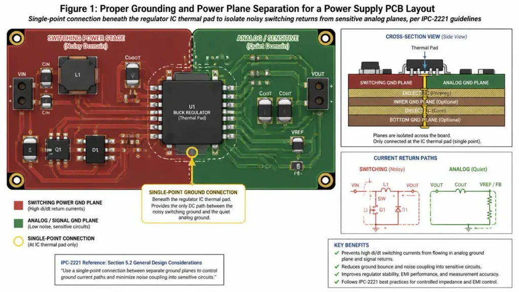
Isolating noisy switching-regulator ground returns from sensitive analog or digital ground planes is one of the most common places power supply PCB designs fail EMC testing. Per IPC-2221 layout guidance, ground planes for power and signal circuits should be split with a single-point connection (commonly a ground via placed beneath the regulator IC’s thermal pad) rather than allowed to share a return path across the board.
Copper Weight and Trace Width for Current Capacity
Trace width and copper thickness are calculated jointly against IPC-2152 (current-carrying capacity of PCB conductors), not IPC-2221’s older static tables alone, since IPC-2152 accounts for board thickness, copper weight, and ambient airflow more accurately. As a working reference:
| Copper Weight | Typical Current Handling (10°C rise, 1mm trace) | Typical Use Case |
| 1 oz (35 um) | ~1.4 A | Control / signal circuits |
| 2 oz (70 um) | ~2.5 A | Light power rails |
| 4 oz (140 um) | ~4.5 A | Standard power supply PCB |
| 6–10 oz (210–350 um) | ~7–13 A | High-current converters, motor drives |
| 20 oz+ (700 um+) | 25 A+ | EV chargers, industrial power modules |
Decoupling Capacitor Placement
0.1 uF ceramic decoupling capacitors should sit within 2–3 mm of each IC’s power pin, with bulk capacitance (10–100 uF) placed nearer the input stage to absorb transient load steps — a detail frequently skipped in beginner-level power supply PCB tutorials but essential for suppressing ground bounce.
Thermal Management for Power Supply PCB Layout
Heat sinks, thermal vias, and forced-air cooling remain standard, but they are no longer the only options available to designers — see the manufacturing technology section below for structural alternatives that eliminate the need for external heat sinks entirely.
Latest PCB Manufacturing Technology for Power Supply Applications
This is where design intent meets manufacturing reality — and where most power supply PCB projects either succeed in production or get stuck in redesign cycles. At Shenzhen Hongda Circuit Technology, our fabrication lines are built specifically around the process capabilities that power electronics demand.
Heavy Copper and Extreme Copper PCB Fabrication
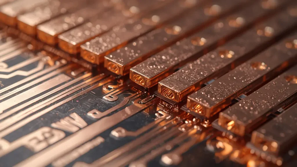
Heavy copper (3–20 oz) fabrication showing thick copper layers and robust busbar structures for high-current power supply applications.
Standard 1 oz copper is inadequate for most power supply applications above a few amps. Modern power supply PCB manufacturing now routinely uses:
- Heavy copper (3–20 oz): reduces conductor resistance and voltage drop while improving mechanical strength around plated through-holes carrying high current.
- Extreme copper (20–200 oz): used in busbar-style embedded power PCBs for EV chargers, industrial converters, and high-power inverters.
Heavy copper fabrication requires differential etching and plating control that standard PCB lines cannot achieve reliably — this is a direct equipment and process-control capability, not a design-file setting.
Insulated Metal Substrate (IMS) and Copper Inlay Technology
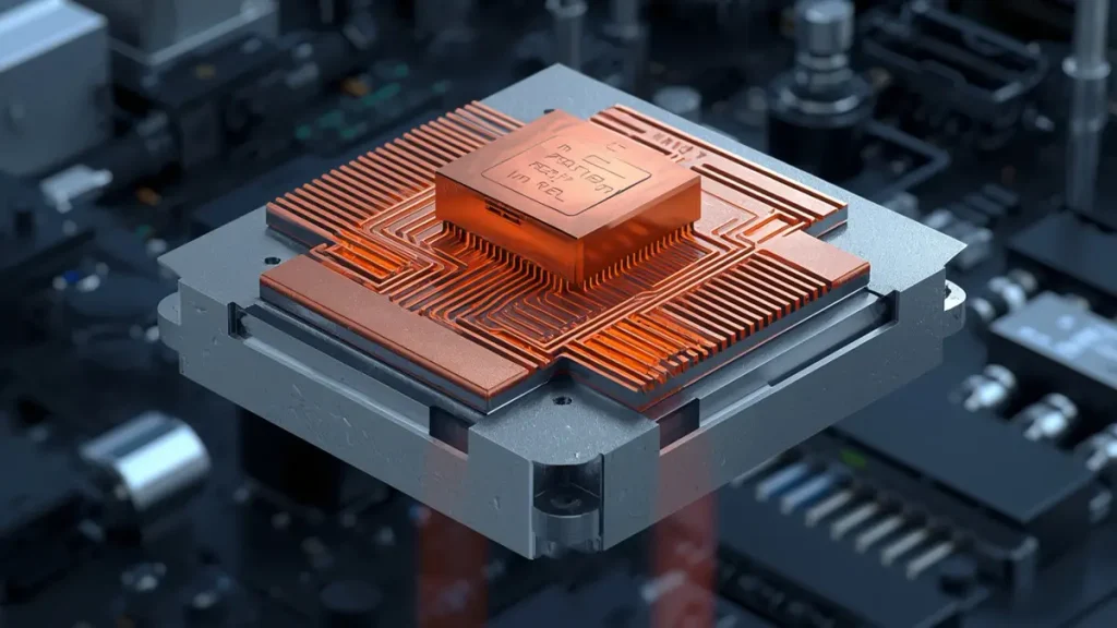
3D cutaway visualization of an Insulated Metal Substrate (IMS) and copper inlay PCB architecture, showing a solid copper coin embedded beneath high-power components to enhance thermal dissipation into the aluminum baseplate.
For power supply PCBs where heat-generating components (MOSFETs, rectifiers, voltage regulators) dominate the thermal budget, insulated metal substrate (IMS) boards use an aluminum or copper base layer with a thin dielectric to conduct heat directly away from the component, replacing bulky external heat sinks.
Copper inlay / copper coin technology goes a step further: a solid copper block is laminated directly into the PCB beneath a high-power component, cutting thermal resistance dramatically compared to thermal vias alone, and simultaneously providing a low-resistance path for high current.
Laser Drilling, LDI Imaging, and AOI/X-Ray Inspection
Precision microvia drilling (laser-based) and Laser Direct Imaging (LDI) allow tighter trace/space geometries on multilayer power supply PCBs without sacrificing registration accuracy — critical when a power plane and a signal plane sit only a few mils apart. Post-fabrication, Automated Optical Inspection (AOI) and X-ray inspection verify copper thickness uniformity, via fill integrity, and hidden solder joint quality on BGA/QFN power ICs — inspection steps that cannot be skipped on boards carrying tens of amps, where a single hairline defect can become a field failure.
How Manufacturing Capability Determines Design Feasibility
None of the layout techniques described above — heavy copper routing, copper inlay thermal paths, tight multilayer registration — matter if the manufacturing line producing the board cannot execute them within tolerance. This is the practical link between design intent and production reality that most generic “power supply PCB design guide” content omits entirely.
The Biggest Pain Point in Power Supply PCB Manufacturing
After ten-plus years fabricating and assembling power supply boards across industrial, LED driver, and telecom applications, the single recurring pain point is this:
Balancing current-carrying capacity against thermal reliability — without inflating cost or lead time.
Increasing copper weight solves current capacity but adds etching time, cost, and lamination complexity. Adding thermal vias or copper inlays solves heat dissipation but adds process steps and drilling precision requirements. Engineers who don’t loop in their manufacturing partner before finalizing the stack-up frequently discover, at DFM review, that their design either:
- Exceeds standard etching tolerance for the specified copper weight, requiring a stack-up redesign, or
- Under-specifies thermal relief around high-power components, risking field failure that only shows up under sustained load — not during initial functional test.
This is precisely why DFM (Design for Manufacturability) review for power supply PCBs should happen at the schematic/stack-up stage, not after Gerber files are finalized.
Choosing a Power Supply PCB Manufacturer
Certifications That Actually Matter
- ISO 9001 — quality management system consistency across production batches
- IPC-6012 / IPC-A-600 — rigid PCB acceptability and qualification standards
- UL certification — required for power supply products sold in markets with safety compliance requirements
- RoHS / REACH compliance — mandatory for most international shipments
(Buyers should request current certificate numbers and verify them directly against the issuing body — a credible manufacturer will provide these without hesitation.)
MOQ, Lead Time, and Cost Drivers for Power Supply PCB Orders
Cost and lead time for power supply PCBs are driven primarily by copper weight, layer count, and whether IMS or copper inlay processes are required — not board size alone. Requesting a quote that separates fabrication cost from assembly (PCBA) cost lets buyers identify exactly where budget is being spent.
RFQ Checklist for Power Supply PCB Quotes
When requesting a quote, include: target current per rail, input/output voltage range, required copper weight, layer count, isolation requirements (if any), certification needs, and expected order volume (prototype vs. mass production).
Frequently Asked Questions About PCB for Power Supply
What is the difference between a linear and a switching power supply PCB?
A linear power supply PCB regulates voltage through a dissipative pass element — simple and low-noise but inefficient at higher currents. A switching power supply PCB regulates voltage through high-frequency switching, achieving much higher efficiency at the cost of added EMI design complexity.
How much copper thickness does a power supply PCB need?
It depends on current load: standard 1–2 oz copper suits low-current control circuits, while 4 oz and above is typical for power supply rails carrying several amps, and heavy/extreme copper (6–20 oz+) is used for high-current converters, motor drives, and EV charging applications.
Why does a power supply PCB overheat?
Overheating is usually caused by insufficient copper cross-section for the current load, inadequate thermal relief around switching components, or missing thermal vias/copper inlay beneath high-power ICs — all of which should be addressed during stack-up design, not after prototyping.
What certifications should a power supply PCB manufacturer hold?
At minimum, ISO 9001 for quality management, IPC-6012/IPC-A-600 for board qualification, RoHS/REACH for material compliance, and UL certification where the end product requires safety compliance.
How long does power supply PCB fabrication and assembly take?
Standard multilayer boards typically ship in 5–7 business days for fabrication; heavy copper or IMS boards, and full PCBA turnkey assembly, generally require longer lead times due to additional etching, lamination, and inspection steps — buyers should confirm lead time separately for fabrication vs. assembly when requesting quotes.
What is copper inlay technology used for in power supply PCBs?
Copper inlay (copper coin) technology embeds a solid copper block directly beneath a high-power component to conduct heat away far more efficiently than thermal vias alone, while also providing a low-resistance current path — commonly used where external heat sinks aren’t practical.
Work With an Experienced Power Supply PCB Manufacturer
Shenzhen Hongda Circuit Technology Co., Ltd. combines the fabrication capabilities described above — heavy copper etching, IMS lamination, copper inlay processing, laser drilling, and AOI/X-ray inspection — with engineering-level DFM review on every power supply PCB order.
Request a quote or DFM review at: https://www.pcbkr.com Email: pcb@pcbkr.com
About Author
David Chen https://www.linkedin.com/in/pcbcoming
David Chen is a Senior RF/PCB Process Engineer at Shenzhen Hongda Circuit Technology Co., Ltd., with over 12 years of experience in high-frequency PCB fabrication, impedance-controlled stack-up design, and Rogers/PTFE laminate processing. He also boasts an extensive professional background in PCBA manufacturing, PCBA testing, and PCBA optimization, with specialized expertise in high-precision PCBA fault analysis and rigorous PCBA reliability testing. The author has worked with high-layer-count server PCB fabrication, ultra-low-loss backplane stackups, and thermo-mechanical reliability optimization for AI infrastructure projects involving 112G and 224G PAM4 architectures. Skilled in complex circuit design and cutting-edge advanced PCB manufacturing processes, he delivers solutions that elevate product durability and performance across industrial applications. His technical articles focusing on PCBA manufacturing workflows and testing methodologies are widely cited by industry peers and technical platforms, and have gained attention and recognition from industry colleagues.