High Precision PCB: Manufacturing, Tolerances, Materials & RFQ Guide
A high precision PCB is a printed circuit board manufactured with tightly controlled line width, spacing, registration, hole position, layer alignment, board thickness, and other dimensional or electrical parameters. The precision level a project actually needs depends on stackup, copper thickness, HDI structure, material selection, application, and production volume — not simply on the smallest feature a manufacturer can claim to produce once. This guide walks engineers and buyers through the parameters, tolerances, materials, manufacturing process, inspection methods, standards, cost drivers, and RFQ requirements behind a high precision PCB, and explains what evidence a qualified high precision PCB manufacturer should be able to provide.
Author: David Chen, Senior PCB Manufacturing Engineer — 12+ years in PCB fabrication, HDI process engineering, and high‑speed PCB reliability testing at Shenzhen Hongda Circuit Technology Co., Ltd. (PCBKR).
What Is a High Precision PCB?
A high precision PCB is defined by dimensional and electrical control across many parameters simultaneously, not by a single “minimum line width” number. In practice, a board is treated as high precision when line width, line spacing, hole position, layer‑to‑layer registration, board thickness, and impedance are all held within tolerances tight enough to guarantee repeatable electrical performance across a production run.
High Precision PCB vs. Standard PCB
A standard PCB typically tolerates wider line/space, looser hole position accuracy, and less stringent registration because the circuit density and signal requirements do not demand it. A high precision PCB is specified because the design margin does not allow for that variation — a few microns of registration drift or a small change in trace width can shift impedance, break a fine‑line net, or cause an annular ring failure.
Precision PCB vs. Fine‑Line PCB, HDI PCB, and High‑Density PCB
These terms overlap but are not interchangeable, and buyers frequently conflate them when writing an RFQ:
| Term | Primary Focus | Typical Driver |
|---|---|---|
| High Precision PCB | Multi‑parameter dimensional/electrical control | Reliability and repeatability at tight tolerance |
| Fine‑Line PCB | Line width/spacing below standard capability | Routing density on a given layer |
| HDI PCB | Microvia and layer‑count density | Miniaturization, BGA escape |
| High‑Density PCB | Overall circuit density | Component packing, layer stackup |
| High‑Reliability PCB | Long‑term field performance | Mission‑critical or harsh‑environment use |
A board can be an HDI PCB without being especially precision‑demanding, and a high precision PCB does not automatically require HDI structures. The two capabilities frequently combine in modern designs, but they answer different engineering questions.
What Makes a PCB “High Precision”?
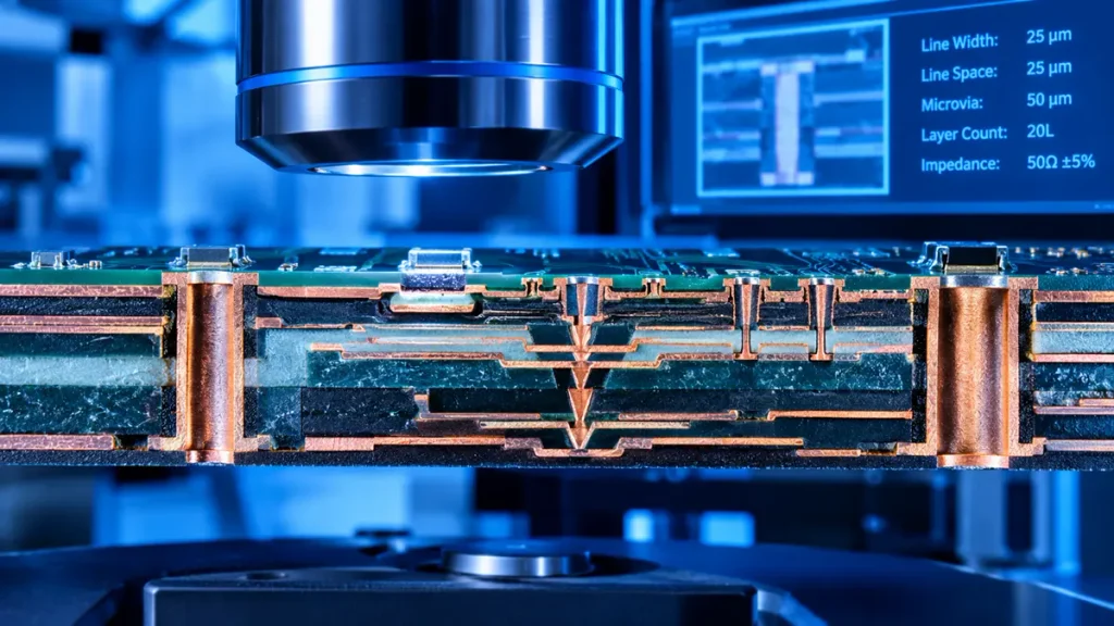
High Precision PCB Cross-Section Analysis Under Laboratory Microscope
The core engineering point is that precision is multi‑parameter control, not a single spec. A manufacturer that only quotes minimum line width is answering a narrower question than the one most buyers are actually asking.
The parameters that collectively define a high precision PCB include:
- Line width and line spacing
- Copper thickness
- Hole diameter and hole position accuracy
- Annular ring
- Layer‑to‑layer registration
- Solder mask registration
- Board outline tolerance
- Board thickness tolerance
- Microvia diameter and depth
- Impedance and impedance tolerance
- Surface finish thickness
- Warpage
- Etching compensation
Reading a High Precision PCB Cross‑Section
Picture a cross‑section of a multilayer board: copper trace and spacing sit on top of a dielectric layer, a microvia connects an outer layer to an inner layer, a plated through‑hole (PTH) passes through the full stack with an annular ring around it, solder mask covers the surface copper, and each layer must register accurately to the ones above and below it. A high precision PCB manufacturer controls all of these simultaneously — not just the smallest trace it can etch on a test coupon.
What PCB Tolerances Matter Most in High Precision Manufacturing?
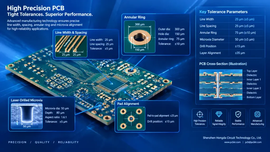
High Precision PCB Manufacturing Tolerances and Microvia Design Guide
Buyers evaluating a high precision PCB manufacturer should look past a single “minimum” number and ask which tolerances are held in mass production, not just in an engineering sample.
Line Width and Line Spacing Tolerance
Nominal design width and finished width are not the same thing. Copper thickness, etching compensation, and whether a trace sits on an inner or outer layer all affect the finished result. Thicker copper requires more aggressive etching compensation, which widens the practical tolerance band and reduces fine‑line yield — a relationship covered in more detail below under copper thickness.
Hole Diameter and Hole Position Tolerance
Mechanical drilling and laser drilling behave differently. Mechanical drilling is generally used for larger PTH/NPTH holes, while laser drilling (CO₂ or UV) is used for microvias. Finished hole size, positional accuracy relative to the pad, and the consistency of hole wall quality after desmear and copper plating all affect whether a design’s annular ring survives lamination movement.
Layer‑to‑Layer Registration
In a multilayer high precision PCB, inner‑layer scaling, lamination movement, and multilayer expansion all shift copper features relative to one another. Registration targets are set to keep those shifts within a range that does not break annular rings or shift controlled‑impedance geometry.
Board Thickness and Outline Tolerance
Finished thickness tolerance interacts with impedance calculations, and outline tolerance affects panelization yield and mechanical fit in the end assembly.
Solder Mask Registration
Solder mask that is misregistered relative to fine‑pitch pads can expose copper or partially cover a pad, both of which create assembly risk on dense BGA and fine‑pitch designs.
Impedance Tolerance
Tight impedance tolerance depends on consistent dielectric thickness, copper thickness, and trace geometry together — it cannot be controlled by trace width alone. This links directly to an Impedance Controlled PCB build, and buyers specifying a high precision PCB for high‑speed signals should treat impedance tolerance as a first‑class requirement, not an afterthought.
What Line Width and Spacing Can High Precision PCBs Achieve?
This is one of the most common search and RFQ questions, and it is also the question most often answered in a misleading way. Typical ranges discussed in the industry span 3/3 mil, 2/2 mil, sub‑2 mil, and µm‑level fine line achieved through SAP (Semi‑Additive Process) or mSAP (modified Semi‑Additive Process), where copper thickness has a direct relationship to how fine a line can be etched cleanly.
Rather than quoting a single minimum number, a high precision PCB capability should be described across three distinct levels:
- Design Target — the line/space value a customer’s design calls for.
- Qualified Capability — a value that has been engineering‑validated on real panels, with documented yield and cross‑section data.
- Stable Mass‑Production Capability — a value that has been demonstrated to hold across repeated production lots, not just a single successful sample.
Many supplier pages list only a minimum line/space figure such as 2/2 mil or 3/3 mil without distinguishing between a one‑time engineering result and a number that repeats reliably at volume. For procurement purposes, the gap between “qualified capability” and “stable mass‑production capability” is often the difference between a design that ships on time and one that stalls in first‑article rejection.
How Does Copper Thickness Affect High Precision PCB Manufacturing?
A common misunderstanding is that fine‑line manufacturing is simply a matter of specifying a thinner trace. In reality, fine line is a function of copper thickness working through the entire etching process:
Copper thickness → etching behavior → sidewall profile → line‑width control → spacing control → impedance → yield.
Thicker copper requires more etching time and more aggressive etching compensation, which degrades sidewall profile and makes tight line/space harder to hold consistently. This creates a direct manufacturing tension between heavy copper requirements (often needed for current‑carrying capacity or thermal management) and fine‑line requirements (needed for routing density). A high precision PCB manufacturer has to manage this trade‑off explicitly in DFM review rather than treating copper weight as an independent line item — a design that specifies both 3 oz copper and sub‑3‑mil line/space on the same layer is asking for two goals that pull the etching process in opposite directions.
How Do HDI and Microvias Improve High Precision PCB Density?
HDI (High Density Interconnect) technology — blind vias, buried vias, microvias, stacked microvias, staggered microvias, via‑in‑pad, and sequential lamination — increases routing density without requiring finer line/space on every layer.
It is worth stating plainly: a high precision PCB is not the same thing as an HDI PCB. A board can require tight dimensional control without any microvia structure, and an HDI board can be built at a moderate line/space if density, not precision, is the primary driver. That said, HDI manufacturing frequently requires high‑precision registration and microvia diameter/depth control to succeed — sequential lamination stacks tolerance on tolerance with each additional lamination cycle, and a registration error introduced early compounds through later stages. In practice, most demanding HDI PCB Manufacturing programs and Microvia PCB or Via‑in‑Pad PCB designs depend on the same registration and dimensional discipline that defines high precision manufacturing more broadly.
Which Materials Are Used for High Precision PCBs?
Material selection for a high precision PCB goes well beyond standard FR‑4.
High‑Tg FR‑4
Used where dimensional stability under thermal cycling is needed but RF‑grade dielectric performance is not required.
Low‑Loss Materials
Materials such as Megtron 6, Megtron 7, and I‑Tera MT40 are used where high‑speed signal integrity and lower dielectric loss matter alongside dimensional precision.
RF and Microwave Materials
Rogers RO4350B, RO4003C, RO3003, RO4450F, and Taconic laminates are common choices for RF and microwave applications where dielectric constant (Dk) and dissipation factor (Df) stability directly affect circuit performance.
PTFE‑Based Materials
PTFE‑based laminates offer strong dielectric stability but bring specific manufacturing considerations: dimensional stability, CTE (coefficient of thermal expansion) behavior, drilling characteristics, lamination process control, and surface treatment before plating all differ from standard epoxy‑based laminates and require process adjustments.
Hybrid Stackups
Hybrid stackups combine two or more material types in a single board — common in high‑speed + high precision PCB designs where only certain layers carry critical high‑speed signals while the rest of the stackup can use lower‑cost material.
How Are High Precision PCBs Manufactured?

High Precision PCB Manufacturing Facility Featuring LDI and AOI Systems
A complete manufacturing sequence for a high precision PCB typically includes:
- Engineering Review DFM analysis against the customer’s stackup, material, and impedance requirements before any panel is started.
- CAM and DFM Translating the design into manufacturing data, including etching compensation and panelization.
- Inner Layer Imaging Applying the circuit pattern to inner‑layer copper.
- LDI (Laser Direct Imaging) Used in place of traditional phototool imaging to improve line‑width accuracy and registration on fine‑line layers.
- Etching Removing unwanted copper to leave the final trace geometry — the step most sensitive to copper thickness, as discussed earlier.
- Registration Control Aligning each layer to the others before and during lamination.
- Lamination Bonding the multilayer stack under heat and pressure.
- Mechanical Drilling Producing larger PTH and NPTH holes.
- Laser Drilling Producing microvias using CO₂ or UV laser systems.
- Desmear Removing resin smear from drilled holes before plating.
- Copper Plating Depositing copper into holes and onto the surface to form electrical connections.
- mSAP / SAP Semi‑additive processes used to achieve finer line/space than standard subtractive etching allows.
- Solder Mask Applying and registering solder mask over the finished copper pattern.
- Surface Finish Applying ENIG, immersion silver, OSP, or another finish depending on assembly and reliability requirements.
- Final Routing Cutting boards to final outline.
- Electrical Testing Verifying continuity and isolation before shipment.
- Sequential lamination is particularly important when manufacturing high-order HDI structures, because each additional build-up cycle introduces another opportunity for registration movement, material shrinkage and microvia alignment errors.
Which Technologies Enable High Precision PCB Manufacturing?
Listing equipment names alone tells a buyer little. What matters is how a specific technology translates into a specific precision outcome. The relationship follows a consistent pattern: Equipment → Process → Precision → Application.
- LDI (Laser Direct Imaging) → removes phototool‑related registration error → tighter line‑width and layer registration → enables fine‑line and HDI layers.
- CCD Optical Alignment → precise layer‑to‑layer alignment before lamination → reduced registration drift → supports high layer‑count multilayer boards.
- CO₂ and UV Laser Drilling → controlled microvia diameter and depth → consistent via reliability → enables HDI and via‑in‑pad structures.
- Picosecond Laser Systems → minimal heat‑affected zone during drilling → cleaner microvia wall quality → supports high‑reliability HDI builds.
- mSAP (modified Semi‑Additive Process) → additive rather than subtractive copper formation → finer achievable line/space → supports sub‑3‑mil and finer routing.
- Sequential Lamination → controlled build‑up of multiple HDI layers → higher interconnect density → enables complex HDI stackups.
- Automated Optical Inspection (AOI) → 100% pattern verification → early defect detection → protects fine‑line yield.
- X‑Ray Inspection → internal via and registration verification → confirms hidden‑layer alignment → supports multilayer and HDI quality control.
- Flying Probe Testing → electrical verification without a dedicated fixture → suited to prototype and low‑volume precision boards.
- 4‑Wire Kelvin Testing → accurate low‑resistance measurement → verifies fine trace and via resistance → supports current‑carrying and thermal validation.
- TDR (Time Domain Reflectometry) and VNA Testing → direct impedance measurement → confirms controlled‑impedance performance → supports high‑speed and RF applications.
This equipment‑to‑outcome mapping is the difference between claiming precision and demonstrating it — a distinction addressed directly in the next section.
How Is High Precision PCB Accuracy Verified?
Competing content frequently repeats phrases like “high precision,” “high quality,” or “strict inspection” without explaining how those claims are actually confirmed. From a procurement standpoint, the real question is: how do you prove it?
- AOI (Automated Optical Inspection) Detects open circuits, shorts, and line‑width deviation across 100% of panels.
- Automated Optical Measurement Quantifies actual feature dimensions against design targets, not just pass/fail defect detection.
- X‑Ray Inspection Verifies internal via alignment, hidden‑layer registration, and void conditions that cannot be seen optically.
- Microsection Analysis Physically cross‑sections a sample to directly measure copper thickness, plating thickness, annular ring, and layer registration.
- Dimensional Inspection Confirms board thickness, outline, and hole position against drawing tolerances.
- Four‑Wire Kelvin Testing Measures fine trace and via resistance with the accuracy needed to catch subtle plating or etching defects.
- TDR Testing Measures actual impedance along a trace to confirm it falls within the specified tolerance.
- VNA Testing Characterizes high‑frequency performance for RF and high‑speed designs.
- SPC / Cpk Statistical process control and process capability index (Cpk) data show whether a parameter is held consistently across many production lots, not just on a single sample.
A supplier’s capability claim carries far more weight when it is backed by inspection data, process capability studies, and production records than when it stands alone as a marketing statement.
Which Standards Apply to High Precision PCBs?
Relevant standards for a high precision PCB manufacturer typically include:
- IPC‑6012 — Qualification and Performance Specification for Rigid Printed Boards
- IPC‑2221 — Generic Standard on Printed Board Design
- IPC‑A‑600 — Acceptability of Printed Boards
- IPC‑4101 — Specification for Base Materials for Rigid and Multilayer Printed Boards
- IPC Class 2 and Class 3, including Class 3A designations where applicable
- ISO 9001 — Quality Management Systems
- IATF 16949 — Automotive Quality Management
- ISO 13485 — Medical Device Quality Management
- AS9100D — Aerospace Quality Management
It is important to separate two different things: certification and dimensional capability are not the same claim. Holding ISO 9001 or IPC Class 3 certification demonstrates a documented quality management system and an acceptance criteria framework — it does not by itself demonstrate that a supplier can hold 2‑mil line/space in mass production. Buyers should request both the applicable certifications and the specific dimensional evidence discussed in the sections above.
How Much Does a High Precision PCB Cost?
Buyers researching high precision PCB cost, fine line PCB price, HDI PCB cost, microvia PCB cost, or precision PCB manufacturing cost should understand that price is driven by a combination of factors, not by the smallest feature alone:
- Layer count
- Board size
- Line/space requirement
- Copper thickness
- Number and type of microvias
- Sequential lamination cycles
- Material selection
- Surface finish
- Impedance control requirements
- Testing scope
- Order quantity
- Expected yield
- Panel utilization
- Engineering complexity
The smallest feature on a design does not determine price by itself. Cost is set by the combination of feature complexity, the number of process steps required, material cost, achievable yield, inspection scope, and production volume together. Two designs with the same minimum line width can carry very different costs if one requires sequential HDI lamination and tight impedance control while the other does not.
How Should Engineers Design for High Precision PCB Manufacturing?
Moving from manufacturing back to design, engineers preparing a high precision PCB layout should account for:
- Minimum clearance requirements
- Annular ring sizing
- Trace width relative to copper thickness
- Via diameter and aspect ratio
- BGA escape routing
- Solder mask clearance and registration allowance
- Impedance‑controlled geometry
- Copper distribution and thermal balance across the panel
- Panelization efficiency
One principle worth emphasizing directly: do not design to a supplier’s absolute minimum capability unless the application genuinely requires it. Designing with margin against the qualified, stable mass‑production capability described earlier — rather than the smallest number a manufacturer has ever achieved once — reduces yield risk and first‑article rejection later in the program.
What Should Be Included in a High Precision PCB RFQ?
A complete high precision PCB RFQ should specify:
- PCB type
- Layer count
- Board dimensions
- Material and Tg
- Dk/Df where relevant
- Finished board thickness
- Copper weight per layer
- Minimum line width/spacing
- Minimum hole size
- Microvia requirements
- Aspect ratio
- Impedance value and impedance tolerance
- Surface finish
- Solder mask type and color
- Required IPC class
- Order quantity
- Prototype quantity
- Mass‑production quantity
- Testing requirements (electrical, impedance, etc.)
- Required inspection reports (AOI, X‑ray, microsection, dimensional)
- Required certifications
- Delivery requirement
An RFQ that includes this level of detail allows a manufacturer to quote against real capability rather than guessing at intent, and it shortens the DFM back‑and‑forth that otherwise delays quoting.
How Should Buyers Evaluate a High Precision PCB Manufacturer?
Rather than searching for “the best manufacturer,” buyers get a more useful result from applying an objective Supplier Qualification Framework:
- Capability Evidence — Does the supplier provide a capability table distinguishing design target, qualified capability, and stable mass‑production capability?
- Process Transparency — Can the supplier explain, step by step, how a specific parameter (line/space, registration, impedance) is controlled through their process?
- Inspection Depth — Does the supplier offer AOI, X‑ray, microsection, dimensional, electrical, and impedance test data as standard deliverables, not optional extras?
- Certification Fit — Do the supplier’s certifications (IPC class, ISO 9001, IATF 16949, ISO 13485, AS9100D) match the end application?
- Prototype‑to‑Production Continuity — Can the supplier demonstrate that a prototype design will hold the same tolerances at production volume?
- Documentation and Traceability — Does the supplier provide material certificates, Certificates of Conformance, and traceability records on request?
This framework is closer to how procurement and quality teams actually make sourcing decisions than a generic “top 10 manufacturers” list, because it evaluates evidence rather than reputation alone.
What Is the Difference Between Prototype and Mass‑Production Precision?
This distinction is one buyers frequently overlook, and it deserves direct attention: prototype capability is not the same claim as mass‑production capability.
A single prototype panel, built with extra engineering attention and a small sample size, can achieve a tighter line/space or tighter registration than the same design will reliably achieve across dozens of production lots. A manufacturer that quotes a minimum capability based on one successful prototype run — without disclosing whether that number holds at volume — is giving buyers an incomplete picture.
| Stage | What Is Being Validated | Typical Sample Size | Risk If Assumed Equal |
|---|---|---|---|
| Prototype | Feasibility of a design target | Small (often single panel) | Overestimates achievable yield |
| Engineering Qualification | Repeatability under controlled conditions | Multiple panels/lots | May not reflect full production variation |
| Stable Mass Production | Consistency across ongoing production | Many lots over time | Represents the realistic delivery baseline |
Buyers moving from prototype to volume production should explicitly ask which stage a quoted capability number represents.
What Applications Require High Precision PCBs?
Precision requirements are not the same across applications, and the reason precision matters differs by use case:
- AI Servers — Fine‑line routing, high layer count, controlled impedance, and tight registration all support signal integrity and power integrity at high data rates.
- High‑Speed Computing — Impedance control and dielectric consistency directly affect signal timing and loss.
- 5G / Communications — RF geometry accuracy and material dielectric stability affect frequency performance.
- Automotive Electronics — Dimensional consistency and reliability support long service life under thermal and vibration stress.
- Medical Electronics — Reliability, dimensional consistency, and full traceability support regulatory and patient‑safety requirements.
- Aerospace & Defense — Reliability and documented process control support mission‑critical performance.
- Radar — Dielectric consistency, impedance control, and RF geometry accuracy directly affect radar signal accuracy.
- RF / Microwave — Material Dk/Df stability and precise geometry affect circuit tuning.
- Industrial Control — Dimensional and electrical consistency support long‑term equipment reliability.
- Semiconductor Equipment — Very tight tolerance requirements support equipment calibration and repeatability.
- Wearables / Miniaturized Electronics — Fine‑line routing and microvia density support compact form factors.
What Are the Most Common High Precision PCB Manufacturing Problems?
Understanding failure modes helps buyers ask better qualification questions:
- Fine‑Line Open Circuits — caused by over‑etching or copper thickness inconsistency.
- Trace Width Variation — caused by inconsistent etching compensation or imaging drift.
- Layer Misregistration — caused by lamination movement or inner‑layer scaling error.
- Via Breakout — caused by insufficient annular ring margin combined with registration drift.
- Annular Ring Failure — caused by hole position error relative to the pad.
- Microvia Reliability Issues — caused by inconsistent laser drilling parameters or desmear quality.
- Resin Void — caused by inadequate lamination pressure or resin flow.
- Copper Thickness Variation — caused by inconsistent plating process control.
- Warpage — caused by material CTE mismatch or uneven copper distribution.
- Impedance Deviation — caused by dielectric thickness or trace geometry variation.
- Solder Mask Misregistration — caused by imaging or alignment drift on fine‑pitch layers.
- Plating Variation — caused by inconsistent current distribution across the panel during plating.
How Can Buyers Reduce High Precision PCB Manufacturing Risk?
From a procurement standpoint, risk reduction comes from specification discipline rather than hoping a supplier “figures it out”:
- Freeze the stackup early in the design cycle.
- Define critical dimensions explicitly rather than leaving them to supplier default.
- Identify which nets require controlled impedance.
- Specify the required IPC class in the RFQ.
- Define the material brand, not just a generic material family.
- Request a DFM review before tooling begins.
- Separate prototype capability requirements from mass‑production capability requirements.
- Request first‑article inspection before full production release.
- Define what inspection evidence will accompany each shipment.
- Establish change‑control requirements for any process or material change.
What Evidence Should a High Precision PCB Manufacturer Provide?
This is one of the most important sections for procurement teams. A qualified supplier should be able to provide, on request:
- A capability table separating design target, qualified capability, and stable mass‑production capability
- Stackup drawings
- Cross‑section and microsection images
- AOI reports
- X‑ray inspection reports
- Dimensional inspection reports
- Impedance test reports (TDR/VNA)
- Cpk/SPC data where applicable
- Material certificates
- Certificate of Conformance (CoC)
- First Article Inspection reports
- IPC compliance documentation
- Traceability records
Do not evaluate precision from a capability number alone. Evaluate the evidence behind the number. A single quoted line/space value means little without cross‑section data, inspection reports, and process capability history to support it.
How Does PCBKR Manufacture High Precision PCBs?
Shenzhen Hongda Circuit Technology Co., Ltd. (PCBKR) builds high precision PCBs around the same evidence‑based process discipline described throughout this guide, rather than treating precision as a marketing label. Precision is engineered and verified at each stage:
- Engineering — DFM review, stackup planning, material selection, and impedance modeling before tooling begins.
- Imaging — LDI‑based imaging for fine‑line pattern control.
- Drilling — Mechanical drilling for standard PTH/NPTH holes, combined with UV and CO₂ laser drilling for microvias.
- HDI Build‑Up — Microvia formation and sequential lamination for high‑density interconnect structures.
- Fine Circuitry — mSAP/SAP processing to achieve finer, more consistent line/space than conventional subtractive etching.
- Inspection — AOI, X‑ray inspection, and electrical testing applied through the production flow, not only at final inspection.
- High‑Speed Validation — TDR and VNA testing to confirm impedance performance on controlled‑impedance boards.
- Quality System — Process control built around IPC standards and ISO‑based quality management practices.
The point of describing the process this way is straightforward: rather than stating “we are a high precision PCB manufacturer,” the goal is to show how precision is engineered and verified at each production stage, so buyers can evaluate the claim against the process behind it — consistent with the Supplier Qualification Framework and evidence checklist described above.
High Precision PCB vs. HDI PCB vs. High Density PCB
| Attribute | High Precision PCB | HDI PCB | High Density PCB |
|---|---|---|---|
| Primary Focus | Dimensional/electrical control across many parameters | Microvia and layer build‑up structure | Overall component and routing density |
| Typical Driver | Reliability and repeatability at tight tolerance | Miniaturization, BGA escape | Component packing on limited board area |
| Requires Fine Line/Space? | Often, not always | Sometimes | Sometimes |
| Requires Microvias? | Not necessarily | Yes, by definition | Not necessarily |
| Requires Tight Registration? | Yes, by definition | Usually, for reliable interconnects | Depends on layer count |
| Typical Application Overlap | Overlaps with both HDI and high‑density designs | Frequently high precision, not always | Frequently precision‑demanding, not always |
High Precision PCB FAQs
What is considered a high precision PCB?
A PCB manufactured with tightly controlled line width, spacing, hole position, registration, thickness, and related dimensional or electrical parameters, sufficient to guarantee repeatable performance across production, not just on a single sample.
What is the minimum line width for a high precision PCB?
Minimum line width varies by process, ranging from roughly 3 mil down to sub‑2 mil or finer with mSAP/SAP, but a meaningful answer distinguishes design target, qualified capability, and stable mass‑production capability rather than quoting one number.
What is the minimum line spacing for a precision PCB?
Line spacing typically tracks line width in similar ranges (for example, 3/3 mil or 2/2 mil), and the achievable value depends heavily on copper thickness and etching process control.
Is a high precision PCB the same as an HDI PCB?
No. A high precision PCB is defined by tight dimensional and electrical control; an HDI PCB is defined by microvia and sequential lamination structure. The two frequently overlap but are not the same requirement.
What PCB tolerances are critical for high precision manufacturing?
Line width/spacing, hole diameter and position, layer‑to‑layer registration, board thickness and outline, solder mask registration, and impedance tolerance are the tolerances most likely to affect yield and reliability.
How accurate can PCB drilling be?
Mechanical drilling accuracy depends on drill bit size, machine calibration, and panel stack height, while laser‑drilled microvias achieve tighter positional accuracy and smaller diameters, typically used for HDI build‑up layers.
What materials are used for high precision PCBs?
High‑Tg FR‑4, low‑loss laminates such as Megtron 6/7 and I‑Tera MT40, RF/microwave materials such as Rogers RO4350B, RO4003C, RO3003, and RO4450F, PTFE‑based laminates, and hybrid stackups combining multiple material types.
What IPC standards apply to high precision PCBs?
IPC‑6012, IPC‑2221, IPC‑A‑600, IPC‑4101, and IPC Class 2/3 (including Class 3A where applicable) are the standards most commonly referenced, often alongside ISO 9001, IATF 16949, ISO 13485, or AS9100D depending on the end industry.
Next Steps
Precision claims are only as useful as the evidence behind them. Depending on where a project stands, PCBKR offers three ways to move forward:
- For Engineers: Send Your PCB Files for Engineering Review
- For Buyers: Request a High Precision PCB Quote
- For Supplier Qualification: Ask for High Precision PCB Capability & Inspection Data
Shenzhen Hongda Circuit Technology Co., Ltd. (PCBKR) | www.pcbkr.com Email: pcb@pcbkr.com
About the Author: https://www.linkedin.com/in/pcbcoming
David Chen is a Senior PCB Manufacturing Engineer with more than a decade of hands‑on experience in PCB fabrication, HDI process engineering, fine‑line manufacturing, and high‑speed PCB reliability testing. His work focuses on connecting design intent to verifiable manufacturing evidence — cross‑section data, inspection reports, and process capability records — rather than capability claims alone.