Smart Meter PCB Manufacturing: How Can OEMs Choose a Reliable Supplier?
Smart meter PCB manufacturing requires more than accurate copper patterns and reliable solder joints. OEMs must control measurement-circuit integrity, electrical isolation, component sourcing, EMC-related design risks, inspection and production traceability. A qualified supplier should review the complete manufacturing package, identify process risks before production, and verify the agreed requirements from prototype through volume manufacturing.
What Is a Smart Meter PCB and Which Manufacturing Requirements Matter Most?
A smart meter PCB supports the metering, processing, power-management, communication and control functions of an electricity meter. Its manufacturing requirements depend on the circuit architecture, rated electrical conditions, measurement design, communication interfaces, applicable standards and expected production volume.
A smart meter may contain several functionally distinct circuit sections:
- Measurement and analog front end: Voltage and current sensing, signal conditioning, reference components and metering ICs.
- Processing and memory: Microcontroller, nonvolatile memory, clock circuitry and related digital interfaces.
- Power management: AC/DC conversion or another specified supply architecture, regulation and protection.
- Communication: Depending on the product, interfaces for cellular, RF, Wi-Fi, Ethernet, optical reading or wired metering networks.
- Control and user interface: Relays, displays, status indicators and external connections.
These functions do not necessarily occupy separate PCBs. Some products integrate the measurement and communication functions on one board; others use multiple boards or plug-in communication modules.
How Do Single-Phase and Three-Phase Smart Meter PCBs Differ?
Single-phase and three-phase meters differ in their sensing channels, input connections, measurement architecture and potential isolation requirements. A three-phase design may require more sensing channels and more complex routing, but its actual PCB layer count cannot be determined from phase count alone.
The manufacturing review should establish:
| Design input | What the PCB supplier needs to confirm |
|---|---|
| Meter architecture | Single-phase, three-phase, direct-connected or transformer-connected |
| Board structure | Dimensions, layer count, finished thickness and stackup |
| Copper construction | Finished copper thickness, current-carrying paths and thermal requirements |
| Electrical safety | Voltage domains, isolation boundaries, creepage and clearance requirements |
| Components | BOM, package dimensions, approved manufacturers and critical components |
| Assembly | SMT, through-hole technology (THT), mixed assembly and special soldering requirements |
| Verification | Electrical tests, functional tests, calibration responsibilities and acceptance criteria |
A common procurement mistake is to send Gerber files without the corresponding fabrication drawing or electrical requirements. Gerber data may describe copper and other manufacturing layers, but it does not necessarily communicate every safety, material, impedance or assembly constraint needed for a complete quotation.
For OEM projects requiring fabrication, assembly or both, begin with the appropriate PCB manufacturing and product capabilities and define the required deliverables before requesting a firm quotation.
Which PCB Materials and Manufacturing Processes Are Suitable for Smart Meter Applications?
FR-4 is suitable for many smart meter designs, but the final material and process must be selected against voltage, temperature, mechanical construction, insulation, copper loading and reliability requirements. HDI and mSAP should be used when the design benefits from their routing density or interconnection capabilities—not simply because they are advanced technologies.
Is Standard FR-4 Enough for Smart Meter PCB Manufacturing?
For many conventional smart meter control and measurement boards, an appropriately specified FR-4 laminate provides a practical balance of cost, mechanical stability and manufacturability.
However, “FR-4” alone is not a complete material specification. The engineering package should identify the required laminate grade, glass-transition temperature where relevant, finished board thickness, copper construction and any applicable flammability or environmental requirements.
The choice should also consider soldering temperature, operating temperature, moisture exposure and the expected service life of the product.
When Do LDI, Laser Drilling and mSAP Improve Manufacturing Capability?https://www.pcbkr.com/advanced-equipment-ai-server-pcb/
PCBKR’s documented manufacturing platform includes SCREEN Ledia laser direct imaging (LDI), Mitsubishi UV/CO₂ laser drilling, LAUFFER lamination equipment and mSAP fine-line processing. Their value depends on the specific design challenge.
| Technology or equipment | Documented capability reference | Relevance to smart meter projects |
|---|---|---|
| SCREEN Ledia LDI | Fine-line process platform; internal capability reference includes 8 µm and approximately ±10 µm positioning | Supports precise pattern imaging and registration where the design requires fine geometry |
| Mitsubishi UV/CO₂ laser drilling | Process reference of approximately 75 µm ±5 µm for applicable microvia structures | Supports laser microvias when routing density and stackup justify HDI |
| Picosecond laser processing | Approximately 50 µm process reference for applicable applications | Specialized precision processing; not a default requirement for ordinary meter boards |
| LAUFFER lamination | Vacuum-assisted lamination; documented operating references include pressures of 80, 150 and 200 psi and vacuum below 50 mbar | Supports controlled multilayer bonding and process consistency |
| mSAP process platform | Qualified internal reference of 8/8 µm line/space for the relevant process route | Enables much finer circuits when the design requires substrate-like interconnection density |
| 3D AOI and X-ray inspection | Complementary inspection methods | Help identify visible assembly defects and selected hidden-joint or internal-structure defects |
These are process-platform references, not guaranteed specifications for every smart meter PCB. Achievable results depend on material, copper thickness, layer count, feature geometry, process sequence and qualification conditions. An 8/8 µm mSAP process is usually unnecessary for a conventional meter controller unless a specific design requirement justifies it.
The procurement implication is straightforward: ask the supplier to identify the least complex qualified process that meets the design requirements. A technically capable supplier should be able to explain when standard multilayer FR-4 is sufficient and when HDI or fine-line processing is warranted.
How Should Copper Thickness and Current-Carrying Paths Be Specified?
Copper weight alone does not establish the safe current capacity of a trace. The required width and copper construction depend on current, allowable temperature rise, copper thickness after processing, surrounding copper planes, airflow, ambient temperature and the physical connections at the trace ends.
For example, a meter design that includes a relay-controlled load path requires different engineering checks from a low-current analog sensing network. The load path may need thermal assessment of traces, terminals, relay contacts and solder joints. The sensing network may instead be more sensitive to leakage, noise coupling and component tolerances.
The supplier should review the specified copper construction and manufacturing constraints rather than independently changing trace geometry to make the board easier to fabricate.
How Can PCB Layout and Assembly Affect Smart Meter Measurement Accuracy?
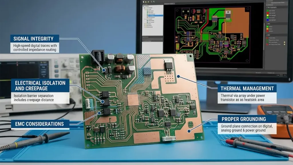
Smart Meter PCB layout and assembly showing measurement circuitry, component placement, and power management
PCB layout and assembly can influence measurement performance through noise coupling, leakage paths, thermal gradients, component placement and solder-joint integrity. Final accuracy also depends on the sensing architecture, metering IC, component tolerances, firmware, calibration and operating environment.
A PCB fabricator cannot guarantee the complete meter’s accuracy merely by meeting dimensional tolerances. The design owner and manufacturing supplier must agree on the boundaries between fabrication quality, assembly verification, functional testing and meter calibration.
How Should Voltage and Current Sensing Networks Be Protected?
The first review should follow the actual measurement signal path from the input or sensor through conditioning components to the metering IC.
The engineer should examine:
- Whether sensitive traces follow the intended routing and reference strategy.
- Whether switching power supplies, relay-drive signals or communication circuits introduce avoidable coupling.
- Whether the specified ground and reference connections are implemented consistently.
- Whether isolation boundaries and high-impedance nodes remain free from unintended copper, contamination or conductive residue.
- Whether component placement and routing follow the metering IC manufacturer’s recommendations.
Engineering note: A recurring design-review risk in mixed-signal boards is treating every ground connection as interchangeable. A board may pass basic continuity testing while still exhibiting unexpected noise or measurement variation because the actual return-current paths differ from the intended circuit behavior. The correct response is to review the schematic, layout and test conditions together—not simply to add copper or enlarge the board.
Why Can Component Substitution Create a Metering Risk?
A procurement team may request an alternative component when a preferred part is unavailable. This can be reasonable for noncritical parts, but substitution should not be treated as a purely commercial decision for precision measurement circuits.
Changes to a reference component, sensing resistor, metering IC or other performance-critical part may affect tolerance, temperature behavior, input characteristics or calibration.
A controlled approval process should include:
- Identification of the original and proposed manufacturer part numbers.
- Review of electrical, mechanical and thermal differences.
- Approval by the customer’s authorized engineering representative.
- Verification testing appropriate to the change.
- Revision and lot traceability for the approved configuration.
An unapproved substitute can turn a seemingly successful assembly into a product-validation problem.
How Should Calibration Be Separated from PCBA Testing?
AOI checks visible assembly features; X-ray can inspect selected hidden joints and internal structures; ICT checks specified electrical nodes; and functional testing checks defined product behavior. None of these automatically establishes the meter’s final measurement accuracy.
The OEM should specify whether calibration is performed by the meter manufacturer, an assembly partner or a separate test facility. If calibration is required, the test procedure should define reference conditions, equipment, limits, data recording and retest criteria.
Which EMC, Electrical Safety and Metering Standards Should Smart Meter PCB Buyers Verify?
The applicable standards depend on the target market, meter architecture and product classification. Buyers should identify the required edition and compliance scope before production rather than assuming that PCB fabrication or PCBA inspection certifies the finished meter.
Relevant references may include:
- IEC 62052-11:2020: General requirements, tests and test conditions for applicable electricity metering equipment. The official IEC description covers functional, mechanical and electrical requirements and immunity to external influences, including electromagnetic and climatic conditions. See the official IEC publication.
- IEC 62053 series: Applicable metering-specific requirements, depending on the meter type and accuracy classification.
- IEC 62052-31: Safety requirements for applicable electricity metering equipment.
- IEC 62056 series: Metering data exchange, including relevant DLMS/COSEM specifications. For example, IEC 62056-5-3:2023 specifies the DLMS/COSEM application layer and communication profiles.
These references have different scopes. The project team must verify the current applicable editions, amendments and regional requirements before making compliance claims.
What Should the Supplier Review for EMC and Electrical Safety?
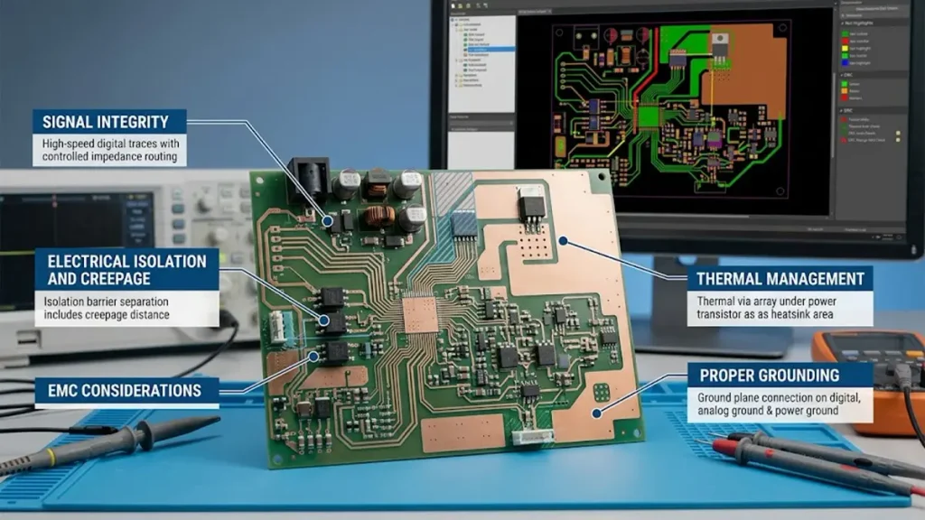
smart-meter-pcb-layout-assembly-measurement-accuracy
Before fabrication, the customer should identify the relevant voltage domains, isolation requirements, interface connections and test conditions.
A useful DFM review includes:
- Creepage and clearance requirements from the approved design and applicable standards.
- Separation of high-voltage and low-voltage circuitry.
- Slots, cutouts or other isolation features where required by the design.
- Solder-mask and exposed-copper requirements at critical boundaries.
- Connector, terminal and relay footprints.
- Grounding, shielding and return-path requirements relevant to EMC performance.
Manufacturing review can identify discrepancies, but it does not replace formal safety analysis, EMC validation or product certification. If a board fails an immunity test, the corrective action may involve the circuit design, enclosure, grounding, filtering or cable configuration rather than a PCB fabrication defect alone.
How Should Smart Meter PCBA Be Inspected and Tested?
Inspection and testing should be selected according to the assembly design, defect risks and agreed acceptance criteria. AOI, X-ray, electrical testing, functional testing and calibration serve different purposes and should not be presented as interchangeable checks.
Which Inspection Methods Are Appropriate?
| Method | What it can help verify | Important limitation |
|---|---|---|
| 3D AOI | Visible component presence, polarity, alignment and selected solder-joint features | Cannot reliably inspect every hidden joint or internal defect |
| X-ray | Selected hidden solder joints, such as BGA connections, and some internal structures | Coverage and defect detectability depend on geometry, materials and inspection settings |
| Flying-probe or ICT | Defined electrical connectivity and test points | Coverage depends on the test program, access and fixture or probing strategy |
| Functional test | Agreed board-level or system-level behavior | Cannot verify requirements that are not included in the test procedure |
| Meter calibration | Measurement performance against specified reference conditions | Requires the appropriate calibration method, equipment and acceptance limits |
PCBKR’s manufacturing equipment references include automated optical inspection, X-ray inspection, electrical testing and high-frequency measurement equipment. These capabilities are useful when matched to a project’s actual risks. For a standard smart meter board, a 70 GHz vector network analyzer is not inherently necessary; it becomes relevant only if the design has suitable high-frequency requirements.
What Manufacturing Defects Should Be Investigated First?
The most useful defect review begins with the observed symptom and traces it back through the manufacturing process.
Scenario 1: The board passes visual inspection but fails functional testing.
Possible causes include an incorrect component value, reversed polarity, a solder defect, a wrong BOM revision or a test setup issue. The team should correlate the failure with component placement, inspection records, electrical test results and the approved design revision.
Scenario 2: A relay or terminal connection shows localized heating.
Review current requirements, terminal and relay ratings, copper geometry, solder-joint quality, component seating and thermal conditions. Increasing trace width alone may not solve a problem caused by a connector or contact resistance.
Scenario 3: Meter readings vary between otherwise similar assemblies.
Review critical component lots, soldering conditions, contamination risks, test-fixture repeatability, firmware and calibration procedures. A manufacturing investigation should separate a genuine assembly variation from differences in measurement conditions.
Scenario 4: Prototype boards work, but pilot production produces intermittent failures.
Compare the prototype and pilot build packages, material lots, assembly profiles, inspection coverage and test procedures. A process that works for a small sample may expose weaknesses when panel utilization, handling, thermal loading or component supply changes.
The key engineering practice is to record the failure mode, reproduce the condition, identify the likely mechanism and verify the corrective action. A vague statement such as “improve quality” is not a sufficient corrective-action plan.
How Do Smart Meter PCB Manufacturers Control DFM and Production Yield?
A reliable process starts with a controlled manufacturing package, identifies fabrication and assembly risks before release, and maintains revision control through prototype, pilot and repeat production.
The DFM review should examine both the bare PCB and the assembled board.
What Should Be Checked Before PCB Fabrication?
- Gerber or ODB++ data against the fabrication drawing.
- Layer count, stackup, finished thickness and copper construction.
- Drill data, annular rings and specified via structures.
- Solder-mask openings, pad geometry and component clearances.
- Isolation features and required electrical spacing.
- Board outline, panelization, tooling and fiducials.
- Controlled-impedance requirements, if applicable.
- Electrical test requirements and acceptance criteria.
For multilayer designs, controlled lamination and registration matter because dimensional changes during processing can affect alignment between layers. PCBKR’s LAUFFER lamination platform and LDI equipment support process control in applicable constructions, but the actual achievable tolerance must be confirmed for the specific stackup.
Which Assembly Risks Commonly Appear During Production?
Small passive components, fine-pitch metering ICs, relays and large connectors can create different assembly challenges. The process review should account for component package, pad geometry, thermal mass, soldering requirements and inspection accessibility.
A common engineering mistake is to approve a PCB layout without considering how it will be inspected and tested after assembly. Test points that are inaccessible, hidden solder joints without an agreed inspection strategy, or connectors that obstruct probe access can increase test development effort and complicate troubleshooting.
The preferred solution is to include DFM, design-for-assembly and design-for-test considerations before the first build, rather than waiting for the pilot run to reveal them.
What Determines Smart Meter PCB Manufacturing Cost and Lead Time?
Total cost and delivery depend on the bare-board construction, component availability, assembly complexity, tooling, test requirements, engineering changes and order quantity. A low bare-PCB price does not necessarily mean a low total manufacturing cost.
| Cost or schedule factor | Why it matters to procurement |
|---|---|
| Board dimensions and panel utilization | Affect material use and the number of boards per production panel |
| Layer count and stackup | Influence material, lamination and process complexity |
| Copper thickness and fine geometry | Can change imaging, etching and plating requirements |
| Surface finish | Affects process cost and suitability for the assembly requirements |
| BOM availability | Can delay assembly or require an approved substitute |
| SMT and THT complexity | Affects setup, soldering, inspection and handling |
| Testing and calibration | May require programming, fixtures, reference equipment and additional time |
| Engineering changes | Can trigger new tooling, material, verification or rework |
| Order quantity | Changes setup-cost allocation and purchasing economics |
How Can Buyers Compare Supplier Quotes Fairly?
Use the same revision, quantity, material specification, assembly scope and test requirements when comparing suppliers. Ask each supplier to identify exclusions, quotation assumptions, nonrecurring engineering charges and component-sourcing responsibility.
For example, Supplier A may quote bare boards only, while Supplier B includes PCB fabrication, component sourcing, SMT, THT and functional testing. Comparing the unit prices directly would be misleading.
The RFQ should also distinguish confirmed lead time from estimated lead time. Component shortages, engineering changes and incomplete test requirements should be documented as schedule risks rather than hidden in a general delivery promise.
How Should OEMs Qualify a Smart Meter PCB Manufacturing Supplier?
Buyers should evaluate a supplier using evidence of relevant manufacturing capability, process controls, quality documentation, traceability and engineering responsiveness. Equipment lists and general quality claims are useful starting points, but they do not replace project-specific qualification.
A practical supplier review should cover five areas:
- Fabrication capability: Confirm materials, layer count, copper construction, minimum geometry and any special processes required by the design.
- Assembly capability: Confirm component packages, SMT/THT scope, sourcing responsibility and inspection methods.
- Testing capability: Review the proposed test plan, test access, fixture ownership, acceptance limits and report format.
- Quality management: Verify current certificates, their scope, applicable sites and any customer-specific requirements.
- Change control and traceability: Confirm how approved BOM revisions, component lots, production records, nonconformances and corrective actions are managed.
PCBKR’s equipment portfolio includes SCREEN Ledia LDI, Mitsubishi UV/CO₂ laser drilling, LAUFFER lamination, automated inspection and electrical test capabilities. The correct qualification question is not whether every advanced process is used on every project, but whether the equipment and process route selected for the specific meter board can meet the approved requirements consistently.
Certification claims must be verified against current certificates and their actual scope. A factory quality-system certificate is not equivalent to certification of a finished electricity meter.
How Can a Smart Meter PCB Project Move from Prototype to Mass Production?
The transition should be managed through a controlled sequence of engineering review, prototype verification, pilot production and formal production release. Each stage should close the issues relevant to the next stage before quantities are increased.
Stage 1: RFQ and Engineering Review
Submit the available PCB data, drawings, BOM, target quantity and test requirements. Identify missing information and obtain agreement on the proposed material, manufacturing scope and acceptance criteria.
Stage 2: DFM and Build-Package Approval
Resolve discrepancies between fabrication data, assembly data and specifications. Approve the component list, revisions, panelization and test approach before production release.
Stage 3: Prototype and Verification
Inspect the manufactured boards and assembled components. Execute the agreed electrical and functional tests, record failures and separate design issues from manufacturing issues.
Stage 4: Pilot Production
Confirm that the approved process can be repeated across the planned pilot quantity. Review defect trends, test coverage, rework, material substitutions and outstanding engineering changes.
Stage 5: Production Release
Approve the production revision, material requirements, test procedures, acceptance criteria and traceability expectations. Changes after release should follow the agreed notification and approval process.
Engineering lesson: A successful prototype demonstrates that a particular build can work; it does not automatically prove that the same result will be repeatable at volume. Production readiness requires controlled inputs, defined process limits and evidence that the verification process can identify relevant defects.
How Can Buyers Request a Smart Meter PCB Manufacturing Quote?
Buyers should provide the files and specifications needed to define the fabrication, assembly, sourcing and testing scope. If some details are unavailable, a preliminary review can identify the information needed for a more accurate quotation.
Include the following wherever applicable:
- Gerber or ODB++ files and drill data.
- PCB fabrication drawing, stackup and laminate requirements.
- Finished board thickness and copper weight.
- Minimum trace/space, hole sizes and any controlled-impedance requirements.
- BOM with manufacturer part numbers and approved alternatives.
- Pick-and-place data and assembly drawings.
- SMT, THT and special process requirements.
- Electrical, functional, calibration and inspection requirements.
- Prototype, pilot and production quantities.
- Target delivery date, destination and packaging requirements.
- Required certifications, traceability records and acceptance criteria.
If the project is still at the design stage, explain which details are provisional. A supplier can then distinguish a preliminary estimate from a firm manufacturing quotation.
Request a Smart Meter PCB and PCBA Quote
Shenzhen Hongda Circuit Technology Co., Ltd. supports PCB manufacturing and PCBA-related projects within its confirmed process scope. Share the available design files and requirements to begin an engineering review.
Email: pcb@pcbkr.com
Website: https://www.pcbkr.com/pcb-products/
Request a review covering manufacturability, assembly requirements, component sourcing, testing scope and the path from prototype to repeat production.
5 FAQs Smart Meter PCB Buyers Ask When Searching for a Supplier
How do I choose a smart meter PCB manufacturer?
Choose a manufacturer whose qualified fabrication and assembly processes match your design. Review its material capabilities, DFM procedure, component controls, inspection methods, test coverage, traceability and relevant quality certificates. Ask for evidence that applies to your specific board rather than relying on general equipment claims.
Can one supplier provide both smart meter PCB fabrication and PCBA assembly?
Some suppliers offer both bare-board fabrication and PCBA assembly, including component sourcing and testing where available. Confirm whether the quotation covers PCB fabrication only, assembly only, partial turnkey or full turnkey service, and identify any excluded tests or outsourced operations.
What files are required for a smart meter PCBA quotation?
Typically, the supplier needs Gerber or ODB++ data, drill files, a fabrication drawing, stackup requirements, a BOM with manufacturer part numbers, placement coordinates and assembly drawings. The test plan, target quantity and delivery requirements help define the full project scope.
How can I reduce smart meter PCBA cost without compromising reliability?
Start with a complete and stable design package, avoid unnecessary layer count or fine-line processing, select materials appropriate to the electrical requirements, and confirm component availability early. Evaluate the total cost of fabrication, assembly, testing, fixtures, approved substitutions and rework—not just the bare-board price.
What should I verify before approving smart meter PCBA mass production?
Verify the approved design revision, material and BOM, DFM closure, assembly inspection plan, functional test procedure, acceptance limits, traceability and change-control process. Review pilot-run results and resolve significant defects before authorizing volume production. Meter calibration and formal product certification should be assigned to the responsible party explicitly.
About the Author
David Chen — PCB Manufacturing and PCBA Engineering LinkedIn Profile
David Chen writes about PCB fabrication, assembly process control, manufacturability, reliability and engineering considerations for OEM procurement. His technical content focuses on connecting design requirements with manufacturing controls and supplier qualification.
Company: Shenzhen Hongda Circuit Technology Co., Ltd.
Website: https://www.pcbkr.com/pcb-products/
Email: sales@pcbkr.com
Technical note: Process figures in this article are capability references, not universal guarantees. Final limits, inspection coverage, standards and test requirements must be confirmed for the actual design, material set and qualified production route.