Looking for a UPS PCB Manufacturer for OEM Production?
Shenzhen Hongda Circuit Technology Co., Ltd. (PCBKR) supports custom PCB manufacturing for demanding electronic applications. For UPS manufacturers, OEMs, and power-electronics buyers, the right production partner must evaluate current-carrying paths, copper thickness, thermal constraints, insulation requirements, fabrication tolerances, and assembly risks before production. Submit your Gerber files, BOM, electrical specifications, and target quantities to request a manufacturing review and project-specific quotation.
What Can a UPS PCB Manufacturer Supply for OEM Projects?
A UPS PCB manufacturer can supply bare printed circuit boards, assembled PCBAs, or an agreed turnkey manufacturing package, depending on the supplier’s verified capabilities and the customer’s requirements. The first step is to identify which board functions and production stages must be outsourced.
An uninterruptible power supply (UPS) may contain several different circuit boards:
- Inverter PCB: Supports the conversion and control circuitry associated with delivering backup power.
- Battery charger PCB: Implements battery charging control and related monitoring functions.
- UPS control PCB: Handles control signals, monitoring, communication, and protection logic.
- Power distribution PCB: Connects power paths and distributes electrical energy between designated sections.
- Bypass and interface PCB: Supports bypass switching, sensing, or external interfaces, depending on the architecture.
These boards do not share identical manufacturing requirements. An inverter power board may prioritize current capacity, heat dissipation, and robust power connections. A control board may place greater emphasis on signal integrity, component density, and separation between high-voltage and low-voltage circuits.
For procurement teams, the distinction between PCB fabrication and PCBA assembly is equally important.
| Procurement model | Typical scope | Information to confirm |
|---|---|---|
| Bare PCB fabrication | Fabrication of unpopulated boards | Gerber files, stackup, copper weight, finish, and tolerances |
| PCB assembly | Component placement and soldering | BOM, centroid file, assembly drawings, and approved parts |
| Turnkey PCBA | Agreed combination of fabrication, sourcing, assembly, and testing | Complete documentation, sourcing rules, test scope, and acceptance criteria |
The exact scope should be documented in the quotation. A supplier should not be assumed to provide system-level UPS testing, firmware development, battery qualification, or complete equipment integration unless those services are explicitly agreed.
Which UPS PCB Specifications Should Buyers Confirm Before Requesting a Quote?
Buyers should define the electrical, mechanical, material, fabrication, assembly, and inspection requirements before requesting a UPS PCB quotation. These inputs determine whether a proposed construction is manufacturable and whether the quoted product matches the intended application.
| Specification | Information required | Why it matters |
|---|---|---|
| Board function | Inverter, charger, control, bypass, or distribution | Establishes the relevant engineering risks |
| Electrical load | Operating voltage, continuous current, peak current, and duty cycle | Determines conductor and connection requirements |
| Copper construction | Starting copper weight and required finished copper thickness | Affects resistance, etching, plating, and cost |
| Layer stackup | Layer count, copper distribution, and dielectric materials | Influences routing, thermal paths, and manufacturability |
| Mechanical design | Board dimensions, thickness, mounting points, and component loads | Affects panelization, warpage, and assembly |
| Thermal conditions | Ambient temperature, allowable temperature rise, and cooling arrangement | Defines thermal design and validation requirements |
| Insulation | Working voltage, transient conditions, and applicable safety standard | Determines clearance, creepage, and dielectric requirements |
| Surface finish | ENIG, HASL, OSP, or another specified finish | Affects solderability, contact requirements, and cost |
| Assembly scope | SMT, through-hole, mixed technology, and component sourcing | Defines production processes and inspection needs |
| Quantity and schedule | Prototype quantity, pilot batch, forecast volume, and target delivery | Affects tooling, setup cost, and production planning |
A nominal power rating alone is not sufficient to select a copper weight or trace width. Engineers need to understand where current flows, how long each conductor is, how heat leaves the board, and whether current transfers between layers through vias or plated holes.
For example, two UPS boards with the same rated power may have very different PCB requirements because one uses short, broad copper paths with effective cooling, while the other routes current through narrow neck-downs, connectors, and multiple layer transitions.
RFQ recommendation: Send the latest released Gerber package, drill files, stackup requirements, BOM, assembly drawings, and any customer-specific acceptance criteria. Identify open design questions rather than allowing a supplier to assume missing requirements.
How Does High-Current UPS PCB Manufacturing Control Copper and Thermal Risks?
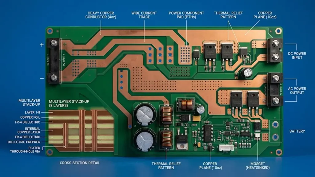
UPS PCB Manufacturer illustrating high-current copper traces and thermal management on a power PCB
Reliable high-current UPS PCB manufacturing requires control of the complete electrical path, including traces, copper planes, pads, vias, plated holes, connectors, and terminals. Increasing copper thickness can reduce conductor resistance, but it cannot compensate for every bottleneck in the design.
How Should Buyers Select Copper Thickness for a UPS PCB?
Common copper weights include 1 oz/ft², 2 oz/ft², and 3 oz/ft². Their nominal copper thicknesses are approximately 35 µm, 70 µm, and 105 µm, respectively. These are nominal conversions; the required finished copper thickness must be specified separately where necessary.
| Nominal copper weight | Approximate copper thickness | Engineering consideration |
|---|---|---|
| 1 oz/ft² | 35 µm | May suit control circuits and some lower-current conductors |
| 2 oz/ft² | 70 µm | May provide lower resistance for suitable power paths |
| 3 oz/ft² | 105 µm | May suit higher-current applications when the design and fabrication process support it |
These values are starting points, not universal recommendations for UPS designs.
Copper resistance depends on conductor length, cross-sectional area, temperature, and material properties. For a simplified conductor, resistance can be calculated as:
R = ρ × L / A
Where:
- R is electrical resistance, measured in ohms (Ω).
- ρ is the electrical resistivity of the conductor material.
- L is the conductor length.
- A is the conductor’s cross-sectional area.
The corresponding first-order relationships are:
Voltage drop: V_drop = I × R
Power loss: P_loss = I² × R
Where:
- V_drop is the voltage drop across the conductor.
- P_loss is the power dissipated as heat.
- I is the current flowing through the conductor.
- R is the conductor’s electrical resistance.
These equations explain why a small resistance increase can become significant in a high-current path. They do not, by themselves, predict the actual PCB temperature, which also depends on conductor geometry, thermal interfaces, airflow, adjacent copper, and the surrounding enclosure.
What Manufacturing Problems Occur with Heavy Copper?
Heavy copper creates a process trade-off that is often overlooked during procurement.
For additional information on heavy copper PCB manufacturing, review the available copper constructions and fabrication considerations. Lateral etching can narrow a conductor or alter spacing. Conversely, insufficient etching can leave unwanted copper and cause shorts. Copper thickness, feature width, spacing, and etch compensation therefore need to be reviewed together.
A second problem occurs at transitions. A wide power plane may feed a much narrower trace, a small pad, a connector pin, or a limited via array. The narrowest or highest-resistance section can become the thermal bottleneck even when the surrounding copper is substantial.
A third problem is mechanical. Uneven copper distribution can affect lamination balance and finished-board flatness. Heavy components, large capacitors, and high-temperature soldering may add mechanical stress during assembly.
For these reasons, a manufacturing review should evaluate:
- Finished copper requirements and the associated etching process.
- Trace neck-downs and current-transfer points.
- Via count, via geometry, and layer transitions.
- Copper distribution, board balance, and finished thickness.
- Connector and component-pad geometry.
- Test access and inspection requirements.
PCBKR’s precision imaging, multilayer fabrication, and inspection technologies can support controlled manufacturing where the design falls within the qualified process window. Final acceptance depends on the actual stackup, copper requirements, fabrication tolerances, and approved manufacturing specification.
How Should UPS PCB Manufacturers Address High-Voltage Insulation?
High-voltage UPS PCB insulation must be designed around the actual electrical environment and applicable safety requirements. Clearance, creepage, dielectric materials, contamination conditions, transient voltages, and manufacturing tolerances must be evaluated together rather than reduced to a single generic spacing rule.
Clearance is the shortest distance through air between conductive parts. Creepage is the shortest distance along an insulating surface between conductive parts. The required distances can differ substantially because the electrical environment and surface conditions affect insulation performance.
The engineering review should consider:
- Working voltage and expected transient overvoltage.
- Applicable product safety standards and insulation category.
- Pollution degree, altitude, and environmental exposure.
- Material group and comparative tracking characteristics where applicable.
- Slots, barriers, board edges, and component lead geometry.
- Solder-mask assumptions and whether the applicable standard permits them to be used in the insulation calculation.
- Fabrication and assembly tolerances that could reduce the intended safety margin.
A design that passes a CAD spacing check may still need further review if connector placement, component leads, routing changes, or assembly tolerances reduce the actual separation.
For example, a UPS control board may place low-voltage sensing circuitry near a high-voltage power section. A last-minute connector change or a relocated component can reduce the available clearance. The manufacturer should identify the change during engineering review and obtain approval before altering the released design.
PCB fabrication testing must also be distinguished from product safety certification. A board-level insulation test, when specified, does not automatically certify the complete UPS. The test method, voltage, duration, acceptance limits, and responsible party must be defined by the applicable design and contract.
Which PCB Materials and Stackups Are Suitable for UPS Applications?
The appropriate UPS PCB material and stackup depend on operating temperature, electrical isolation, mechanical loads, copper requirements, soldering conditions, and total cost. Standard FR-4, high-Tg FR-4, and specialized materials should be selected according to the design rather than by assuming that every power board requires a premium laminate.
Standard FR-4 Versus High-Tg FR-4
Standard FR-4 may be appropriate for many commercial UPS control and power boards. High-Tg FR-4 can provide a larger glass-transition-temperature margin for applications that impose demanding thermal exposure or repeated high-temperature processing.
However, Tg is not the same as the maximum permissible continuous operating temperature. Material selection should also consider decomposition temperature, Z-axis thermal expansion, moisture behavior, dielectric performance, and the laminate manufacturer’s recommended processing conditions.
Two-Layer Versus Multilayer Construction
A two-layer board may be suitable when the circuit can accommodate the required power paths, isolation distances, and control routing without excessive congestion.
A four-layer or higher-layer-count construction may provide more routing flexibility and dedicated copper planes. However, adding layers increases material and processing costs and may introduce additional stackup and registration constraints.
A multilayer board does not automatically improve thermal performance. The result depends on copper distribution, thermal vias, component layout, heat-transfer interfaces, and the enclosure.
Choosing the Surface Finish
ENIG, HASL, and OSP are possible finishes for suitable PCB designs. The choice should reflect soldering requirements, component pitch, contact requirements, storage conditions, and the buyer’s acceptance criteria.
For mixed-technology UPS assemblies, the finish must be evaluated alongside through-hole soldering, surface-mount reflow, and any required shelf-life controls.
A useful quotation should identify the laminate family, finished board thickness, layer count, copper specification, surface finish, and any special mechanical or electrical requirements. Generic material descriptions are insufficient when a design depends on a particular laminate grade.
How Can Advanced PCB Manufacturing Equipment Improve UPS Board Quality?
Advanced PCB equipment improves UPS PCB manufacturing when its process capability matches the actual design challenge. Precision imaging, controlled lamination, laser drilling, plating control, automated inspection, and electrical testing can reduce specific manufacturing risks, but equipment specifications alone do not guarantee product reliability.
PCBKR’s manufacturing technology portfolio includes precision imaging, multilayer lamination, laser drilling, and inspection and electrical-test equipment. The relevant process should be selected according to the UPS board’s copper weight, layer count, feature dimensions, via structure, and acceptance criteria.
Precision Laser Direct Imaging
PCBKR uses SCREEN Ledia laser direct imaging (LDI) technology, with reported imaging capability down to an 8 µm feature target and stated process accuracy of approximately ±10 µm under the applicable conditions.
For UPS projects, the practical value is controlled circuit imaging and registration when a design requires fine features, dense control routing, or accurate layer alignment.
An 8 µm imaging figure does not mean that every UPS board should use 8 µm traces and spaces. Heavy-copper power boards commonly require a different feature geometry, and final achievable dimensions depend on copper thickness, resist system, etching process, panel construction, and the qualified process window.
Multilayer Lamination and Vacuum Processing
PCBKR’s LAUFFER lamination equipment supports process configurations reported at 80, 150, and 200 psi, with vacuum below 50 mbar under the applicable operating conditions.
Controlled lamination and vacuum processing can help manage trapped air, bonding quality, and dimensional stability in suitable multilayer constructions. These factors matter when a UPS board contains multiple copper layers, heavy components, or tightly controlled mechanical dimensions.
The specified pressure and vacuum values are equipment-process parameters, not a universal UPS PCB recipe. The actual lamination cycle must be selected according to the laminate system, copper distribution, stackup, and material supplier’s processing requirements.
Laser Drilling and Via Formation
PCBKR’s laser-drilling technology includes Mitsubishi UV/CO₂ laser processing, with a reported 75 µm microvia capability under qualified conditions, as well as picosecond laser processing with a reported 50 µm feature capability for applicable processes.
Laser drilling can support fine-pitch interconnections and dense control circuitry where the design requires them. It is not a default requirement for a conventional UPS power board.
For a high-current design, the priority is to confirm the via structure, plated-barrel integrity, current-transfer requirements, and reliability under the intended thermal conditions. Smaller microvias are not automatically better for power delivery.
mSAP and Fine-Line Capability
PCBKR has reported mSAP capability at 8 µm line/space for qualified applications. This process is most relevant when a design requires fine-line routing or high interconnection density.
It should not be presented as a necessary UPS technology. Most UPS power paths need conductor dimensions determined by current, resistance, temperature rise, isolation, and manufacturing cost. Fine-line processes are valuable when they solve a genuine layout or integration problem, not simply because the technology is advanced.
Inspection and Electrical Verification
PCBKR’s reported inspection and test resources include AOI, X-ray inspection, four-wire Kelvin flying-probe testing, and a VNA with capability up to 70 GHz.
Their relevance depends on the product:
- AOI: Supports detection of visible pattern and assembly defects within the inspection system’s coverage.
- X-ray inspection: Can help examine hidden solder joints and internal structures that cannot be verified optically.
- Four-wire Kelvin measurement: Can reduce the influence of lead and contact resistance when measuring suitably accessible low-resistance paths.
- Flying-probe electrical testing: Can verify specified bare-board electrical connections without a dedicated bed-of-nails fixture.
- VNA measurement: Is relevant when a design includes controlled high-frequency interconnects or requires specified RF characterization.
A 70 GHz VNA capability does not imply that every UPS board requires a 70 GHz test. Conventional power circuitry usually needs a different validation plan. Likewise, AOI and X-ray cannot replace the electrical and functional tests required by the approved specification.
The engineering objective is to select the right inspection method for each failure mechanism and document what the test can—and cannot—prove.
How Are UPS PCBs Fabricated, Assembled, and Tested?
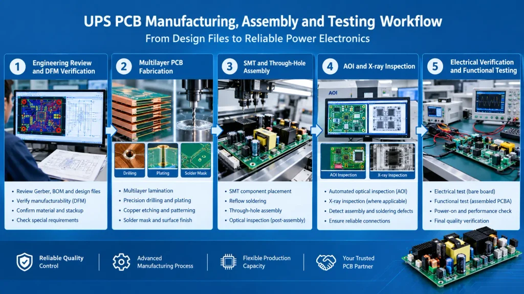
UPS PCB Manufacturer showing PCB fabrication, PCBA assembly, AOI inspection, and electrical testing
A controlled UPS manufacturing workflow links engineering review, bare-board fabrication, assembly, inspection, and agreed electrical verification. Each stage should have defined inputs, process controls, and acceptance criteria.
| Manufacturing stage | Main controls | Typical evidence to agree |
|---|---|---|
| Engineering review | Gerber, stackup, BOM, tolerances, DFM risks | Approved manufacturing data and open-issue list |
| Inner-layer imaging | Feature geometry and registration | Inspection records as specified |
| Etching and copper formation | Trace geometry and copper requirements | Relevant dimensional and copper checks |
| Lamination | Material compatibility, bonding, and board balance | Process records and applicable inspection |
| Drilling and plating | Hole geometry and electrical interconnections | Hole, plating, and electrical inspection as required |
| Solder mask and finish | Pad definition, finish, and solderability requirements | Surface-finish and visual acceptance checks |
| SMT and through-hole assembly | Placement, solder paste, reflow, wave or selective soldering | Assembly inspection and process records |
| Final electrical verification | Defined nets, functions, and acceptance limits | Bare-board test results and/or PCBA test reports |
What Can Bare-Board Testing Prove?
Bare-board electrical testing checks specified connections for opens and shorts. Flying-probe testing is often suitable for prototypes and smaller batches because it does not require the same dedicated fixture as conventional fixture-based testing.
The exact coverage depends on the test program, netlist, accessible test points, and acceptance thresholds. Passing a continuity test does not prove that the board can sustain its rated current indefinitely or that the complete UPS meets its performance requirements.
What Can PCBA Inspection Prove?
AOI can identify many visible assembly defects, including missing or misaligned components, polarity errors within system coverage, and certain soldering defects. X-ray inspection can reveal hidden joint conditions in appropriate packages and structures.
Neither method can establish every electrical or thermal characteristic. Inspection coverage should be tied to the component package, expected defect mechanism, and customer acceptance criteria.
When Is Functional Testing Necessary?
Functional testing should follow an agreed test specification. Depending on the project, this may include power-up behavior, charging control, sensing inputs, communication interfaces, protection logic, or selected operating modes.
Testing a complete UPS under load may require specialized equipment, a safe test setup, a battery or battery emulator, and customer-approved procedures. It must not be assumed to be part of standard bare-board fabrication.
For OEM buyers, the most useful question is not simply whether a supplier offers testing. Ask which defect modes are covered, what the acceptance limits are, which records are retained, and who is responsible for system-level qualification.
What Manufacturing Failures Should UPS PCB Buyers Prevent Before Mass Production?
The most useful failure-prevention strategy connects each plausible defect mechanism to a manufacturing control and a verification method. This is more effective than relying on a general statement that a board has passed inspection.
| Potential failure mechanism | Why it matters | Recommended review or control |
|---|---|---|
| Narrow power-path neck-down | Local resistance and temperature rise may increase | Review conductor transitions and current distribution |
| Inadequate via or plated-hole design | Current transfer may become a bottleneck | Review via geometry, layer transitions, and applicable electrical requirements |
| Heavy-copper etch variation | Actual conductor width may differ from design intent | Verify finished geometry against approved tolerances |
| Uneven copper distribution | May contribute to warpage or lamination challenges | Review copper balance, stackup, and panel design |
| Insufficient insulation spacing | May reduce electrical safety margin | Review creepage, clearance, tolerances, and applicable standards |
| Poor solder-joint formation | Can increase resistance or cause intermittent operation | Define assembly process controls and appropriate inspection |
| Unapproved component substitution | May change electrical, thermal, or mechanical behavior | Require customer approval and component traceability |
| Incomplete test coverage | Some defects may remain undetected | Map each critical requirement to an appropriate test |
Consider a representative engineering scenario: a UPS inverter board passes a visual inspection, but a high-current connection becomes excessively warm during load testing. The correct investigation would not stop at checking the main copper plane. Engineers should inspect the full current path, including pad transitions, via arrays, connectors, solder joints, and any narrow conductors. Four-wire resistance measurements may help locate an unexpected resistive connection when the measurement points and method are appropriate.
This is a general engineering diagnostic approach, not a claim about a documented PCBKR customer failure. Actual root-cause conclusions require measured evidence, the released design, test conditions, and failure-analysis results.
A second scenario involves a board that passes bare-board continuity testing but fails during system integration. Continuity testing can confirm specified electrical connections without proving insulation coordination, dynamic switching performance, thermal stability, or firmware behavior. The investigation must therefore identify whether the failure originates in board fabrication, assembly, design, components, or the system-level test setup.
For procurement teams, this distinction is essential: a reliable supplier should explain the scope and limits of each inspection result rather than presenting a single test as proof of overall product reliability.
How Much Does UPS PCB Manufacturing and Assembly Cost?
UPS PCB manufacturing cost depends on board construction, copper weight, dimensions, materials, process complexity, quantity, assembly requirements, component sourcing, inspection, and delivery schedule. A meaningful quotation must distinguish bare-board cost from the cost of a complete assembled PCBA.
The main cost drivers include:
- Layer count and stackup: More layers typically require additional materials and processing stages.
- Copper weight: Heavy copper can increase etching difficulty and process-control requirements.
- Board thickness and dimensions: Nonstandard constructions may affect material usage, handling, and panel utilization.
- Special processes: Laser-drilled microvias, complex sequential lamination, or fine-line processing add cost when required.
- Surface finish: The finish must match the design, assembly process, and procurement specification.
- Assembly complexity: Component count, fine-pitch packages, through-hole parts, and mixed-technology assembly affect labor and process planning.
- BOM sourcing: Component availability, lifecycle status, minimum order quantities, and approved substitutions influence cost and lead time.
- Testing and documentation: Dedicated fixtures, functional testing, special inspection, and additional reports may require separate quotation.
- Order quantity: Engineering and setup costs are distributed differently across prototypes, pilot batches, and production orders.
A buyer can reduce avoidable cost by supplying complete and consistent manufacturing data, avoiding unnecessary tolerance requirements, and identifying mandatory versus optional testing before quotation.
However, reducing copper weight, insulation spacing, or inspection scope solely to lower cost may create unacceptable engineering or compliance risks. Any proposed cost optimization should be evaluated against the board’s electrical requirements and approved by the responsible design authority.
PCBKR can assess the submitted construction and requirements to determine which manufacturing options are technically appropriate and commercially practical. Final pricing and delivery commitments should be based on the actual project files, quantity, component sourcing requirements, and agreed test scope.
How Can OEM Buyers Qualify a UPS PCB Manufacturing Supplier?
OEM buyers should qualify a UPS PCB supplier by matching the supplier’s actual process capabilities to the design, verifying quality evidence, and establishing clear responsibility for fabrication, assembly, testing, and changes.
Use the following checklist during supplier evaluation:
- Can the manufacturer process the specified copper weight, layer count, material, board thickness, and feature geometry?
- Does the supplier review the complete current path, including pads, vias, connectors, and layer transitions?
- Can it identify manufacturing risks involving heavy copper, registration, warpage, and insulation spacing?
- Are the inspection methods appropriate for the board’s expected failure modes?
- Are test coverage and acceptance limits documented?
- Can the supplier provide the agreed inspection and electrical-test records?
- Are component substitutions subject to an approval process?
- Can material lots, production batches, and engineering changes be traced to the level required by the contract?
- Are prototype, pilot-run, and mass-production conditions clearly stated?
- Are quotation exclusions, tooling costs, delivery assumptions, and warranty responsibilities documented?
What Quality Documents Should a Buyer Request?
The applicable evidence depends on the contract, product classification, and customer quality requirements. Buyers may request relevant inspection reports, electrical-test results, material declarations, batch identification, and documented change control.
IPC-6012 concerns performance and qualification requirements for rigid printed boards, while IPC-A-600 provides acceptability criteria for printed boards. IPC-A-610 addresses the acceptability of electronic assemblies. The applicable revision, class, and contractual requirements should be agreed for the actual product.
A quality-system certificate does not automatically establish that every UPS board meets a particular product standard. Similarly, a manufacturer’s equipment list is not a substitute for evidence that the specified process is qualified for the requested construction.
For high-reliability projects, define the required documentation before production rather than asking for additional evidence after the boards have been manufactured.
How Can You Request a UPS PCB Manufacturing Quote from PCBKR?
To request a UPS PCB quotation from Shenzhen Hongda Circuit Technology Co., Ltd., provide the released design files, electrical requirements, manufacturing specifications, target quantity, and requested delivery schedule. A complete RFQ allows the engineering and sales teams to evaluate the project more accurately.
Please include the following wherever applicable:
- Gerber files and NC drill data.
- Stackup drawing and finished copper requirements.
- Board dimensions, thickness, material, and surface finish.
- Electrical specifications, including operating voltage and current.
- BOM with manufacturer part numbers and approved alternatives.
- Pick-and-place or centroid file.
- Assembly drawings and polarity information.
- Applicable IPC class, inspection requirements, and test procedures.
- Prototype quantity, pilot quantity, expected production volume, and delivery target.
- Any existing samples, failure-analysis findings, or known DFM concerns.
If the design is still under development, identify which requirements are fixed and which remain open for engineering review. This helps avoid unnecessary redesign work and makes it easier to distinguish a fabrication issue from a circuit-design issue.
Request a UPS PCB Quote
Contact Shenzhen Hongda Circuit Technology Co., Ltd. to discuss your custom UPS PCB fabrication or PCBA assembly requirements.
- Website: https://www.pcbkr.com/
- Email: pcb@pcbkr.com
Send your manufacturing files and target order quantities to request a project-specific review and quotation. Final process capability, testing scope, pricing, and delivery commitments are subject to engineering review and written confirmation.
What Should Buyers Ask When Searching for a UPS PCB Manufacturer?
The following five FAQs address the supplier-selection questions most relevant to OEM procurement.
Can a UPS PCB Manufacturer Provide Both PCB Fabrication and PCBA Assembly?
Yes, a supplier may provide both services if its manufacturing scope supports the required bare-board construction, component sourcing, assembly processes, and inspection. Buyers should confirm whether the quotation covers bare boards only, consigned-component assembly, or turnkey PCBA, and whether functional testing is included.
What Files Are Required to Obtain a UPS PCB Manufacturing Quote?
A typical RFQ package includes Gerber files, NC drill data, stackup and copper specifications, board dimensions, BOM, assembly drawings, and a pick-and-place file when assembly is required. Electrical requirements, target quantities, inspection criteria, and delivery expectations should also be included.
How Do I Choose the Correct Copper Thickness for a UPS PCB?
Copper thickness must be selected according to current, conductor length, allowable voltage drop, temperature-rise limits, cooling conditions, and the complete current path. Nominal copper weights such as 1 oz, 2 oz, and 3 oz are common starting points, but the final specification requires engineering evaluation and confirmation of fabrication capability.
What Tests Should I Require from a UPS PCBA Supplier?
Specify the required bare-board electrical test, assembly inspection, and functional test separately. AOI and X-ray can identify certain manufacturing defects, while electrical and functional tests verify different aspects of the product. The appropriate test plan depends on the design, failure risks, and agreed acceptance criteria.
How Can I Compare UPS PCB Suppliers on Quality, Lead Time, and Price?
Compare suppliers using the same released files and acceptance criteria. Evaluate process capability, material and component sourcing, inspection coverage, traceability, quotation exclusions, and delivery assumptions alongside unit price. Confirm which tests and reports are included, and obtain written commitments for the approved manufacturing scope.
About Shenzhen Hongda Circuit Technology Co., Ltd.
Shenzhen Hongda Circuit Technology Co., Ltd. (PCBKR) provides PCB manufacturing and PCBA-related services for OEM and electronics manufacturing projects. Our engineering approach emphasizes manufacturability review, process selection, documented requirements, and verification appropriate to the design.
For UPS and power-electronics projects, the priority is to align the board construction and manufacturing process with the actual electrical, thermal, mechanical, and quality requirements—not to apply the same PCB technology to every design.
Discuss your UPS PCB project: sales@pcbkr.com | https://www.pcbkr.com/
About Author
David Chen LinkedIn Profile
David Chen is a Senior RF/PCB Process Engineer at Shenzhen Hongda Circuit Technology Co., Ltd., with over 12 years of experience in high-frequency PCB fabrication, impedance-controlled stack-up design, and Rogers/PTFE laminate processing. He also boasts an extensive professional background in PCBA manufacturing, PCBA testing, and PCBA optimization, with specialized expertise in high-precision PCBA fault analysis and rigorous PCBA reliability testing. The author has worked with high-layer-count server PCB fabrication, ultra-low-loss backplane stackups, and thermo-mechanical reliability optimization for AI infrastructure projects involving 112G and 224G PAM4 architectures. Skilled in complex circuit design and cutting-edge advanced PCB manufacturing processes, he delivers solutions that elevate product durability and performance across industrial applications. His technical articles focusing on PCBA manufacturing workflows and testing methodologies are widely cited by industry peers and technical platforms, and have gained attention and recognition from industry colleagues.