How Can You Source a Custom Adapter PCB Manufacturer for Fabrication and Assembly?
A custom adapter PCB connects different connectors, interfaces, pin configurations, or electronic assemblies within a specific device or system. Shenzhen Hongda Circuit Technology provides custom adapter PCB fabrication and PCBA assembly for OEM customers, from prototype and small-batch orders to production requirements. We manufacture according to customer-supplied design files, electrical requirements, and assembly specifications. Send your Gerber files and BOM to sales@pcbkr.com for an engineering review and quotation.
What Is a Custom Adapter PCB?
A custom adapter PCB is a printed circuit board designed to establish an electrical or mechanical connection between two components, connectors, interfaces, or electronic assemblies that cannot connect directly.
Unlike a standard functional control board, an adapter PCB is often designed around a specific compatibility requirement. It may change a connector layout, redistribute signals between different pin configurations, provide a physical interface between two boards, or adapt an electronic package to another connection format.
The actual circuit complexity varies considerably. Some adapter boards contain only copper connections between two connector footprints. Others require signal routing, power distribution, level-shifting components, protection circuits, or additional electronic components specified by the customer.
For OEM procurement, the important consideration is not simply whether a board can be fabricated. The PCB manufacturer must also understand the connector specifications, pin assignments, mechanical dimensions, component requirements, and assembly constraints defined in the project documentation.
PCBKR supports custom PCB fabrication and PCBA assembly based on customer-approved design data. The manufacturing scope can be configured according to the board structure, BOM, assembly drawing, and required inspection criteria.
What Types of Custom Adapter PCBs Can Be Manufactured?
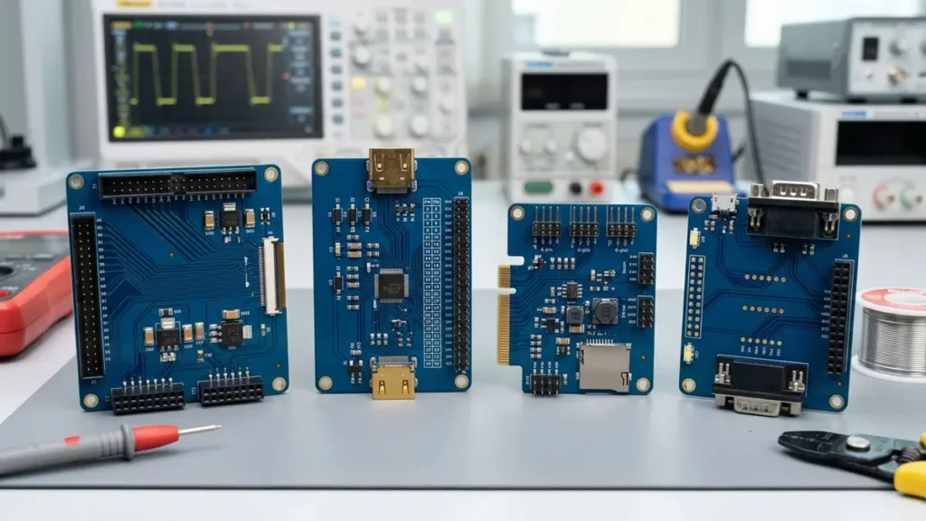
Custom adapter PCB designs for connector compatibility, signal interfaces, and electronic system expansion.
Adapter PCBs are not limited to one connector type or application. Their structure depends on the equipment interface, electronic package, signal requirements, and mechanical connection.
1. Connector Adapter PCB
A connector adapter PCB connects two different connector types or provides a custom connection arrangement between electronic assemblies.
Typical design considerations include:
- Connector series and manufacturer part number
- Pin count and contact pitch
- Pin 1 orientation and pin numbering
- Through-hole or surface-mount termination
- Connector height and mating direction
- PCB outline and mounting-hole locations
Connector compatibility must be verified against the actual component datasheet and approved footprint. A connector with the correct pin count may still be incompatible if its pitch, orientation, mounting pattern, or contact assignment differs.
2. Interface Adapter PCB
An interface adapter PCB provides a physical or electrical connection between two interfaces or electronic subsystems.
Depending on the project, applications may include:
- Board-to-board interface conversion
- Connector arrangement changes
- Equipment interface adaptation
- Control and peripheral connections
- Communication interface connections
Not every interface adapter performs protocol conversion. A passive adapter may only route signals between compatible electrical interfaces. If the project requires active conversion, signal conditioning, or protocol translation, the required components and circuit functions must be defined in the customer’s design.
3. Signal Adapter PCB
A signal adapter PCB routes or reorganizes signals between different connector configurations or circuit sections.
Depending on the signal type, engineering requirements may include:
- Signal assignment and polarity
- Ground reference and return paths
- Trace width and spacing
- Crosstalk control
- Impedance requirements
- Separation between sensitive signals and power circuits
For high-speed applications, the PCB layout must be reviewed against the interface requirements rather than relying on connector compatibility alone.
4. Expansion Adapter PCB
An expansion adapter PCB provides additional connection points or an interface between a main board and peripheral modules.
Its design may involve:
- Additional connector footprints
- Board-to-board connections
- Module mounting arrangements
- Power and signal distribution
- Mechanical clearance for adjacent components
The required layer count, board thickness, copper weight, and material depend on the electrical and mechanical requirements of the application.
5. Package Conversion Adapter PCB
A package conversion adapter PCB allows an electronic component or package to connect to a different footprint or test arrangement.
Examples may include SMD-to-DIP conversion and other package-to-board interface arrangements.
The design must account for the original package footprint, pin assignment, electrical characteristics, soldering method, and the physical dimensions of the target interface. Thermal and signal performance should also be considered where relevant.
What Engineering Requirements Matter in Custom Adapter PCB Design?
The most common manufacturing risks in adapter PCB projects are not necessarily related to complicated circuit structures. They often arise from incorrect connector data, incomplete interface definitions, or mechanical dimensions that have not been checked against the actual equipment.
A reliable manufacturing process starts with the information that defines how the adapter board must connect and operate.
Connector Compatibility and Pin Mapping Verification
Connector compatibility is one of the most important checks before adapter PCB production.
Two connectors may have similar dimensions but different electrical assignments. A footprint can also appear correct in a PCB layout while using an incorrect pin numbering convention or orientation.
Before releasing the design for manufacturing, the following information should be checked:
| Verification Item | What Needs to Be Confirmed |
|---|---|
| Connector part number | Exact manufacturer part number and series |
| Pin count | Number of electrical contacts |
| Contact pitch | Distance between adjacent contacts |
| Pin 1 orientation | Reference direction and numbering |
| Signal assignment | Correspondence between input and output pins |
| Power and ground | Voltage, polarity, and ground allocation |
| Mounting structure | Through-hole, SMT, locating posts, or mechanical supports |
| Mating direction | Horizontal, vertical, or other specified orientation |
A pin mapping table is particularly useful when the two sides of an adapter use different connector arrangements.
For example, the mapping documentation should identify the source connector pin, destination connector pin, and corresponding signal name. Power and ground connections should be identified separately from general signal connections.
The PCB manufacturer should work from the approved design package and raise discrepancies when the supplied information is inconsistent. Functional circuit decisions and electrical pin assignments must remain subject to customer engineering approval.
Mechanical Compatibility Between the Adapter PCB and Connected Devices
An adapter PCB can be electrically correct but still fail during equipment integration if its physical dimensions are inaccurate.
Mechanical compatibility should be reviewed before fabrication, especially when the board must fit inside an enclosure or connect directly to another PCB.
Important dimensions include:
- PCB length, width, and thickness
- Connector center positions
- Connector height and mating clearance
- Mounting-hole diameter and position
- Board edge and cutout geometry
- Component height and keep-out areas
- Clearance from enclosure walls and adjacent assemblies
For board-to-board connections, the relative position of the mating connectors is especially important. A small dimensional deviation can create mechanical stress or prevent reliable mating.
Customers should provide the mechanical drawing, relevant connector datasheets, and any available enclosure or mating-board dimensions when these affect the adapter design.
PCB fabrication tolerances should be agreed according to the drawing and project requirements. They should not be assumed to be identical across all board materials, thicknesses, and manufacturing processes.
Electrical Compatibility and Power Distribution
The adapter PCB must support the electrical requirements of the connected devices.
For simple passive adapters, the main concern may be correct signal routing and connector assignment. For power-carrying or active adapter boards, additional checks may be necessary.
These may include:
- Operating voltage and current
- Copper thickness and conductor width
- Voltage drop and temperature rise
- Clearance and creepage requirements where applicable
- Grounding and return-current paths
- Protection components and polarity
- Isolation requirements, if specified
High-current paths may require wider traces, heavier copper, or an appropriate layer arrangement. The correct design depends on current, allowable temperature rise, copper thickness, board geometry, and the surrounding thermal conditions.
For power-related projects, PCBKR’s PCB for Power Supply page provides additional context on power PCB manufacturing requirements.
Electrical design approval should be completed before production. PCB fabrication alone does not establish that a customer-designed circuit meets its application-level safety or performance requirements.
PCB Fabrication Requirements for Custom Adapter Boards
The manufacturing specification of an adapter PCB should be based on the actual electrical, mechanical, and assembly requirements.
A simple two-connector adapter may use a straightforward PCB structure. A more complex interface board may require multiple layers, controlled impedance, fine-pitch component footprints, or special drilling and routing processes.
The following parameters should be defined in the fabrication package.
| PCB Parameter | Project Requirement |
|---|---|
| PCB material | FR-4 or customer-specified material |
| Layer count | Based on routing and electrical requirements |
| Board thickness | Defined by the mechanical drawing |
| Copper thickness | Selected according to current and design requirements |
| Minimum trace / space | Based on layout density and manufacturing capability |
| Minimum hole size | Based on via and component-hole requirements |
| Surface finish | ENIG, lead-free HASL, OSP, or specified finish |
| Board outline | Based on the approved mechanical drawing |
| Impedance | Controlled only where required by the interface design |
PCB Imaging and Fine-Line Manufacturing
Adapter PCBs with dense connector layouts or fine-pitch components may require accurate imaging and pattern transfer.
PCBKR uses SCREEN Ledia LDI equipment with an 8 μm target imaging capability. Actual achievable conductor geometry depends on the complete manufacturing process, including copper thickness, resist, etching, design rules, and production conditions.
The imaging equipment specification should not be interpreted as a universal minimum trace width or spacing for every adapter PCB. The final manufacturing limits must be confirmed during CAM and DFM review.
Drilling and Via Formation
Via and hole requirements depend on the number of layers, component termination method, board thickness, and routing density.
PCBKR’s manufacturing equipment includes Mitsubishi UV/CO₂ laser drilling with a stated 75 μm ±5 μm capability, as well as picosecond laser processing with a stated 50 μm capability.
These capabilities are relevant when the design requires laser-formed microvias or other precision features. They are not necessary for every standard adapter board.
The final drill structure, aspect ratio, via type, and applicable tolerances must be checked against the actual stackup and fabrication data.
Lamination and Multilayer Construction
Multilayer adapter PCBs may be required when the board needs additional routing space, dedicated ground planes, power distribution, or controlled signal paths.
PCBKR uses LAUFFER lamination equipment with process pressure settings of 80, 150, and 200 psi, and a vacuum capability below 50 mbar.
The correct lamination process depends on the material system, layer construction, copper distribution, board thickness, and other process parameters. These equipment specifications should not be treated as a fixed recipe for every board.
For projects requiring HDI structures or more complex interconnections, review the relevant HDI PCB manufacturing information.
DFM and DFA Considerations for Adapter PCB Assembly
Design for Manufacturability (DFM) and Design for Assembly (DFA) are particularly important for adapter PCBs because connectors often determine how the board is positioned, soldered, inspected, and integrated into the final equipment.
A board may pass PCB fabrication inspection but still present assembly problems if the connector footprint, component spacing, or soldering access is inadequate.
Connector Footprint and Soldering Accessibility
Before assembly, connector footprints should be compared with the approved component datasheets.
The review should consider:
- Pad dimensions and spacing
- Through-hole diameter and plating requirements
- SMT land pattern
- Component body dimensions
- Soldering access
- Mechanical retention features
- Clearance for inspection and rework
Through-hole connectors may require sufficient access for soldering and inspection. SMT connectors may require careful pad design and suitable reflow conditions.
Component Spacing and Assembly Orientation
Adapter PCBs often have limited space around connectors. Component placement should account for connector bodies, mating parts, adjacent components, and the assembly process.
The assembly drawing should clearly identify component orientation, polarity, and reference designators.
For connectors with similar footprints but different orientations, the assembly documentation should be especially clear. An incorrect connector orientation can make the finished board unusable even when the solder joints are acceptable.
Solder Joint Quality and Inspection Access
Inspection requirements should be defined according to the component type and assembly structure.
PCBKR can apply inspection methods such as:
- 3D AOI for applicable visible solder joints and component placement
- X-ray inspection for suitable hidden solder joints
- Electrical testing according to the approved test method and project requirements
AOI does not replace electrical testing, and X-ray is not required for every connector or assembly. The inspection plan should reflect the actual component package, joint visibility, product risk, and customer acceptance criteria.
Custom Adapter PCB Fabrication and PCBA Assembly Process
PCBKR provides PCB fabrication and PCBA assembly according to customer-approved manufacturing files and project requirements.
A typical project can follow the process below.
1. Review of Gerber Files and Technical Requirements
The initial review covers the supplied Gerber files, drill data, stackup, board dimensions, connector specifications, and any special manufacturing requirements.
If the customer provides an assembly package, the BOM, assembly drawing, and placement data are also checked for completeness and consistency.
Questions involving pin mapping, component selection, or circuit functionality should be resolved with the customer’s engineering team before production release.
2. PCB Fabrication
The PCB is manufactured according to the approved fabrication data and agreed specification.
The process may include:
- Material preparation
- Inner-layer imaging, where applicable
- Etching and layer inspection
- Lamination for multilayer boards
- Drilling and via processing
- Plating and outer-layer pattern formation
- Solder mask and surface finish
- Board profiling and final inspection
The actual process route depends on the board construction and manufacturing specification.
3. Component and BOM Review
For PCBA projects, the BOM should identify component manufacturer part numbers, descriptions, quantities, and approved alternatives where applicable.
Connector procurement deserves particular attention. Similar-looking connectors may have different contact arrangements, mounting dimensions, plating, or electrical ratings.
Any proposed component substitution should be reviewed and approved by the customer before assembly.
4. SMT and THT Assembly
Assembly methods depend on the component package and board design.
PCBKR supports SMT and through-hole assembly according to the approved BOM and assembly drawing. Some adapter boards require only connector installation, while others include resistors, capacitors, protection devices, ICs, or other specified components.
The assembly process is configured around the actual component types and soldering requirements.
5. Inspection and Electrical Testing
Inspection and testing are defined according to the product structure and customer requirements.
Available inspection resources include 3D AOI, X-ray inspection, and 4-wire Kelvin flying probe testing.
The appropriate method depends on whether the assembly contains visible solder joints, hidden joints, fine-pitch packages, or accessible electrical test points.
Where a customer requires continuity, isolation, polarity, or functional testing, the test conditions and acceptance criteria should be supplied or approved before production.
6. Final Inspection and Delivery
The completed order is checked against the agreed manufacturing and assembly requirements before delivery.
The delivery scope can be configured as PCB fabrication only or PCB fabrication plus PCBA assembly. Packaging, labeling, test records, and other documentation should be agreed during quotation.
Signal Integrity and Reliability Considerations for High-Speed Adapter PCBs
Not every adapter PCB requires controlled impedance or advanced signal-integrity analysis. However, when an adapter carries high-speed signals, the transition between connectors and PCB traces can affect electrical performance.
The design should be evaluated according to the actual interface data rate, edge rate, connector characteristics, stackup, and routing geometry.
Impedance Control
Where the interface requires controlled impedance, the target impedance should be defined in the design documentation.
The stackup, dielectric properties, copper thickness, trace width, and reference-plane structure all influence the final impedance.
The required tolerance should be agreed before fabrication. It should not be assumed that all adapter boards require the same impedance target.
Signal Return Paths
High-speed signal routing requires a suitable return-current path.
Changes in reference planes, ground discontinuities, and poorly designed transitions may affect signal quality. Connector placement and via arrangement should therefore be considered together with the PCB routing.
Crosstalk and Routing Separation
Adjacent signal traces can couple energy, particularly when they run in parallel over a significant distance or have insufficient separation.
The required spacing depends on signal characteristics, stackup, trace geometry, and the permitted noise level.
Sensitive signals should be routed according to the electrical design requirements rather than applying one universal spacing rule.
Connector Transition and Via Design
The transition from a connector pin to a PCB trace can introduce discontinuities.
For high-speed designs, the layout may need to consider:
- Connector launch geometry
- Via placement and stub length
- Reference-plane continuity
- Return-path transitions
- Differential-pair geometry, where applicable
These considerations should be addressed during design review and confirmed through appropriate simulation or measurement when required by the project.
PCBKR has VNA measurement capability up to 70 GHz. The use of VNA testing, test coupons, or other signal-integrity verification methods should be agreed according to the project’s frequency range, test access, and acceptance criteria.
Custom Adapter PCB Prototype and Mass Production
Prototype approval is an important step before an adapter PCB moves into recurring or volume production.
A prototype should verify not only that the PCB can be fabricated, but also that the connectors mate correctly, the mechanical dimensions fit, and the assembly matches the approved documentation.
Prototype Validation
Depending on the project, prototype checks may include:
- PCB dimensions and hole locations
- Connector part number and orientation
- Pin mapping and continuity
- Component placement and soldering
- Mating compatibility with the target equipment
- Electrical performance against the approved test criteria
The validation plan should be defined by the customer and engineering team. A simple passive adapter may need a different test plan from an active signal-conditioning board.
Moving from Prototype to Production
Before repeat production, the approved revision should be frozen and the manufacturing package checked for consistency.
Important controls include:
- Gerber revision
- BOM revision
- Assembly drawing revision
- Approved component alternatives
- Connector manufacturer part numbers
- Inspection criteria
- Test specifications
A change to a connector, footprint, or pin assignment can affect the entire assembly. Revision control is therefore essential for avoiding unintended differences between prototype and production orders.
Production Consistency
For repeat orders, manufacturing and assembly should follow the same approved documentation and agreed inspection criteria.
Panelization, component availability, board handling, connector positioning, and test access may influence production planning.
The appropriate batch size and production schedule depend on board complexity, material availability, component lead time, assembly requirements, and order quantity. A fixed delivery time should only be confirmed after reviewing the actual project files.
What Affects Custom Adapter PCB Manufacturing Cost and Lead Time?
The cost of a custom adapter PCB is determined by its complete manufacturing and assembly scope rather than by board dimensions alone.
Two boards with similar outlines may have significantly different costs if they use different connectors, layer counts, materials, assembly methods, or testing requirements.
| Cost Factor | How It Affects the Project |
|---|---|
| Board dimensions | Influences material utilization and panelization |
| Layer count | Affects PCB construction and process complexity |
| Material | Special materials may increase material and processing costs |
| Copper thickness | Can affect etching, plating, and conductor requirements |
| Hole and via structure | Fine drilling or HDI features may require additional processing |
| Surface finish | Depends on component and application requirements |
| Connector selection | Special or high-cost connectors can increase BOM cost |
| Assembly method | SMT, THT, and mixed assembly have different process requirements |
| Component sourcing | Availability, MOQ, and lead time affect purchasing |
| Testing | Additional electrical or functional tests require defined procedures |
How to Reduce Quotation Delays
A complete RFQ package helps the manufacturer assess the project more accurately.
To avoid unnecessary clarification, buyers should provide:
- Latest Gerber files and drill data.
- PCB fabrication specifications.
- BOM with manufacturer part numbers.
- Assembly drawing and placement data.
- Connector datasheets and pin mapping.
- Required quantity and expected order frequency.
- Testing and inspection requirements.
- Target delivery date and destination.
If some information is not yet available, identify the missing items in the RFQ. The manufacturer can then clarify which details are necessary before quotation or production.
What Should Buyers Include in a Custom Adapter PCB RFQ?
When sourcing a custom adapter PCB manufacturer, procurement teams should provide enough information for the supplier to evaluate fabrication, component procurement, assembly, and testing requirements.
The following checklist can be used when preparing an RFQ.
| RFQ Information | Recommended File or Details |
|---|---|
| PCB design | Gerber RS-274X or accepted manufacturing data |
| Drill information | Excellon drill files |
| PCB specification | Layer count, material, thickness, copper weight |
| Board dimensions | Outline drawing and mechanical dimensions |
| BOM | Manufacturer part number, quantity, approved alternatives |
| Assembly information | Assembly drawing and Pick-and-Place data |
| Connector details | Datasheet, footprint, part number, mating information |
| Pin mapping | Signal correspondence between interfaces |
| Electrical requirements | Voltage, current, signal type, impedance if applicable |
| Testing | Continuity, isolation, functional, or other defined tests |
| Order information | Prototype quantity, production quantity, delivery schedule |
PCB Fabrication Only or Complete PCBA Assembly?
The required supply scope should be clearly identified in the RFQ.
PCB Fabrication Only
The supplier manufactures bare adapter PCBs according to the approved Gerber files and fabrication specifications.
PCB Fabrication + PCBA Assembly
The supplier manufactures the bare boards and assembles the customer-specified components according to the BOM and assembly drawing.
PCBKR supports both project scopes. The final quotation depends on the supplied files, component requirements, assembly method, inspection plan, and order quantity.
Request a Custom Adapter PCB Quotation from PCBKR
Shenzhen Hongda Circuit Technology Co., Ltd. provides custom PCB fabrication and PCBA assembly for OEM customers requiring different adapter board structures and interface configurations.
To request a quotation, send the available project files and specifications to:
Email: sales@pcbkr.com
Website: www.pcbkr.com
For a faster engineering review, include the Gerber files, BOM, connector datasheets, pin mapping, required quantities, and target delivery schedule.
PCBKR will review the supplied manufacturing information and clarify any missing details needed to evaluate the project scope.
Frequently Asked Questions About Custom Adapter PCB Manufacturing
What types of custom adapter PCBs can a manufacturer produce?
A manufacturer can produce different adapter PCB structures according to the customer’s design, including connector adapter boards, interface adapter boards, signal adapter boards, expansion adapter boards, and package conversion boards. The actual manufacturing scope depends on the PCB files, connector specifications, electrical requirements, and assembly details.
What files are required to manufacture a custom adapter PCB?
A typical RFQ should include Gerber files, drill data, PCB specifications, BOM, assembly drawing, and Pick-and-Place data when assembly is required. Connector datasheets and pin mapping information are also important when the board connects different interfaces. Additional electrical or mechanical drawings may be needed for specialized applications.
Can PCBKR provide both custom adapter PCB fabrication and PCBA assembly?
Yes. PCBKR supports custom PCB fabrication and PCBA assembly according to customer-supplied design files and project requirements. The supply scope can include bare PCB manufacturing or PCB fabrication plus SMT and/or through-hole assembly, depending on the BOM and assembly drawing.
What determines the cost of a custom adapter PCB?
The main cost factors include board dimensions, layer count, material, copper thickness, hole and via structure, surface finish, connector selection, component sourcing, assembly complexity, and testing requirements. Order quantity also affects material utilization, setup costs, and production planning. A complete Gerber and BOM package allows a more accurate quotation.
Can custom adapter PCBs be manufactured for prototypes and mass production?
Yes. Custom adapter PCBs can be manufactured for prototype, small-batch, and production orders, subject to design feasibility, material availability, and the agreed manufacturing scope. Before moving to repeat production, buyers should confirm the approved Gerber revision, BOM, connector part numbers, assembly drawing, and inspection criteria to maintain consistency between orders.
Product Details
This section should remain an independent product-information block. It should describe the specific product configuration offered on the page rather than repeat the engineering explanations above.
| Item | Product Information |
|---|---|
| Product Name | Custom Adapter PCB |
| Product Category | Custom PCB / Adapter Board |
| Product Type | Connector Adapter / Interface Adapter / Signal Adapter / Expansion Adapter |
| Manufacturing Service | Custom PCB Fabrication |
| Assembly Service | SMT / THT / PCBA Assembly |
| Design Source | Customer-Supplied Gerber and Engineering Files |
| Production Scope | Prototype / Small Batch / Mass Production |
| Application | Based on Customer Design and Equipment Requirements |
Final product configuration is determined by the approved drawings, BOM, and customer specifications.
Materials & Data Sheet
This section should remain independent from the main article. Do not assign universal values to all custom adapter PCBs. Final specifications must be confirmed from the project files.
| Parameter | Specification |
|---|---|
| Base Material | FR-4 or customer-specified material |
| Layer Count | According to design |
| Board Thickness | According to drawing |
| Copper Thickness | According to electrical requirements |
| Minimum Trace / Space | Subject to design and DFM review |
| Minimum Drill Size | Subject to via and component-hole requirements |
| Surface Finish | ENIG / Lead-Free HASL / OSP / Other specified finish |
| Solder Mask | According to project requirements |
| Silkscreen | According to project requirements |
| Impedance Control | Available when specified by the design |
| Assembly Type | SMT / THT / Mixed Assembly |
| Inspection | AOI / X-Ray / Electrical Testing as applicable |
Note: Specifications, optional functions, component sourcing, inspection methods, and testing requirements depend on the customer’s Gerber files, BOM, connector specifications, electrical requirements, and approved project documentation.
About Author
David Chen LinkedIn Profile
David Chen is a Senior RF/PCB Process Engineer at Shenzhen Hongda Circuit Technology Co., Ltd., with over 12 years of experience in high-frequency PCB fabrication, impedance-controlled stack-up design, and Rogers/PTFE laminate processing. He also boasts an extensive professional background in PCBA manufacturing, PCBA testing, and PCBA optimization, with specialized expertise in high-precision PCBA fault analysis and rigorous PCBA reliability testing. The author has worked with high-layer-count server PCB fabrication, ultra-low-loss backplane stackups, and thermo-mechanical reliability optimization for AI infrastructure projects involving 112G and 224G PAM4 architectures. Skilled in complex circuit design and cutting-edge advanced PCB manufacturing processes, he delivers solutions that elevate product durability and performance across industrial applications. His technical articles focusing on PCBA manufacturing workflows and testing methodologies are widely cited by industry peers and technical platforms, and have gained attention and recognition from industry colleagues.