Smart Ring PCB Manufacturing for OEM Projects
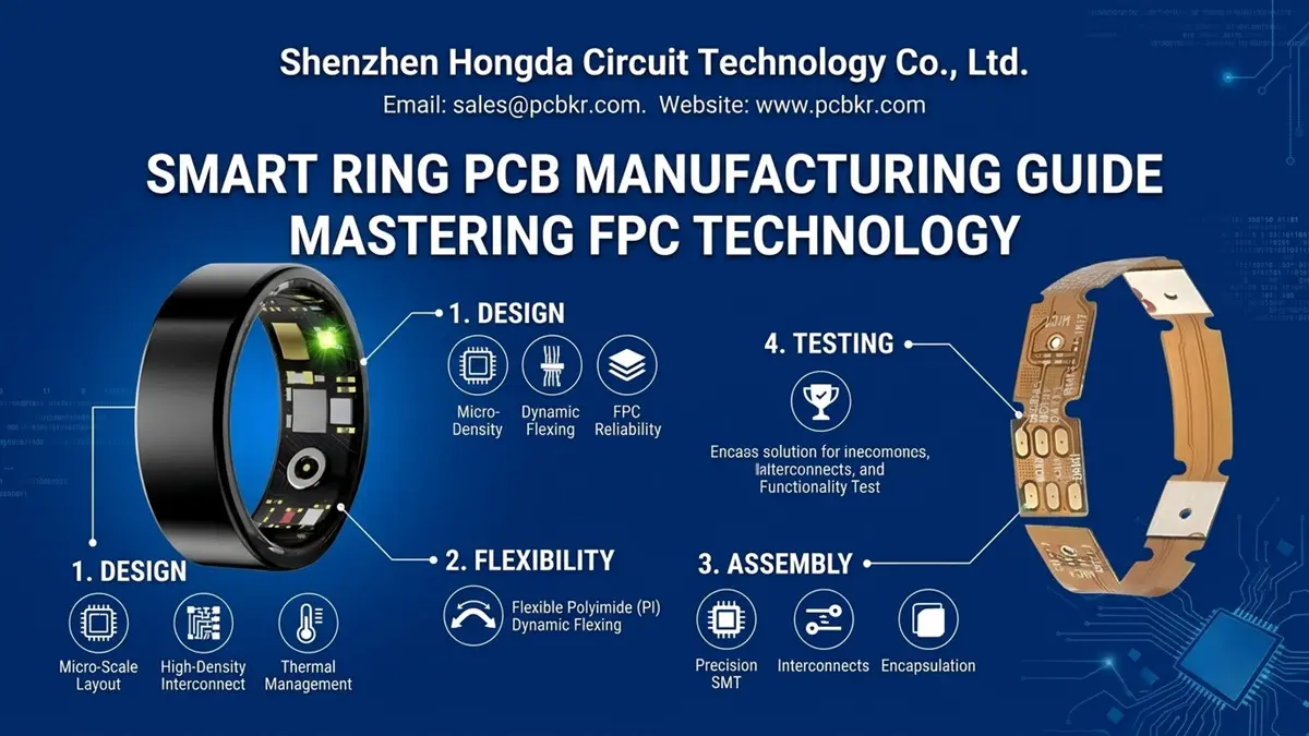
Smart ring PCB manufacturing requires more than reducing a conventional circuit board to a smaller size. OEM projects must balance limited internal space, sensor placement, battery and charging connections, wireless communication, mechanical constraints, assembly yield and long-term reliability. The right PCB architecture depends on the product’s electronics, enclosure and assembly process—not on miniaturization alone.
Shenzhen Hongda Circuit Technology Co., Ltd. manufactures custom PCB solutions under the PCBKR brand, with flexible PCB, rigid-flex PCB and HDI manufacturing capabilities. Our engineering team can review your Gerber files, stack-up, component layout and production requirements to assess manufacturability before tooling and production commitments.
For buyers sourcing a smart ring PCB manufacturer, the practical question is whether the supplier can turn a compact design into a repeatable, inspectable and commercially viable production process.
What PCB Architecture Works Best for a Smart Ring?
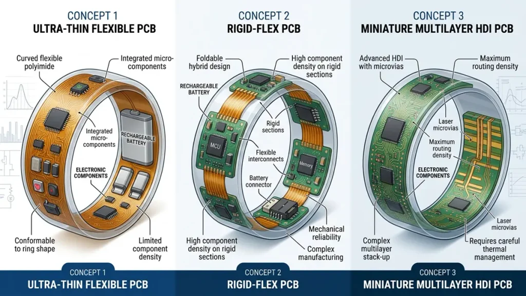
Smart ring PCB architecture options include flexible PCB, rigid-flex PCB, and miniature HDI designs, depending on available space, component layout, and mechanical constraints.
The best smart ring PCB architecture depends on component placement, available volume, required interconnections, mechanical support and target production cost. A flexible PCB may suit a curved or space-constrained layout, while rigid-flex or a compact HDI structure may be appropriate when the design requires denser routing or defined component-mounting regions.
| PCB architecture | When to consider it | Main manufacturing considerations |
|---|---|---|
| Flexible PCB (FPC) | Curved packaging, compact interconnects and limited installation space | Copper type, coverlay openings, bend radius, stiffeners and handling |
| Rigid-flex PCB | A design combining supported component areas with flexible interconnections | Rigid-to-flex transitions, layer registration, lamination and assembly access |
| HDI rigid PCB | Dense component placement and complex routing within a small footprint | Microvia construction, trace spacing, pad design and stack-up |
| Multiple small rigid PCBs with interconnects | Modular electronics or layouts that benefit from separate subassemblies | Connector volume, assembly steps, tolerance stack-up and connection reliability |
A supplier should not recommend rigid-flex automatically simply because the product is a ring. Rigid-flex construction can consolidate interconnections, but it may increase tooling complexity and material cost. A flexible circuit with suitable reinforcement may be more economical for some designs.
For projects requiring curved interconnects or reduced wiring volume, review PCBKR’s Flex PCB manufacturing solutions. For designs that need both supported component regions and flexible connections, see Rigid-Flex PCB manufacturing.
The final construction should be agreed after checking the three-dimensional enclosure, battery position, sensor windows, antenna arrangement, assembly sequence and expected production volume.
Which Advanced PCB Manufacturing Technologies Matter for Smart Rings?
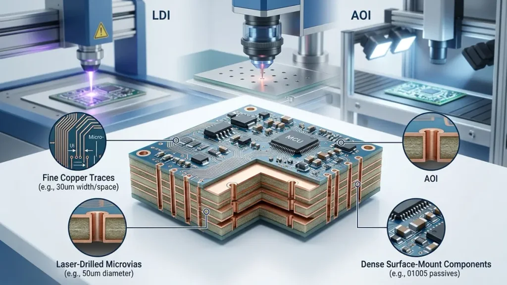
Advanced Smart Ring PCB manufacturing relies on precision imaging, fine-line circuit formation, laser-drilled microvias, and careful multilayer fabrication to support compact wearable electronics
The most useful advanced PCB technologies for smart rings are those that improve routing density, dimensional control and repeatability within a restricted footprint. HDI microvias, laser direct imaging, precision lamination and suitable flexible-circuit materials can help engineers manage these constraints, provided the selected process is appropriate for the actual design.
How does HDI help miniaturize a smart ring PCB?
High-density interconnect technology can create additional routing options where conventional through-hole structures consume too much space. Laser-drilled blind microvias can connect selected layers without requiring every interconnection to pass through the entire board.
PCBKR’s HDI manufacturing capabilities include fine-line fabrication, laser microvia processing and multilayer registration control. Our published HDI PCB capabilities provide further information on the available process options.
For a smart ring project, the relevant engineering questions include:
- Can the required trace width and spacing be manufactured consistently at the proposed panel and production volume?
- Are the microvia diameter, depth, aspect ratio and copper-plating requirements compatible with the selected stack-up?
- Does the design require stacked microvias, staggered microvias or a simpler interconnection structure?
- Are the annular rings, solder-mask openings and component pads suitable for the intended assembly process?
- Can the selected structure be electrically tested and inspected at the required acceptance level?
Smaller features are not automatically better. More aggressive HDI requirements can raise process complexity, inspection demands and cost. The design should use the minimum complexity needed to meet the product’s space and electrical requirements.
How do laser imaging and drilling equipment affect manufacturing precision?
PCBKR’s manufacturing equipment includes SCREEN Ledia laser direct imaging (LDI), Mitsubishi UV/CO₂ laser processing and picosecond laser processing. The suitable process depends on the feature, material, stack-up and production stage.
These equipment capabilities matter in different ways:
- Laser direct imaging: supports accurate circuit-pattern definition and helps manage fine-line fabrication.
- UV/CO₂ laser processing: supports selected drilling and microvia operations according to the applicable process window.
- Picosecond laser processing: provides another option for fine-feature laser work when the material and design justify it.
- Precision lamination: helps control the bonding of layers and the registration of multilayer constructions.
PCBKR’s stated equipment targets include an LDI precision target of 8 µm with ±10 µm tolerance, Mitsubishi UV/CO₂ laser processing around 75 µm ±5 µm, and picosecond laser processing down to 50 µm for applicable features. These are process-specific figures, not a guarantee that every smart ring design can use every minimum feature in stable mass production.
Before quoting, the engineering team should confirm the proposed dimensions against the actual stack-up, materials, copper thickness, via geometry and required production yield. This distinction is particularly important when a design uses ultra-fine features for the first time.
When should a smart ring project use mSAP or ultra-fine circuitry?
Modified semi-additive processing (mSAP) can support finer circuit geometries than conventional subtractive etching in suitable applications. It should be considered when the routing density genuinely requires it, rather than treated as a default specification for all miniature wearables.
PCBKR has stated an 8/8 µm mSAP process target. For a smart ring RFQ, this figure should be treated as an advanced process option subject to engineering review, material compatibility and production-volume validation. Many designs may be manufacturable with less aggressive line-and-space requirements.
The purchasing benefit comes from matching the process to the design: enough routing density to achieve the required footprint, without paying for unnecessarily demanding fabrication specifications.
What Manufacturing Challenges Affect Smart Ring PCB Quality?
Smart ring PCB quality depends on the interaction of circuit geometry, mechanical packaging, assembly, sensor integration and the final enclosure. A bare board can meet its electrical requirements and still cause problems when the assembled electronics are fitted into a compact curved housing.
How should engineers manage flex-zone and rigid-to-flex transition risks?
For flexible circuits, the bend region should be defined before the PCB stack-up is finalized. Copper type, copper thickness, layer arrangement, coverlay, adhesive system and bend radius all influence mechanical performance.
The design review should identify:
- Whether the flex region is static or experiences repeated movement.
- Whether traces cross the bend region and, if so, how they are routed.
- Whether vias, component pads or abrupt geometry changes create local stress concentrations.
- Whether the flex circuit needs stiffeners for component mounting or connector insertion.
- Whether the finished enclosure forces the circuit into a tighter bend than intended.
A flexible PCB’s ability to be bent during assembly does not prove that it will survive repeated bending in service. Dynamic-flex performance must be evaluated using the actual material construction and a defined test method when the application requires it.
How can PPG sensor placement affect PCB and PCBA results?
Some smart rings include photoplethysmography (PPG) sensors, which use optical components to detect changes associated with blood-volume variation. Their performance depends on more than PCB routing.
PCB and assembly suppliers should review the component footprint, sensor orientation, soldering process, nearby components, board geometry and mechanical interfaces. The product team must also consider the optical window, skin contact, enclosure tolerances, ambient-light leakage and firmware signal processing.
A PCB manufacturer can help control board geometry and assembly consistency, but it should not claim that PCB fabrication alone validates heart-rate, oxygen-saturation or other medical performance. Those outcomes require appropriate system-level design and verification.
What can cause smart ring PCB assembly failures?
Common manufacturing risks include solder bridges between closely spaced pads, insufficient solder joints, component misalignment, damaged flex circuits, contamination near optical components and mechanical interference during enclosure assembly.
The risk review should connect each failure mode to a practical control:
| Risk | Recommended review or control |
|---|---|
| Fine-pitch solder bridging | Review pad geometry, solder-mask definition, stencil design and assembly process window |
| Component misalignment | Confirm component pitch, placement access, fiducials and inspection coverage |
| Flex-circuit damage | Define handling points, bend zones, reinforcement and assembly fixtures |
| Optical sensor contamination | Establish cleanliness requirements and protect sensor-facing surfaces |
| Enclosure interference | Check the 3D mechanical model, component heights and tolerance stack-up |
| Intermittent electrical faults | Define electrical test coverage and appropriate acceptance criteria |
For a new design, ask the supplier to identify risks before production rather than waiting for defects to appear during assembly.
How Should Buyers Specify a Smart Ring PCB for Manufacturing?
A useful smart ring PCB specification should describe the required outcome and the constraints that affect production. A single overall board dimension is rarely enough to generate an accurate quotation for a miniature flexible or HDI circuit.
Buyers should prepare the following information where available:
| RFQ item | Information to provide |
|---|---|
| Design files | Gerber or ODB++ files, drill files and fabrication notes |
| Stack-up | Layer count, material type, finished thickness and copper weight |
| Flex construction | Flex-zone drawing, bend conditions, coverlay and stiffener requirements |
| HDI details | Microvia diameter, via structure, trace/space and pad requirements |
| Surface finish | ENIG, OSP or another specified finish, based on assembly and product requirements |
| Assembly scope | BOM, centroid/pick-and-place file, assembly drawing and component sourcing requirements |
| Inspection | Electrical test, AOI, X-ray where applicable, first-article inspection and required reports |
| Production plan | Prototype quantity, forecast volume, order frequency and target schedule |
| Acceptance criteria | Applicable drawings, standards, inspection limits and change-control requirements |
If the design is not finalized, send the current files and mark the open engineering decisions. A supplier can then identify which items are ready for quotation and which need confirmation before the price and schedule can be committed.
For dense routing and microvia requirements, buyers can also review PCBKR’s Microvia PCB manufacturing solutions. This product link supports the technical topic without turning the smart ring article into a duplicate HDI or microvia product page.
How Can Buyers Qualify a Reliable Smart Ring PCB Manufacturer?
A reliable supplier should demonstrate that it can review the design, identify manufacturing risks, document the agreed process and maintain consistent quality as the project moves from prototypes to production. Buyers should compare evidence and scope—not just the unit price.
What manufacturing evidence should a buyer request?
Request evidence that is relevant to the actual board construction and production stage. Depending on the design, this may include:
- A documented DFM review with specific comments on stack-up, clearances, microvias and flex geometry.
- Confirmation of the proposed process limits and any features requiring special approval.
- Representative inspection records, such as AOI results, electrical test records or X-ray inspection where applicable.
- Material and finish specifications, with lot traceability where required.
- A first-article inspection plan and a clear process for approving deviations.
- A written approach to engineering changes, nonconformance handling and repeat orders.
Equipment names alone are not proof of product quality. Ask how the equipment and inspection methods apply to the features in your drawing, and request project-relevant evidence where available.
How should buyers compare prototype and mass-production quotations?
A prototype quote and a mass-production quote may differ because of panel utilization, tooling, material availability, inspection requirements, process yield and order volume. Compare quotes using the same technical scope.
Confirm whether each quotation includes bare PCB fabrication only, component procurement, PCBA assembly, electrical testing, special inspection, packaging and shipping. Also clarify whether the quoted lead time starts after file approval, material confirmation or purchase-order acceptance.
A lower initial price may not be the lowest total cost if the supplier excludes required inspection or cannot support a repeatable production process.
How can PCBKR support smart ring PCB sourcing?
PCBKR’s relevant manufacturing options include flexible PCB, rigid-flex PCB and HDI PCB fabrication, supported by laser imaging, laser processing, lamination and inspection equipment. The exact process route should be selected against the customer’s drawings and acceptance criteria.
For projects requiring both PCB fabrication and assembly, specify the complete scope at RFQ stage. That allows the supplier to evaluate component access, assembly fixtures, inspection needs and the handoff between fabrication and assembly instead of pricing the bare board in isolation.
Request a manufacturing review: Send your Gerber or ODB++ files, stack-up, BOM if assembly is required, expected quantities and target delivery date to PCBKR. The engineering team can review the available information, flag open questions and provide a quotation based on the agreed manufacturing scope.
Email: sales@pcbkr.com Engineering: pcb@pcbkr.com Website: www.pcbkr.com
What Should Be Included in a Smart Ring PCB RFQ?
A smart ring PCB RFQ should contain enough information for the supplier to quote the same construction, quality requirements and delivery scope that the buyer expects to receive. If files or requirements are incomplete, clearly identify the assumptions that the supplier must confirm.
Use this checklist before sending your request:
- Gerber or ODB++ files and drill data.
- Layer stack-up, finished thickness and copper specifications.
- Flex-zone drawing, bend requirements and stiffener details, if applicable.
- Microvia and fine-line specifications, if applicable.
- Surface finish and any material restrictions.
- BOM and assembly files if PCBA is required.
- Prototype quantity and expected production volume.
- Required inspection records, electrical tests and acceptance standards.
- Target schedule, delivery destination and packaging requirements.
- Open design questions or known manufacturing risks.
The more clearly these requirements are defined, the easier it is to compare suppliers on a like-for-like basis and reduce changes after quotation.
Frequently Asked Questions About Smart Ring PCB Manufacturing
How do I choose a reliable smart ring PCB manufacturer?
Choose a manufacturer that can review your actual files, explain the proposed PCB construction, identify manufacturability risks and provide relevant inspection and electrical-test evidence. Confirm that its capabilities match the required flex, HDI, thickness and assembly specifications. Also compare engineering response, change control, lead-time assumptions and repeat-order consistency—not just the quoted price.
Can a PCB manufacturer support smart ring prototypes and mass production?
A supplier may support both stages, but buyers should confirm that the prototype process is suitable for the intended production design. Ask how materials, panelization, inspection, tooling and process controls may change when quantities increase. A successful prototype alone does not establish stable mass-production yield.
Should I choose a flexible PCB or a rigid-flex PCB for a smart ring?
Choose based on the three-dimensional packaging and assembly requirements. Flexible PCB may be suitable for compact interconnections and curved layouts. Rigid-flex may help when the design needs supported component regions integrated with flexible connections. Compare the complete construction, bend conditions, assembly process, interconnection count and total cost before selecting the architecture.
What affects smart ring PCB manufacturing cost and lead time?
The main factors include layer count, board dimensions, material selection, finished thickness, line width and spacing, microvia structure, surface finish, stiffeners, tooling, inspection and order quantity. PCBA adds BOM availability, component sourcing, placement complexity, assembly fixtures and test coverage. An accurate quotation requires the design files and a clearly defined manufacturing scope.
What should I send to a smart ring PCB supplier to get a quotation?
Send Gerber or ODB++ files, drill data, stack-up and fabrication notes. For flexible or rigid-flex designs, include the flex-zone drawing, bend requirements, coverlay and stiffener details. For assembly, include the BOM, centroid file and assembly drawing. Also specify quantities, target lead time, surface finish, inspection requirements and delivery destination.
About Author
David Chen LinkedIn Profile
David Chen is a Senior RF/PCB Process Engineer at Shenzhen Hongda Circuit Technology Co., Ltd., with over 12 years of experience in high-frequency PCB fabrication, impedance-controlled stack-up design, and Rogers/PTFE laminate processing. He also boasts an extensive professional background in PCBA manufacturing, PCBA testing, and PCBA optimization, with specialized expertise in high-precision PCBA fault analysis and rigorous PCBA reliability testing. The author has worked with high-layer-count server PCB fabrication, ultra-low-loss backplane stackups, and thermo-mechanical reliability optimization for AI infrastructure projects involving 112G and 224G PAM4 architectures. Skilled in complex circuit design and cutting-edge advanced PCB manufacturing processes, he delivers solutions that elevate product durability and performance across industrial applications. His technical articles focusing on PCBA manufacturing workflows and testing methodologies are widely cited by industry peers and technical platforms, and have gained attention and recognition from industry colleagues.
, and schematics detailing heavy copper PCB cross-sections, LDI, VCP plating, and laser ablation processes.](https://www.pcbkr.com/wp-content/uploads/2026/07/copper-base-pcb-quote-procurement-guide-hongda-circuit-768x429.webp)