EV Charger PCBA: Smarter Sourcing for Reliable Charging Equipment
EV Charger PCBA quality directly affects the reliability, safety, and production consistency of electric vehicle charging equipment. For OEMs developing AC wallboxes, commercial charging stations, and DC fast chargers, selecting a manufacturing partner requires more than comparing assembly prices. PCB fabrication quality, component sourcing, soldering control, electrical verification, and production traceability all need to match the product’s requirements.
Don’t Choose an EV Charger PCBA Supplier on Price Alone
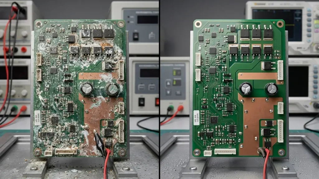
Visual Comparison: Failed Low-Cost vs. Protected Quality EV Charger PCBA
The lowest quotation does not always deliver the lowest total manufacturing cost. An EV charger PCBA project may involve high-current power circuits, low-voltage control electronics, communication interfaces, protection circuits, and components with different thermal requirements.
A quotation that appears competitive may exclude important services such as engineering review, component traceability, X-ray inspection, customized functional testing, or protective coating.
For charging equipment OEMs, the real purchasing objective is to obtain consistent assemblies that meet the approved specifications and can move from prototype to repeat production without avoidable quality problems.
Before comparing quotations, buyers should clarify:
- Whether the project requires bare PCB fabrication, PCBA assembly, or turnkey manufacturing.
- Which components must be sourced from approved manufacturers.
- Which inspection and electrical tests are required.
- Whether conformal coating, potting, or additional mechanical assembly is necessary.
- What production records and traceability information must accompany each delivery.
A meaningful quotation should identify the scope of work, assumptions, exclusions, and testing responsibilities rather than simply provide a price per board.
Common EV Charger PCBA Manufacturing Risks
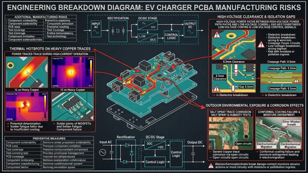
Common EV Charger PCBA Manufacturing Risks and Thermal Breakdown Diagram
EV charging equipment combines electrical, thermal, environmental, and production challenges. The risks differ according to whether the assembly is a control board, metering board, communication board, auxiliary power supply, or high-power conversion board.
High-current circuit performance
Power paths, connector interfaces, copper thickness, and solder joints must be appropriate for the specified current and operating conditions. For high-current designs, OEMs should also evaluate Heavy Copper PCB manufacturing capabilities, including copper thickness control, trace geometry, and thermal management. Inadequate thermal design or poor joint formation can increase resistance and localized heating.
High-voltage insulation requirements
Clearance, creepage, slots, isolation barriers, and component placement must follow the applicable product design and safety requirements. These values cannot be selected from nominal voltage alone; the working conditions, insulation category, materials, and applicable standards also matter.
Mixed component sizes and soldering challenges
An EV charger PCBA may combine fine-pitch surface-mount devices with large inductors, capacitors, power semiconductors, and through-hole connectors. Differences in thermal mass can affect solder-joint formation and process consistency.
Outdoor environmental exposure
Charging equipment installed outdoors may encounter humidity, condensation, dust, and temperature cycling. Depending on the product design, cleaning, conformal coating, potting, connector protection, and material compatibility may need to be addressed.
Component availability and substitutions
Long-lead components and obsolete parts can disrupt production schedules. Unapproved substitutions may also affect electrical performance, thermal behavior, insulation, or product qualification.
These risks should be addressed during engineering review and manufacturing planning, not left until final inspection.
Turn EV Charger PCBA Procurement into a Controlled Process
A controlled sourcing process helps OEMs identify manufacturing problems before they affect delivery schedules or production costs.
1. Define the board’s function
Identify whether the assembly is intended for an AC wallbox, a DC fast charger, a metering module, a control unit, a communication interface, or a power conversion stage. Each application has different electrical and manufacturing priorities.
2. Confirm the manufacturing specifications
Provide the PCB stack-up, copper thickness, board dimensions, material requirements, surface finish, impedance requirements where applicable, and any controlled insulation boundaries.
For assembly, provide the BOM, approved manufacturer part numbers, placement files, assembly drawings, and special process requirements.
3. Complete a design-for-manufacturing review
A DFM review should identify fabrication limitations, component spacing issues, soldering access problems, panelization concerns, and test-access requirements before production begins.
For high-current assemblies, the review should also consider the relationship between copper structures, component pads, terminals, thermal management, and mechanical interfaces.
4. Establish inspection and testing requirements
Inspection should be matched to the assembly’s design and risks. Depending on the project, this may include solder paste inspection, automated optical inspection, X-ray inspection of selected hidden joints, electrical testing, and customer-approved functional tests.
No single inspection method verifies every aspect of board performance. The test plan should specify what each method checks and what evidence is required.
5. Validate the first production build
Prototype and pilot builds provide an opportunity to confirm component availability, manufacturing yield, assembly quality, test coverage, and production documentation.
Any design changes, process adjustments, or approved component substitutions should be documented before the process is released for repeat production.
6. Control repeat manufacturing
Recurring orders require consistent BOM revision control, approved process parameters, inspection criteria, and management of nonconforming products. Serial or lot traceability should be established according to the customer’s product and regulatory requirements.
The Right EV Charger PCBA Manufacturing Partner Reduces Risk
A capable manufacturing partner contributes more than assembly labor. It helps the customer translate design requirements into a repeatable manufacturing process.
For OEM procurement teams, supplier evaluation should focus on verifiable evidence rather than broad claims about quality or advanced technology.
| Evaluation area | Evidence to request |
| PCB fabrication | Stack-up confirmation, material specifications, copper thickness, and relevant inspection records |
| Component sourcing | Approved BOM management, component traceability, and substitution approval procedures |
| SMT and THT assembly | Process capability, inspection plans, and handling requirements for large or sensitive components |
| Quality inspection | Applicable AOI, X-ray, and electrical inspection records |
| Functional verification | An agreed test procedure, acceptance criteria, and records where required |
| Engineering support | DFM feedback, issue resolution, and revision control |
| Production consistency | Pilot-build results, lot identification, and nonconformance management |
For power conversion boards, buyers should also establish who is responsible for high-voltage testing, insulation verification, load testing, thermal validation, and system-level compliance. These responsibilities must be agreed explicitly; general PCBA assembly capability does not automatically establish that every safety or system test is included.
PCBKR Supports EV Charger PCB and PCBA Manufacturing Requirements
Shenzhen Hongda Circuit Technology Co., Ltd. provides PCB fabrication and PCBA assembly services for customers developing electronic products. For EV charger projects, the appropriate manufacturing route depends on the board architecture, electrical requirements, assembly scope, and required verification process.
Relevant manufacturing considerations include:
- PCB fabrication: Stack-up, copper thickness, material selection, fine-line requirements, and dimensional control.
- PCBA assembly: SMT and through-hole assembly according to the approved BOM and assembly documentation.
- Inspection and verification: Available inspection methods include 3D AOI, X-ray inspection, and four-wire Kelvin flying-probe testing, subject to the specific board and test requirements.
- Engineering coordination: Review of manufacturing files, component availability, special process requirements, and production documentation.
- Production planning: Support for prototype, small-batch, and volume-production requirements, subject to project feasibility and confirmed capacity.
For boards containing high-voltage or high-current circuits, OEMs should provide the relevant design constraints and verification requirements early. The proposed manufacturing and test plan can then be reviewed against the actual project scope.
The objective is to establish a documented process that matches the product requirements rather than rely on generic claims of suitability for every EV charger design.
Prepare a Complete EV Charger PCBA RFQ
A complete request for quotation helps the manufacturing team evaluate the project accurately and reduces delays caused by missing information.
Please prepare the following where applicable:
| RFQ information | Recommended files or details |
| PCB fabrication | Gerber or ODB++ files, stack-up, board thickness, copper thickness, surface finish |
| Component procurement | BOM with manufacturer part numbers and approved alternatives |
| Assembly | Pick-and-place files, assembly drawings, polarity details, and special instructions |
| Electrical requirements | Operating voltage, current, insulation requirements, and controlled-impedance specifications where applicable |
| Testing | Required AOI, X-ray, electrical testing, functional test procedures, and acceptance criteria |
| Environmental protection | Cleaning, conformal coating, potting, or other specified requirements |
| Production plan | Prototype quantity, expected recurring volume, target delivery date, and revision status |
| Compliance | Target market, applicable product standards, and customer-specific documentation requirements |
If some information is not yet available, identify the open items so that engineering feasibility can be discussed before the quotation is finalized.
Request an EV Charger PCBA quotation: Send your project requirements and available manufacturing files to sales@pcbkr.com. Include the target quantity, required delivery schedule, and whether you need PCB fabrication, PCBA assembly, or both.
Frequently Asked Questions About EV Charger PCBA
What determines the cost of EV Charger PCBA?
The main factors include PCB layer count, copper thickness, board dimensions, component selection, assembly complexity, testing requirements, protective processes, order quantity, and component availability. A complete RFQ allows these factors to be evaluated together.
Does EV Charger PCBA require heavy copper?
Not every EV charger board requires heavy copper. The appropriate copper thickness depends on current, allowable temperature rise, conductor geometry, thermal conditions, and the design’s electrical requirements. High-current power boards may require heavier copper than control or communication boards.
Which inspections are suitable for EV Charger PCBA?
AOI can identify many visible assembly defects, while X-ray can inspect selected hidden solder joints. Electrical and functional testing can verify additional characteristics when appropriate test methods and acceptance criteria are defined. The required combination depends on the board design and product risks.
Can one supplier manufacture the PCB and assemble the components?
Yes, a supplier offering both PCB fabrication and PCBA assembly can coordinate these stages under one project scope. Buyers should confirm component sourcing, testing, documentation, and any outsourced processes before placing an order.
What should OEMs provide when requesting an EV Charger PCBA quotation?
Provide the PCB manufacturing files, BOM, assembly files, technical specifications, required tests, target quantities, and delivery schedule. Clearly identify applicable safety requirements and special processes so that the supplier can assess feasibility and define the quotation scope.
Conclusion
EV Charger PCBA procurement should be treated as a manufacturing-risk management decision rather than a price comparison exercise. Clear specifications, early engineering review, appropriate inspection, controlled component sourcing, and documented verification help OEMs improve production consistency and reduce avoidable delays.
For EV charger developers seeking PCB fabrication or PCBA assembly support, the next step is to provide the actual board files and project requirements for a manufacturing feasibility review and quotation.
About Author
David Chen LinkedIn Profile
David Chen is a Senior RF/PCB Process Engineer at Shenzhen Hongda Circuit Technology Co., Ltd., with over 12 years of experience in high-frequency PCB fabrication, impedance-controlled stack-up design, and Rogers/PTFE laminate processing. He also boasts an extensive professional background in PCBA manufacturing, PCBA testing, and PCBA optimization, with specialized expertise in high-precision PCBA fault analysis and rigorous PCBA reliability testing. The author has worked with high-layer-count server PCB fabrication, ultra-low-loss backplane stackups, and thermo-mechanical reliability optimization for AI infrastructure projects involving 112G and 224G PAM4 architectures. Skilled in complex circuit design and cutting-edge advanced PCB manufacturing processes, he delivers solutions that elevate product durability and performance across industrial applications. His technical articles focusing on PCBA manufacturing workflows and testing methodologies are widely cited by industry peers and technical platforms, and have gained attention and recognition from industry colleagues.