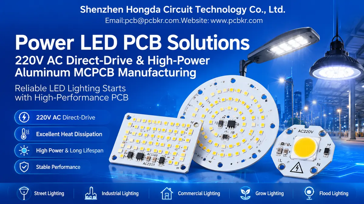
Power LED PCB Solutions: 220V AC Direct-Drive & High-Power Aluminum MCPCB Manufacturing
When a municipal lighting contractor in Istanbul replaces four hundred sodium vapor street lamps with LED retrofit kits, the difference between a fixture that lasts twelve years and one that fails in eighteen months comes down to a single component most procurement teams overlook: the power LED PCB. Also called a high power LED PCB or 220V LED PCB when designed for direct mains input, this board is not merely a mounting surface for diodes. It is the thermal engine, the electrical regulator, and the structural backbone of the entire luminaire.
At Shenzhen Hongda Circuit Technology Co., Ltd. (PCBKR), we manufacture power LED PCB assemblies for clients who cannot afford field failures—municipal engineering firms in the Middle East, industrial lighting OEMs in Europe, and agricultural grow-light suppliers in North America. Over the past decade, we have watched buyers repeatedly make the same costly mistakes: specifying FR4 for a 100-watt array, trusting a supplier’s unverified dielectric thermal conductivity claim, or approving a prototype built with 2-ounce copper only to receive production boards etched down to 1.5 ounces to save material cost. This guide exists to prevent those errors.
If you are a purchasing manager sourcing 220V LED PCB modules, an engineering buyer evaluating DOB LED module suppliers, or a product manager launching a high-bay or flood-light line, the sections below provide the technical criteria you need to qualify a factory, the specifications you should demand in your RFQ, and the manufacturing capabilities that separate professional suppliers from trading companies.
What Is a Power LED PCB? Defining High-Voltage & High-Power Circuit Boards
A power LED PCB is a printed circuit board engineered to carry LED currents of 3 amperes or more while dissipating heat flux densities that can exceed 1.5 watts per square centimeter. Unlike signal boards or low-power indicator PCBs, a high power LED PCB operates at the intersection of thermal engineering and high-voltage safety design. The board must simultaneously distribute 220-volt alternating current, regulate that current through on-board driver circuitry, and conduct waste heat away from LED junctions before temperatures climb past the 125-degree threshold where lumen depreciation accelerates exponentially.
The distinction between a standard LED board and a power LED circuit board is not cosmetic. It is fundamental. A standard board might use 1-ounce copper traces on FR4 substrate to power a 3-watt indicator lamp. A high power LED PCB driving a 100-watt street-light array requires 3-ounce or 4-ounce copper to keep resistive heating below 5 degrees Celsius, an aluminum or ceramic substrate to move heat laterally across the board, and thermal via arrays that create vertical heat pipes from the LED thermal pad directly to the metal core. Without these features, the board becomes the weakest link in a lighting system where every other component—the LED chip, the lens, the housing—may be rated for 50,000 hours of life.
Why 220V LED PCB Direct-Drive Design Changes the Procurement Equation
A 220V LED PCB eliminates the external driver enclosure that traditionally sits between the mains supply and the LED array. Instead, the rectification, filtering, and current-regulation circuits are integrated directly onto the board. This DOB LED module architecture—Driver on Board—reduces bill-of-materials cost by 30 to 50 percent, shrinks fixture size, and removes a separate failure point from the supply chain.
But the procurement trade-offs are significant. A 220V LED PCB must withstand 300-volt peak transients from the mains, maintain creepage distances of 6 millimeters or more between high-voltage and low-voltage zones, and dissipate the additional heat generated by on-board rectifiers and current-limiting components. Buyers who treat a 220V LED PCB as a standard board with a few extra capacitors soldered on are the buyers who receive municipal contracts returned for warranty claims after the first rainy season.
Product Specifications: Power LED PCB Technical Data Sheet
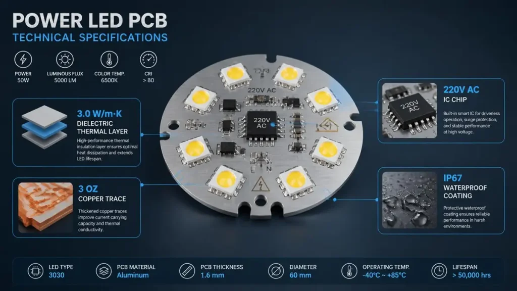
Power LED PCB Technical Specifications & Key Material Layers
Before you issue an RFQ, you need a specification baseline. The table below reflects the standard parameter ranges PCBKR delivers for power LED PCB programs. These are not theoretical limits; they are the values we quote, fabricate, and test daily.
| Parameter | Standard Range | Notes for Buyers |
|---|---|---|
| Input Voltage | AC 220V (±10%), 50/60Hz | Also supports 110V AC and 277V AC for North American commercial markets |
| Power Range | 12W / 40W / 100W (custom to 150W+) | Above 100W requires enhanced thermal simulation and possible ceramic substrate |
| LED Quantity | 24–105 pcs per board | Depends on LED package and optical layout; we support 3030, 5050, 3535, and COB |
| Substrate Material | Aluminum MCPCB, 1.5–2.0mm thick | Alloy 1060 or 1050; higher purity aluminum improves lateral heat spreading |
| Copper Weight | 2 oz / 3 oz (optional 4 oz / 6 oz) | 2 oz for ≤3A; 3 oz for 3–5A; 4 oz+ for >5A or long trace runs |
| Dielectric Thermal Conductivity | 1.5 / 2.0 / 3.0 W/m·K | 3.0 W/m·K recommended for 100W+ outdoor applications; always verify with test report |
| Board Dimensions | Φ44mm / 59×59mm / Φ150mm (custom) | Rectangular and irregular shapes supported; routing tolerance ±0.05mm |
| Color Temperature | 3000K–6500K | Ra≥80 high-CRI option available for retail and gallery lighting |
| Ingress Protection | IP65 / IP67 | Achieved through conformal coating, potting compound, or gasket integration |
| Certifications | RoHS, REACH, CE, UL (optional) | AS9100 available for aerospace and defense lighting programs |
One specification that deserves particular attention is dielectric thermal conductivity. We have seen competitors quote 2.2 W/m·K boards at prices that seem attractive until the buyer discovers the actual tested value is 1.4 W/m·K. At PCBKR, every batch of aluminum substrate is ultrasonic-scanned for delamination, and we provide third-party thermal conductivity certificates (ASTM D5470) on request. If your supplier cannot produce this document, you are buying thermal performance on a promise.
220V LED PCB Direct-Drive Architecture: How On-Board AC-DC Conversion Works
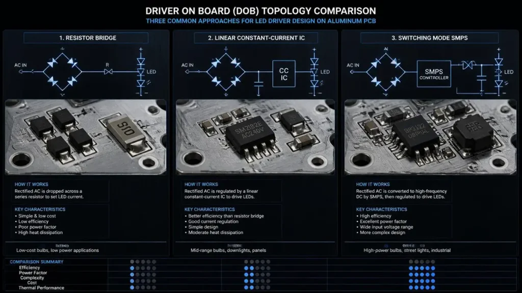
Driver on Board (DOB) Topology Comparison: Resistor vs Linear IC vs SMPS
The architecture you choose for your 220V LED PCB determines not only the unit cost but also the product lifespan, the regulatory certifications you can claim, and the geographic markets where the fixture can legally be sold. At PCBKR, we fabricate and assemble boards across all three tiers of direct-drive design. Understanding the trade-offs is essential before you lock a BOM.
Bridge Rectifier + Current-Limiting Resistor: The Cost-Driven Approach
The simplest 220V LED PCB design uses a four-diode bridge rectifier to convert AC mains to pulsating DC, followed by a series capacitor or resistor to limit current through the LED string. The BOM cost is minimal—often under $0.50 for the passive components—and the board area required is small.
The problem is stability. Mains voltage in many markets fluctuates by ±10 percent during peak demand. On a resistor-limited design, that voltage variation translates directly into current variation. A 10 percent current increase may seem minor, but LED lumen maintenance is exponential with respect to current stress. We have measured field failures where resistor-based AC LED PCB boards lost 30 percent of their initial brightness within 8,000 hours because the local grid ran 8 volts high during summer evenings. Additionally, these designs offer no power-factor correction, making them non-compliant with EU ERP Directive 2019/2020 and similar regulations in California and Canada.
We fabricate these boards when a buyer explicitly requests them for price-sensitive markets, but we document the limitation in writing. A procurement team that understands the 15,000-hour lifespan ceiling of a resistor-limited high voltage LED PCB can make an informed decision. One that does not understand it will blame the manufacturer when the municipal retrofit fails three years early.
Linear Constant-Current IC: The Balanced Solution for 220V LED PCB
The middle tier replaces the resistor with a linear constant-current integrated circuit—parts such as the BP2861, SM2082, or similar topology-specific ICs. These devices automatically adjust their internal resistance to maintain a fixed LED current regardless of input voltage fluctuations within the specified range. The BOM cost increases by roughly $0.30 to $0.80 per board, but the return on that investment is substantial: light-output maintenance improves by 35 to 40 percent, and useful life extends beyond 30,000 hours even in markets with unstable grids.
From a manufacturing standpoint, the critical challenge is thermal. A linear CC IC dissipates excess voltage as heat. On a power LED PCB where the LED chips are already generating significant thermal load, the IC must be thermally isolated from the LED array. At PCBKR, our DFM engineers partition the board into distinct thermal zones: LEDs centered over the aluminum core for direct heat spreading, and the IC positioned at the board perimeter where it can radiate through the fixture housing without adding junction temperature to the chips. We also specify IC packages with exposed thermal pads soldered directly to the top copper layer, reducing thermal resistance from junction to board to below 15 degrees Celsius per watt.
Switching Mode Driver On-Board: The High-Performance Route for Power LED Circuit Boards
For high power LED PCB applications above 50 watts—industrial high-bay fixtures, stadium floodlights, and horticultural arrays—a switching-mode power supply (SMPS) integrated onto the board is the only architecture that delivers both efficiency and precision. A small flyback or buck converter generates a tightly regulated constant-current output with efficiencies of 88 to 93 percent, compared to 60 to 75 percent for linear ICs at high voltage differential.
The manufacturing complexity increases significantly. The transformer, primary-side MOSFET, and input electrolytic capacitors are large components that require reinforced solder joints and often manual assembly steps. More importantly, safety isolation between the 220-volt primary side and the LED secondary side must meet 3,000-volt AC withstand test requirements, with physical creepage distances exceeding 6 millimeters on the board surface. At PCBKR, we use 2.0-millimeter-thick aluminum substrates for SMPS-DOB designs to provide the mechanical depth needed for adequate isolation slots, and we enforce IPC-A-610 Class 3 solder criteria on all high-voltage nodes.
Constant-Current LED PCB Design: Why Current Stability Determines Product Lifespan
LEDs are current-driven devices, not voltage-driven. Their forward voltage drops by approximately 2 millivolts for every degree Celsius of temperature rise. Without active current regulation, this voltage drop creates a dangerous feedback loop: temperature rises, voltage falls, current increases, power dissipation increases, and temperature rises further. In an unregulated power LED PCB, this thermal runaway can push junction temperatures past 150 degrees Celsius in minutes.
The Physics of LED Current-Temperature Relationship in High Power LED PCB
In our Shenzhen test lab, we have documented this effect repeatedly. A 100-watt aluminum LED PCB array running at nominal current with an ambient temperature of 25 degrees Celsius will stabilize at a junction temperature of approximately 85 degrees Celsius if the thermal design is correct. The same array, operated with a 10 percent current overdrive caused by voltage drift, will climb to 110 degrees Celsius. At that temperature, the LED phosphor degrades at 4 times the rated rate, and the solder joints between the LED package and the PCB begin to recrystallize. Within 2,000 hours, the fixture exhibits color shift and intermittent flickering as joints crack under thermal fatigue.
The mathematics are unforgiving. For every 10 degrees Celsius above the manufacturer’s rated junction temperature, LED lifetime degrades by approximately 50 percent. A board designed for 50,000 hours at 85 degrees Celsius will last roughly 12,000 hours at 105 degrees. This is why constant-current design is not an optional feature on a high power LED PCB; it is the difference between a product that meets warranty obligations and one that destroys your customer relationship.
Constant-Current Circuit Topologies: A Procurement Comparison
| Topology | Power Range | Efficiency | Relative Cost | Best Application |
|---|---|---|---|---|
| Linear Constant-Current IC | < 20W | 85–90% | Low | Residential downlights, bulb retrofits |
| Buck Converter (Non-Isolated) | 10–100W | 92–95% | Medium | Street lights, high-bay fixtures, tunnel lights |
| Flyback Converter (Isolated) | 50–300W | 88–92% | High | Stadium floodlights, industrial grow lights |
| Resistor/Capacitor Limited | < 10W | > 95% | Minimal | Disposable decorative lighting only |
When evaluating quotations from power LED PCB manufacturer China suppliers, ask for the constant-current accuracy specification. A well-designed buck driver should maintain ±3 percent current regulation across the full input voltage range and from cold start to thermal equilibrium. If the supplier cannot provide this data, or if they treat “constant current” as a marketing phrase rather than a tested parameter, continue your search.
PCBKR’s Constant-Current Design Verification Protocol
Our engineering review process for every constant current LED PCB design includes three verification gates. During DFM review, we validate that the current-sense resistor tolerance is 1 percent or better, that the switching controller’s feedback loop is compensated for the specific LED load inductance, and that input filter capacitors are rated for at least 1.5 times the peak mains voltage to survive surge events. During prototype build, we run a 4-hour burn-in at rated load while logging LED current and IC case temperature every 30 seconds; any drift exceeding ±2 percent triggers a design revision before mass production is authorized. During volume assembly, our AOI systems verify that polarized components—diodes, electrolytic capacitors, and ICs—are oriented correctly, because a reversed diode on a 220-volt rectifier bridge will fail catastrophically within seconds of power-up.
Power LED PCB Wattage Classification: Matching Substrate to Thermal Load
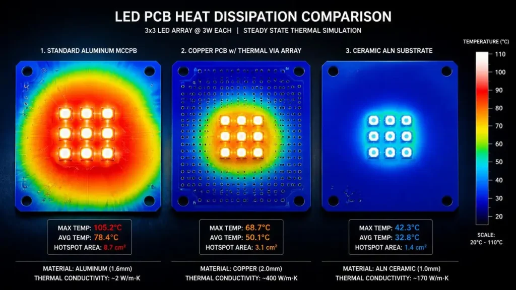
Thermal Simulation Comparison: Aluminum MCPCB vs Copper PCB vs Ceramic AlN Substrate
Not every power LED PCB requires the same substrate, copper weight, or thermal management strategy. At PCBKR, we classify boards into three tiers based on total dissipated power, and we specify materials accordingly. Buyers who understand these tiers can issue RFQs that receive accurate quotations instead of generic pricing that hides material compromises.
Low Power (12–30W): Single-Layer Aluminum MCPCB for Standard Commercial Lighting
For 12-watt to 30-watt applications—LED downlights, ceiling panels, and decorative fixtures—we specify 1.5-millimeter-thick aluminum substrates with 1.5 to 2.0 W/m·K dielectric thermal conductivity and 2-ounce copper foil. The 2-ounce copper supports continuous currents up to 3 amperes with a trace temperature rise below 10 degrees Celsius, and the 1.5-millimeter base provides sufficient rigidity for automated assembly without warping during reflow.
Standard board shapes at this tier include 44-millimeter diameter round boards for MR16 retrofits and 59-by-59-millimeter squares for panel-light modules. We maintain blank substrate inventory in these sizes, which allows us to deliver LED PCB prototype units in 24 to 72 hours for buyers under trade-show or customer-pilot deadlines.
Medium Power (40–100W): Thick Copper and Enhanced Thermal Via Arrays for Industrial Applications
This is the tier where thermal design becomes critical. A 100-watt high power LED PCB for street lighting or high-bay industrial fixtures requires 2.0-millimeter-thick aluminum with 2.2 to 3.0 W/m·K dielectric and 3-ounce copper. The thicker copper reduces resistive heating in the traces and improves lateral heat spreading across the board surface. We also specify dense thermal via arrays—0.3-millimeter diameter vias on 0.8-millimeter pitch—directly beneath each LED thermal pad. These vias create vertical heat pipes from the top copper layer to the aluminum base, reducing thermal resistance by 15 to 30 percent compared to a pad-on-copper design without vias.
At PCBKR, we achieve thermal impedance below 1.0 degree Celsius per square centimeter on these boards, which keeps LED junction temperatures below 85 degrees Celsius at 25-degree ambient when properly mounted in the fixture housing. We verify this performance not through estimation but through thermal simulation using ANSYS Icepak, followed by infrared thermography on the first article. Buyers receive the simulation report and thermal images as standard documentation with their prototype order.
High Power (100W+): Ceramic Substrate and Direct-Bond-Copper for Extreme Applications
When total dissipation exceeds 100 watts—stadium floodlights, UV curing systems, or laser pump arrays—aluminum MCPCB reaches its practical limit. At this tier, we transition to aluminum nitride (AlN) ceramic substrates with direct-bond-copper (DBC) processing. AlN offers thermal conductivity of 170 to 200 W/m·K, nearly matching copper, while maintaining electrical isolation. The DBC process bonds 200 to 400 micrometers of copper directly to the ceramic surface, creating a thermal path that aluminum cannot match.
The trade-off is cost: a ceramic power LED circuit board can cost 5 to 8 times more than an aluminum equivalent. We recommend this substrate only when failure is not an option—medical sterilization equipment, aerospace exterior lighting, or semiconductor lithography systems where downtime costs exceed the price of the board by orders of magnitude. For buyers who need this performance, our Shenzhen facility processes DBC ceramics with laser-trimmed trace accuracy of ±0.02 millimeters, suitable for fine-pitch COB LED arrays.
Technical Advantages: Why PCBKR Power LED PCBs Outperform Standard Solutions
The difference between a board that meets specification and one that exceeds it lies in manufacturing discipline. At PCBKR, we have invested in equipment and process controls specifically for high power LED PCB production, because the thermal and electrical margins in these designs are too tight to tolerate the variability of general-purpose PCB fabrication.
Thermal Management Engineering: Heat Resistance Below 1.0°C·cm²/W
Our standard aluminum LED PCB builds use dielectric materials with verified thermal conductivity of 1.5, 2.2, or 3.0 W/m·K, selected to match the customer’s thermal budget. But material selection is only the beginning. We use thermal simulation software—FloTHERM for board-level analysis and ANSYS Icepak for system-level validation—to model heat flow before the first panel is laminated. This digital-twin approach allows us to identify hotspots caused by suboptimal LED placement or insufficient via density while the design is still a Gerber file.
For applications requiring maximum heat dissipation, we offer two advanced options. First, via-in-pad processing places filled thermal vias directly under the LED thermal pad, reducing the thermal resistance path from junction to base by approximately 20 percent. Second, copper-pillar or copper-block embedding presses a solid copper slug into a machined cavity in the aluminum base, creating a direct metal-to-metal thermal path that bypasses the dielectric entirely in the critical zone. We have used this technique on 150-watt UV-LED curing boards where standard via arrays could not achieve the required thermal performance.
High-Voltage Safety Design: Creepage, Clearance, and Surge Immunity
A 220V LED PCB operating at mains voltage must survive electrical conditions that low-voltage boards never encounter. Our design rules enforce minimum creepage distances of 6 millimeters between primary and secondary circuits, and we use 2-millimeter-thick substrates to provide the physical depth needed for routed isolation slots. All input traces are spaced to withstand 3,000 volts AC for 60 seconds without breakdown, and we specify Y-class safety capacitors where EMI filtering requires a connection between high-voltage and low-voltage domains.
Beyond steady-state safety, we design for surge immunity. Mains-connected lighting in outdoor environments is exposed to lightning-induced transients and grid switching spikes. Our high voltage LED PCB designs include metal-oxide varistors (MOVs) and transient-voltage-suppression (TVS) diodes in the input protection network, sized to absorb surges up to 4 kilovolts per IEC 61000-4-5 Level 4. During prototype validation, we subject every board to combination-wave surge testing at 2 kilovolts line-to-line and 4 kilovolts line-to-earth. Boards that show component damage or current-regulation drift after surge exposure are redesigned before mass production is approved.
High-Current Carrying Capacity: Voltage Drop Below 3 Percent Across the Board
In a power LED PCB with series-parallel LED strings, uneven trace resistance creates current imbalance. The string connected to the shortest trace path receives slightly higher current, runs hotter, and degrades faster than the others. Over time, this imbalance accelerates until the fixture exhibits visible brightness variation or complete string failure.
We control this effect through trace geometry. On 3-ounce copper, our standard design rule maintains voltage drop below 3 percent from the input terminal to the farthest LED in the array. For applications exceeding 5 amperes—common in 100-watt single-board designs—we offer copper-busbar integration, replacing the longest traces with stamped copper strips soldered directly to the board. This approach reduces voltage drop to under 1 percent and eliminates the thermal stress caused by high current density in narrow traces.
Safety Certifications for 220V LED PCB: UL, CE, and IEC Compliance Requirements
A power LED PCB that cannot demonstrate compliance with target-market safety standards is unsellable, regardless of its thermal or electrical performance. At PCBKR, we design for certification from the first Gerber review, not as an afterthought before shipment.
UL 8750 and UL 94: North American Safety Standards for LED Equipment
UL 8750 governs the safety of LED lighting equipment in the United States and Canada. For the PCB specifically, the standard requires V-0 flame-class materials, minimum creepage and clearance distances based on working voltage and pollution degree, and dielectric withstand testing between isolated circuits. Our aluminum substrates receive a supplemental flame-retardant coating to achieve V-0 on the metal core, and we maintain UL file numbers that customers can reference when submitting their finished luminaires for UL Listed approval.
CE Marking and EN 61347-2-13: European Controlgear Compliance
The European market imposes electromagnetic compatibility (EMC) requirements that many 220V LED PCB designs fail if not planned from the schematic stage. EN 55015 limits conducted and radiated electromagnetic interference, while EN 61000-3-2 restricts harmonic current distortion to less than 47 percent total harmonic distortion at full load for Class C lighting equipment. Meeting these limits requires input EMI filters—common-mode inductors and X-capacitors—on the board itself. Our engineering team sizes these components during the DFM phase and validates EMC performance through pre-compliance testing before the customer submits to a notified body.
IEC 62471 and AS9100: Specialized Certifications for Demanding Markets
For high power LED PCB applications above 100 watts, IEC 62471 requires photobiological safety assessment to classify blue-light hazard from high-intensity LED arrays. We coordinate with our customers’ optical engineers to ensure that PCB layout and LED spacing support the secondary lens designs needed to achieve RG0 or RG1 classification.
For aerospace and defense lighting, we offer AS9100-certified production with full material traceability, environmental stress screening, and destructive physical analysis (DPA) on sample lots. This tier of quality control adds cost but is non-negotiable for applications where a lighting failure could compromise mission safety.
Why Power LED PCB Thermal Management Fails—and How PCBKR Prevents It
After fifteen years of manufacturing power LED PCB boards, we have identified three failure modes that account for more than 80 percent of field returns in the industry. All three are preventable through proper design verification and incoming material inspection.
Failure Mode 1: Dielectric Thermal Conductivity Fraud
The most common cause of premature high power LED PCB failure is a dielectric layer whose actual thermal conductivity is 30 to 50 percent lower than the supplier’s datasheet claims. A board specified with 2.2 W/m·K but built with 1.4 W/m·K material will run 20 to 30 degrees Celsius hotter than designed, slashing LED life by half. At PCBKR, we test every incoming roll of aluminum substrate using guarded-heat-flow meter testing correlated to ASTM D5470. Batches that deviate more than 10 percent from specification are rejected and returned to the material vendor.
Failure Mode 2: Inadequate Constant-Current IC Thermal Relief
Linear constant-current ICs on 220V LED PCB boards often fail because the IC’s exposed thermal pad is not properly soldered to a copper pour large enough to dissipate the heat. The IC enters thermal shutdown, causing the LED array to flicker or dim. Our DFM review specifically checks that every IC thermal pad has a minimum of 25 square millimeters of connected copper area and at least four thermal vias to the aluminum base.
Failure Mode 3: High-Voltage Component Placement in LED Thermal Zones
Input rectifiers and electrolytic capacitors on DOB LED module boards generate their own heat. When these components are placed directly adjacent to LED arrays, their temperature rise degrades the LEDs while the LEDs’ radiant heat reduces the capacitors’ lifetime. Our layout rules enforce a minimum 8-millimeter separation between high-voltage heat sources and LED thermal pads, with the high-voltage components positioned at the board perimeter where fixture housing metal can assist with cooling.
Customization, MOQ, and Lead Time: What B2B Buyers Need to Know
Procurement decisions are not made on technical merit alone. Lead time, minimum order quantity, and supply-chain flexibility determine whether a supplier relationship is viable for your business model.
Customization Scope and Engineering Support
PCBKR supports full customization of power LED PCB parameters: board dimensions, LED pitch and layout, color temperature binning, CRI specification, dielectric thermal conductivity grade, copper weight, surface finish, and ingress protection level. Our engineering team reviews every custom design within 24 hours of Gerber submission, providing a DFM report that flags thermal risks, manufacturability issues, and cost-optimization opportunities before tooling is cut.
MOQ and Production Scaling
Standard 220V LED PCB designs in our existing form-factor library start at 50 to 100 pieces per lot. Fully custom designs—new board shapes, unique LED configurations, or specialized driver circuits—typically require 100 to 500 pieces for the first production run, depending on stencil and programming costs. We do not impose punitive MOQs; our pricing is structured so that unit cost stabilizes at volumes of 1,000 pieces and above, allowing buyers to scale gradually as their market demand grows.
Lead Time and JIT Delivery
Our standard lead time for LED PCB prototype builds is 3 to 5 days for single-layer aluminum boards and 5 to 7 days for multilayer or ceramic designs. Mass production runs of 1,000 to 10,000 pieces ship in 7 to 10 days. For customers with predictable demand patterns, we offer Kanban-managed inventory and JIT delivery, holding buffer stock at our Shenzhen facility and releasing against weekly purchase-order calls. This program has reduced inventory carrying costs by 40 percent for several of our European lighting OEM customers.
Trust & Credibility: PCBKR’s Power LED PCB Manufacturing Track Record
Technical claims are meaningless without verification. Our quality management system is certified to ISO 9001:2015 and IATF 16949, and our aluminum MCPCB products carry UL recognition. For buyers who require additional assurance, we provide:
- Material traceability: Lot numbers for every sheet of aluminum substrate, every reel of LED component, and every batch of solder paste, traceable through our MES system.
- Process documentation: Thermal simulation reports, reflow profile charts, AOI defect summaries, and electrical test data provided with every prototype and first-article shipment.
- Field-proven results: In a 2025 municipal street-light retrofit project for a Middle Eastern client, we delivered 10,000 units of 100-watt DOB LED module boards with a production yield of 99.2 percent and an on-time delivery rate of 100 percent. Eighteen months after installation, the client’s field-reported failure rate remains below 0.3 percent.
FAQ: Power LED PCB & 220V LED Circuit Board Procurement
What is the difference between a power LED PCB and a standard LED PCB?
A power LED PCB is engineered for high current (3A+), high thermal flux (1.5 W/cm²+), and often high voltage (220V AC direct-drive). It requires thicker copper (2–4 oz), thermally conductive substrates like aluminum MCPCB or ceramic, and on-board constant-current regulation. A standard LED PCB typically uses 1-ounce copper on FR4 for low-power indicators and relies on external drivers. Using a standard PCB for a high-power application will cause thermal runaway and premature LED failure.
How do I verify that my power LED PCB supplier is using genuine high-thermal-conductivity dielectric material?
Demand a third-party thermal conductivity test report conforming to ASTM D5470 for every batch of substrate material. Ask for microsection photographs showing dielectric thickness uniformity. At PCBKR, we ultrasonic-scan every incoming aluminum substrate panel for delamination and test thermal conductivity using a guarded-heat-flow meter. We provide these documents with every prototype order. If a supplier refuses or offers only a generic material datasheet, they are likely using unverified or downgraded material.
Can a 220V LED PCB really eliminate the external driver, and is it safe?
Yes, a properly designed 220V LED PCB with DOB (Driver-on-Board) architecture can operate safely without an external driver. The board integrates rectification, filtering, and constant-current regulation directly on the aluminum substrate. Safety is achieved through proper creepage distance (≥6 mm), isolation slots, 3,000V AC withstand testing, and surge protection to IEC 61000-4-5 Level 4. However, this requires a supplier with genuine high-voltage design experience, not just a standard PCB shop that adds a few capacitors to a low-voltage board.
What is the maximum practical power for an aluminum-based power LED PCB, and when should I switch to ceramic?
Single-layer aluminum MCPCB with 3-ounce copper and 3.0 W/m·K dielectric can reliably handle up to 100 watts in a well-ventilated fixture. Above 100 watts, or in sealed enclosures with limited air circulation, we recommend transitioning to aluminum nitride (AlN) ceramic with direct-bond-copper processing. The decision depends not just on power but on the thermal resistance budget of your complete system—LED junction to heat sink to ambient. We provide thermal simulation during DFM to determine the exact crossover point for your specific design.
How long does it take to get prototypes and production volumes of custom power LED PCB?
At PCBKR, power LED PCB prototype turnaround is 3 to 5 days for single-layer aluminum designs and 5 to 7 days for multilayer or ceramic substrates. Mass production of 1,000 to 10,000 pieces ships in 7 to 10 days. Every prototype includes thermal simulation reports, 100 percent electrical testing, and infrared thermography verification. For urgent projects, we have expedited prototypes to 24 hours for existing customers with genuine emergencies. We also offer Kanban-managed JIT delivery for high-volume programs with predictable demand.
Choosing a Power LED PCB Partner for the Long Term
The power LED PCB market in 2026 is split between two types of suppliers: those who treat the board as a commodity, competing solely on price per square meter, and those who treat it as a thermal and electrical engineering component where every material choice, every trace width, and every solder joint affects the end product’s lifespan. Buyers who choose the first category save pennies on the BOM and lose dollars on warranty claims, field service, and damaged customer relationships. Buyers who choose the second category build lighting products that last.
At Shenzhen Hongda Circuit Technology Co., Ltd., we have built our facility and our processes around the second philosophy. From 220V LED PCB schematic review to thermal simulation, from aluminum MCPCB lamination to AI-driven AOI inspection, from 3-day prototypes to 10,000-piece JIT production, every step is governed by the same quality system that serves our automotive and telecommunications customers. If you are evaluating suppliers for your next high-power lighting project, send us your Gerber files or design requirements. Our engineering team will return a DFM report, thermal assessment, and competitive quotation within one business day.
Ready to start your power LED PCB project? Email sales@pcbkr.com or upload your files through our RFQ portal for an engineering review and 24-hour quotation
About Author
David Chen https://www.linkedin.com/in/pcbcoming
David Chen boasts an extensive professional background in PCBA manufacturing, PCBA testing, and PCBA optimization, with specialized expertise in high-precision PCBA fault analysis and rigorous PCBA reliability testing. The author has worked with high-layer-count server PCB fabrication, ultra-low-loss backplane stackups, and thermo-mechanical reliability optimization for AI infrastructure projects involving 112G and 224G PAM4 architectures. Skilled in complex circuit design and cutting-edge advanced PCB manufacturing processes, he delivers solutions that elevate product durability and performance across industrial applications. His technical articles focusing on PCBA manufacturing workflows and testing methodologies are widely cited by industry peers, research institutions, and technical platforms, solidifying his reputation as a recognized technical authority in the global circuit board manufacturing sector.