How Do You Choose a Solar Inverter PCBA Manufacturer for OEM Production?
A reliable solar inverter PCBA manufacturer should be able to build the required control, power, MPPT, and protection boards to the OEM’s released design, while controlling PCB fabrication, component assembly, inspection, and agreed electrical tests. The right supplier must also review high-voltage spacing, current paths, thermal constraints, and production requirements before quotation.
Solar Inverter PCBA Product Details
Shenzhen Hongda Circuit Technology Co., Ltd. provides PCB fabrication and PCBA assembly services for OEM electronic products. For solar inverter projects, the manufacturing scope can be evaluated according to the actual board architecture, component package, PCB construction, assembly process, and test requirements supplied by the customer.
Solar inverter PCBA project types may include:
- Solar Inverter Control Board: Control and monitoring circuits for inverter operation, sensing, communication, and protection.
- Solar Inverter Power Board: PCB assemblies used in power conversion and switching sections, subject to the electrical and thermal requirements of the design.
- MPPT Controller Board: Control assemblies for maximum power point tracking, including voltage and current measurement interfaces.
- Gate Driver and Protection Board: Assemblies for power-device drive, fault detection, and protection functions.
- Monitoring and Communication Board: Interfaces for system status, data acquisition, communication, and external control.
Manufacturing scope
- PCB fabrication according to approved Gerber, ODB++, stack-up, and fabrication specifications.
- Component sourcing according to the approved BOM and substitution rules.
- SMT, THT, or mixed-technology PCBA assembly, according to the component and board design.
- Inspection and electrical testing according to the agreed project quality plan.
- Prototype, small-batch, and volume-production planning, subject to project review.
The exact deliverables, test coverage, and production conditions should be confirmed during engineering review. PCB assembly alone does not establish that a complete inverter meets its system-level safety, efficiency, grid-connection, or certification requirements.
Solar Inverter PCBA Materials and Data Sheet
The following table is a project-review checklist rather than a fixed specification for every solar inverter. Final material and construction choices must follow the released design, electrical ratings, thermal conditions, and applicable product requirements.
| Item | Project specification to confirm |
|---|---|
| Application | String inverter, hybrid inverter, off-grid inverter, microinverter, or other PV equipment |
| PCB assembly type | Control board, power board, MPPT board, gate-driver board, or monitoring board |
| PCB material | FR-4, high-Tg FR-4, high-CTI laminate, or another specified material |
| Copper thickness | Finished copper requirement for each layer and high-current region |
| PCB layer count | Based on routing density, isolation boundaries, grounding, and signal requirements |
| Board thickness | According to mechanical design and component requirements |
| Surface finish | ENIG, lead-free HASL, OSP, or customer-specified finish |
| Assembly process | SMT, THT, or mixed assembly |
| Power components | MOSFETs, IGBTs, SiC/GaN devices, rectifiers, power ICs, and related components as specified |
| Thermal design | Copper planes, thermal vias, heatsink interfaces, and other design-defined thermal paths |
| Inspection | AOI, X-ray where applicable, and other specified inspection methods |
| Electrical testing | Continuity, isolation, ICT, or functional tests where specified and supported by the agreed test setup |
| Production quantity | Prototype, pilot run, small batch, or mass production |
For an accurate quotation, provide the actual board data and identify any requirements that are mandatory rather than preferred. A generic material table cannot replace a project-specific stack-up review.
What Types of PCB Assemblies Are Used in Solar Inverters?
A solar inverter may contain several PCB assemblies, each serving a different electrical function. The board architecture depends on the inverter topology, power rating, system configuration, and whether control and power circuits are separated or integrated.
| Board assembly | Main function | Manufacturing considerations |
|---|---|---|
| Control board | Supervises inverter operation and processes control signals | Signal integrity, component density, sensing interfaces, and firmware-related test access |
| DC-DC power board | Handles DC conversion and power switching | Current paths, copper distribution, component thermal conditions, and solder-joint design |
| MPPT controller board | Processes PV voltage and current measurements for maximum power point tracking | Low-level sensing, noise separation, analog signal routing, and control interfaces |
| Gate-driver board | Drives switching devices and supports protection functions | Driver layout, isolation boundaries, switching noise, and component placement |
| Monitoring and communication board | Handles status monitoring and external communication | Interface compatibility, signal routing, connector reliability, and test access |
Not every inverter uses five separate boards. Some designs combine several functions on one PCB, while others separate control, gate driving, and power conversion to manage electrical noise, thermal conditions, and serviceability.
For OEM buyers, the first step is to identify the function of each board in the RFQ package. Describing a project only as “solar inverter PCB” may leave important differences in board construction and assembly scope unclear.
How Do Solar Inverter Control Boards Differ from Power Boards?
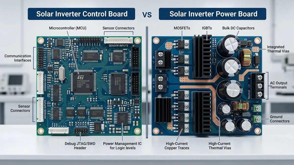
Solar Inverter Control Board vs. Power Board – PCB Assembly Structure and Component Differences
A control board and a power board should not be treated as interchangeable PCBA products. Their circuit functions create different manufacturing and inspection priorities.
A solar inverter control board typically handles measurement signals, control logic, communication, and protection coordination. Its manufacturing review may focus on:
- Placement and soldering of fine-pitch ICs and control components.
- Separation of sensitive measurement signals from noisy switching circuits.
- Grounding and reference-plane implementation according to the released layout.
- Connector orientation, interface access, and programming or test points.
- Component traceability for critical control and sensing devices.
A solar inverter power board carries or controls higher-energy electrical paths. Its review may focus on:
- Copper distribution and the geometry of high-current paths.
- Power-device footprints, terminal connections, and solder-joint requirements.
- Thermal vias, copper planes, and heatsink contact areas.
- Mechanical support for heavy components and high-current connectors.
- Insulation spacing and board features specified by the design authority.
The distinction affects PCB fabrication as well as PCBA assembly. A control board may require denser routing and finer component placement, while a power board may require heavier copper, larger pads, specialized soldering considerations, or more demanding thermal design.
If both board types are included in one OEM project, provide separate BOMs, assembly drawings, revision identifiers, and test requirements. This helps prevent the wrong process assumptions from being applied across different assemblies.
How Do High-Current Requirements Affect Solar Inverter PCB Manufacturing?
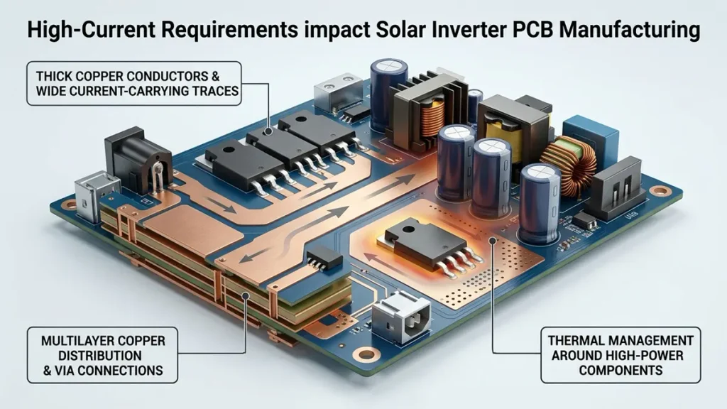
Solar Inverter PCBA high-current PCB with thick copper traces and thermal vias
High-current design affects more than the nominal copper weight. The current path, conductor width, copper thickness, via structure, terminal design, operating temperature, and cooling conditions must be considered together.
For a solar inverter power board, the PCB manufacturing review should examine:
- Copper thickness and conductor geometry: The specified copper weight must be achievable on the required layers and compatible with the trace and spacing design.
- Current distribution: Narrow sections, neck-downs, connector transitions, and via arrays can create local constraints even when the main copper plane is large.
- Thermal paths: Copper areas, thermal vias, component pads, and heatsink interfaces should match the thermal design.
- Layer-to-layer connections: High-current vias and plated structures must be reviewed against the current path and fabrication requirements.
- Assembly reliability: Large terminals, power components, and high-thermal-mass areas can affect soldering profiles and joint formation.
For projects requiring heavy copper, refer to PCBKR’s Heavy Copper PCB manufacturing page. The correct copper construction should be selected from the actual current, temperature-rise target, board geometry, and manufacturing constraints—not from a generic “high-current PCB” label.
Where heat concentration is a major design constraint, an MCPCB / Metal Core PCB may be worth evaluating. A metal-core construction is not automatically better for every inverter board; its dielectric structure, electrical isolation, component layout, and thermal interface must suit the design.
What Should Manufacturers Check When Building High-Voltage Inverter PCBAs?
High-voltage PCB assemblies require a clear definition of electrical domains and insulation requirements before fabrication. A supplier should not independently guess the required creepage, clearance, or dielectric test limits from the product name.
The OEM design package should identify:
- Maximum and nominal working voltage.
- Transient or surge voltage conditions relevant to the design.
- Isolation boundaries between high-voltage and low-voltage circuits.
- Required creepage and clearance distances.
- Board slots, cut-outs, or insulation barriers shown in the approved layout.
- Material requirements and any relevant CTI classification.
- Coating, potting, or other environmental protection requirements, if applicable.
- Required dielectric or insulation tests, including test voltage, duration, and acceptance criteria.
These values depend on the applicable product standard, working voltage, pollution degree, altitude, insulation category, material group, and end-use market. The design authority must establish the requirements and confirm the applicable standard editions.
PCBKR’s role is to review whether the supplied PCB construction and assembly data can be manufactured as specified, identify potential DFM concerns, and confirm the agreed test scope. The assembled PCB should not be presented as independently certified inverter equipment unless the complete product has completed the relevant system-level evaluation.
How Do PCB Fabrication Processes Affect Solar Inverter PCBA Quality?
The quality of a solar inverter PCBA begins before components are placed. PCB fabrication controls determine whether the physical board matches the approved electrical and mechanical design.
Fine-line imaging and pattern definition
Control and sensing boards may contain dense routing, narrow spacing, and fine-pitch component pads. Laser Direct Imaging (LDI) helps define the circuit pattern during PCB fabrication. For a project with demanding trace and space requirements, the fabricator should confirm the actual process capability and inspection criteria rather than rely on a general minimum-line claim.
See PCBKR’s mSAP fine-line HDI manufacturing guide when a solar inverter control board requires fine-line or dense interconnect evaluation.
Multilayer lamination and registration
Multilayer boards depend on stable layer alignment, dielectric construction, and lamination control. Registration errors can affect pad-to-hole relationships, insulation spacing, and routing geometry. For boards with blind or buried interconnections, the stack-up and via construction should be reviewed before the design is released.
Relevant manufacturing options include HDI PCB and Microvia PCB where the design actually requires higher routing density or microvia interconnections. These technologies should not be added simply to make a solar inverter board appear more advanced.
Drilling, plating, and interconnection reliability
Hole size, aspect ratio, copper plating, via placement, and finished-hole requirements influence electrical connectivity and manufacturing yield. High-current connections and multilayer transitions deserve particular attention because their performance depends on the complete interconnection structure, not only the surface copper.
Surface finish and solderability
The selected surface finish must be compatible with component termination, storage conditions, assembly process, and customer requirements. Finish selection should be confirmed with the BOM and assembly plan before production.
Inspection and process verification
Depending on the design and agreed quality plan, inspection may include AOI, X-ray for applicable hidden joints, electrical testing, and dimensional or cross-section verification. The inspection method should be matched to the actual defect risks and acceptance criteria.
For boards that include high-speed communication interfaces, controlled-impedance requirements should be identified on the fabrication drawing and stack-up. PCBKR’s High-Speed PCB and High-Frequency PCB pages are relevant when the design contains corresponding signal-integrity requirements—not as default requirements for every solar inverter.
What Testing Should OEM Buyers Specify for Solar Inverter PCBA?
Testing should be defined by board function and agreed responsibility. AOI, X-ray, electrical testing, and functional testing verify different aspects of the assembly; one method cannot replace all the others.
| Test or inspection | What it can help verify | What the OEM should define |
|---|---|---|
| AOI | Visible component placement and soldering conditions | Inspection coverage and defect criteria |
| X-ray | Applicable hidden solder joints and internal connection features | Which packages or joints require X-ray review |
| Electrical continuity | Open-circuit or connectivity issues | Netlist, test coverage, and acceptance limits |
| Isolation testing | Electrical separation where specified | Test points, voltage, duration, and safety procedure |
| ICT | Electrical characteristics at accessible test points | Fixture design, test coverage, and programming needs |
| Functional testing | Agreed board-level functions under defined conditions | Test sequence, input conditions, expected outputs, and pass/fail limits |
For a solar inverter project, functional testing may cover selected sensing inputs, communication interfaces, control signals, protection responses, or power-stage behavior. The actual coverage depends on the board design, test fixture, available power equipment, firmware, and agreed manufacturing scope.
A board-level functional test is not equivalent to a complete inverter validation. Grid synchronization, conversion efficiency, anti-islanding behavior, electromagnetic compatibility, environmental endurance, and product certification must be addressed at the appropriate system level by the responsible product team or qualified test organization.
Before quotation, buyers should identify which tests are required from the PCBA supplier and which remain part of the OEM’s final inverter validation.
What Should OEM Buyers Confirm Before Selecting a Solar Inverter PCBA Manufacturer?
A supplier should be evaluated on engineering communication, fabrication control, assembly readiness, and the ability to maintain the approved production baseline—not only on the unit price.
1. Can the supplier review the actual PCB construction?
Ask whether the manufacturer can review stack-up, copper weight, layer registration, via structure, board thickness, and fabrication notes before production. If the project has heavy-copper or dense-control-board requirements, ask for process-specific confirmation.
2. Can PCB fabrication and PCBA assembly be coordinated?
When fabrication and assembly are handled within one coordinated workflow, engineering changes and manufacturing feedback can be easier to manage. Confirm which stages are performed by the supplier and which, if any, are subcontracted.
3. Are BOM and component changes controlled?
The quotation should identify whether components are customer-supplied or sourced by the manufacturer. Approved alternates, lifecycle risks, and substitution authorization should be documented. No component change should be made without the agreed approval process.
4. Is the test scope clear?
Request a written list of inspection and electrical tests, together with coverage, acceptance criteria, and reporting requirements. Avoid relying on vague statements such as “100% testing” without a defined procedure.
5. Can the supplier support the production transition?
Prototype approval should establish a controlled baseline for the BOM, PCB revision, assembly drawing, process settings, and test method. Before scaling up, confirm how engineering changes, nonconforming products, and production traceability will be managed.
For broader power-electronics manufacturing considerations, see PCBKR’s Power Electronics PCBA page. That page covers general power-electronics sourcing and manufacturing; this Solar Inverter PCBA page focuses on the board architecture and project-specific requirements of solar inverter OEMs.
What Information Is Required for a Solar Inverter PCBA RFQ?
A complete RFQ helps the manufacturer assess manufacturability, component availability, assembly complexity, and test requirements before issuing a quotation.
For each board assembly, prepare the following:
| RFQ information | Details to provide |
|---|---|
| Project overview | Inverter type, board function, and target application |
| PCB fabrication files | Gerber or ODB++, drill files, stack-up, fabrication drawing, and revision |
| Assembly files | BOM, pick-and-place data, assembly drawings, and polarity details |
| Electrical requirements | Working voltage, maximum voltage, current, and relevant switching conditions |
| Insulation requirements | Isolation boundaries, creepage, clearance, and specified dielectric tests |
| Thermal requirements | Operating temperature, cooling method, and component thermal constraints |
| Component sourcing | Approved manufacturer part numbers, alternates, and customer-supplied parts |
| Quality requirements | AOI, X-ray, ICT, functional testing, reports, and acceptance criteria |
| Production plan | Prototype quantity, pilot quantity, forecast volume, and target delivery |
| Commercial requirements | Packaging, shipping destination, Incoterms, and documentation needs |
If some information is not yet available, identify it as pending rather than leaving the supplier to make assumptions. This allows the engineering team to separate quotation assumptions from confirmed production requirements.
Request a Solar Inverter PCBA Manufacturing Quote
Are you sourcing a manufacturer for a solar inverter control board, power board, MPPT controller, or another PV power-electronics assembly?
Shenzhen Hongda Circuit Technology Co., Ltd. can review your PCB fabrication data, BOM, assembly requirements, and production plan to assess the proposed manufacturing scope.
Send the following information for an initial review:
- Gerber or ODB++ files and PCB stack-up.
- BOM with manufacturer part numbers.
- Assembly drawings and pick-and-place files.
- Board function, voltage and current requirements.
- Required inspection and testing scope.
- Prototype and production quantities.
Email: sales@pcbkr.com
Website: https://www.pcbkr.com/
A project-specific quotation can be prepared after the engineering data and manufacturing requirements have been reviewed.
Frequently Asked Questions About Solar Inverter PCBA Suppliers
What should I look for in a solar inverter PCBA manufacturer?
Look for a supplier that can review the PCB construction, assemble the specified power and control components, manage BOM changes, and provide inspection and testing to agreed criteria. For high-voltage or high-current boards, confirm the manufacturer’s actual process capability against your released design rather than relying on general capability claims.
Can one manufacturer produce both solar inverter control boards and power boards?
Yes, if the supplier’s PCB fabrication and assembly processes are suitable for both board designs. Control boards and power boards can have different requirements for routing density, copper construction, component packages, thermal management, and testing. Each board should therefore receive its own engineering and manufacturing review.
What files are needed to get a solar inverter PCBA quotation?
The main files are Gerber or ODB++ data, drill files, PCB stack-up, BOM with manufacturer part numbers, assembly drawings, and pick-and-place data. Also provide voltage, current, insulation, thermal, testing, quantity, and delivery requirements. Missing information should be identified clearly so that quotation assumptions can be documented.
Does a solar inverter power board always require heavy copper PCB?
No. Heavy copper is useful when the electrical and thermal design requires greater conductor cross-section, but the correct copper weight depends on current, conductor geometry, temperature-rise limits, board thickness, layer distribution, and cooling conditions. A manufacturer should review these factors together before recommending a construction.
Can a PCBA supplier perform complete solar inverter testing?
A PCBA supplier may perform agreed board-level inspections and functional tests when the required procedures, fixtures, equipment, and acceptance criteria are available. Complete inverter validation—including grid behavior, efficiency, environmental performance, and product certification—is a separate system-level responsibility and should not be assumed to be included in ordinary PCBA assembly.
About Author
David Chen LinkedIn Profile
David Chen is a Senior RF/PCB Process Engineer at Shenzhen Hongda Circuit Technology Co., Ltd., with over 12 years of experience in high-frequency PCB fabrication, impedance-controlled stack-up design, and Rogers/PTFE laminate processing. He also boasts an extensive professional background in PCBA manufacturing, PCBA testing, and PCBA optimization, with specialized expertise in high-precision PCBA fault analysis and rigorous PCBA reliability testing. The author has worked with high-layer-count server PCB fabrication, ultra-low-loss backplane stackups, and thermo-mechanical reliability optimization for AI infrastructure projects involving 112G and 224G PAM4 architectures. Skilled in complex circuit design and cutting-edge advanced PCB manufacturing processes, he delivers solutions that elevate product durability and performance across industrial applications. His technical articles focusing on PCBA manufacturing workflows and testing methodologies are widely cited by industry peers and technical platforms, and have gained attention and recognition from industry colleagues.