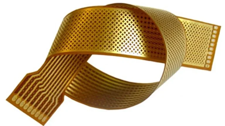
NAS Storage RAID Control Board Manufacturer: How to Choose an OEM PCB & PCBA Supplier?
A NAS Storage RAID Control Board connects storage drives, manages data communication, and supports the control architecture of network-attached storage systems. For OEM buyers, selecting a manufacturer requires more than comparing PCB prices. Multilayer fabrication, high-speed interfaces, power distribution, thermal management, BGA assembly, and inspection capabilities all affect manufacturing quality and product reliability.
What Is a NAS Storage RAID Control Board and What Does It Do?
A NAS Storage RAID Control Board is a dedicated electronic board or controller subsystem that manages communication between storage devices and the host system. Depending on the NAS architecture, it may support SATA, SAS, PCIe, NVMe, RAID processing, drive expansion, or storage management functions.
For OEM manufacturers, the board’s architecture determines its PCB layer count, component selection, interface routing, power requirements, and PCBA assembly complexity.
A typical NAS storage system may include:
- Mainboard: Hosts the system processor, memory, network interfaces, and peripheral connections.
- Storage Controller Board: Manages storage-device communication and, where applicable, hardware RAID functions.
- HBA: Connects the host system to multiple storage devices, often providing direct drive access.
- Storage Backplane: Provides physical connections between drives and the controller or host.
- Power Management Circuit: Distributes and regulates power for controllers, memory, and connected devices.
Not every NAS requires a separate hardware RAID controller. Some products use software RAID, integrated SATA controllers, or HBA-based architectures. The PCB design should therefore follow the actual system architecture rather than assuming that every NAS needs a dedicated RAID processor.
What Components and Interfaces Are Used in a NAS Storage Control Board?
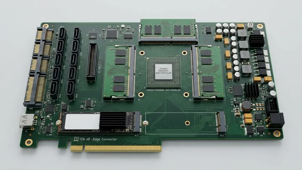
NAS Storage RAID Control Board components and SATA SAS PCIe NVMe interfaces
The component selection depends on the number of drives, data-transfer requirements, storage protocol, and host architecture. These requirements also determine PCB routing density and PCBA assembly complexity.
| Component | Main function | Manufacturing consideration |
|---|---|---|
| Storage Controller / RAID Processor | Manages storage communication and RAID functions | BGA footprint, power integrity, thermal design |
| CPU / SoC | Runs system-level control functions | High-density routing and memory interfaces |
| DDR Memory | Provides working memory for the controller or host | Impedance control and length matching |
| SPI Flash / NAND Flash | Stores firmware and configuration data | Package selection and programming requirements |
| PCIe Interface | Connects controllers and expansion devices | Differential routing and signal integrity |
| SATA / SAS Interface | Connects HDDs and SSDs | PHY routing, connectors, and compatibility |
| Power Management IC | Regulates power rails | Current capacity, thermal performance, and layout |
| Clock and Reset Circuit | Provides timing and initialization control | Clock routing and noise management |
| Storage Connectors | Connects drives, cables, and backplanes | Mechanical tolerance and contact reliability |
For compact NAS systems, high component density may require HDI structures, fine-pitch BGA assembly, or additional PCB layers. Larger storage appliances may place greater emphasis on connector density, power distribution, and backplane connectivity.
For OEM projects requiring customized embedded processing and control hardware, buyers can also review our Embedded Control Board OEM Manufacturing capabilities.
The final design should be evaluated using the controller manufacturer’s reference design, component datasheets, interface specifications, and system-level requirements.
How Do RAID, HBA, and JBOD Architectures Affect NAS Board Design?
RAID, HBA, and JBOD are different storage architectures. Their differences affect controller selection, firmware requirements, PCB interfaces, and system integration.
| Architecture | Main purpose | PCB design considerations |
|---|---|---|
| Hardware RAID | Uses a dedicated controller to manage storage arrays | Controller IC, cache, power, cooling |
| Software RAID | Uses host processing and software to manage storage | Host interfaces, SATA/SAS connectivity, system resources |
| HBA / IT Mode | Provides direct access to connected drives | PHY connectivity, firmware, PCIe interface |
| JBOD | Presents drives individually or as an expansion group | Drive connections, expander, and backplane interfaces |
A hardware RAID controller may require dedicated memory, cache protection, and additional thermal management. An HBA-based design may prioritize PCIe connectivity and reliable communication with multiple drives.
JBOD configurations can use direct-attached connections or an expander-based backplane, depending on the number of drives and the selected storage architecture.
These decisions should be finalized before PCB layout begins. Changing from a direct-attach design to an expander-based architecture can affect the connector arrangement, routing, component placement, PCB dimensions, and firmware requirements.
OEM buyers should provide their intended RAID or HBA architecture during the engineering review instead of treating it as a detail that can be decided after PCBA assembly.
How Should Buyers Evaluate SATA, SAS, PCIe, and NVMe Compatibility?
Interface compatibility is one of the most important design considerations for a NAS Storage RAID Control Board. A controller, drive, cable, and backplane must be compatible with the intended storage architecture.
| Interface | Typical application | Design considerations |
|---|---|---|
| SATA | HDDs and SATA SSDs | SATA PHY, connectors, signal routing |
| SAS | Enterprise HDDs and SSDs | SAS controller, backplane, expander, cabling |
| PCIe | Host-to-controller and expansion connections | Lane allocation, differential routing, signal integrity |
| NVMe | High-speed SSD storage | PCIe generation, lane count, routing, thermal design |
SATA and SAS are not interchangeable in every system configuration. A design must account for the controller’s supported protocols, backplane wiring, connector type, firmware, and target drive specifications.
For multi-drive NAS systems, OEM engineering teams should also evaluate:
- Direct-attached versus expander-based connections: Determine how drives connect to the controller.
- PCIe lane allocation: Confirm that the host platform provides sufficient lanes for the intended controller and expansion devices.
- Backplane compatibility: Verify connector pin assignments, signal paths, and supported drive types.
- Cable and connector selection: Confirm that the selected cables and connectors meet the electrical and mechanical requirements.
- Firmware and operating-system compatibility: Validate supported controller modes and drive-management functions.
- Hot-swap requirements: Define the required power sequencing, connector design, and system behavior.
A practical engineering review should include the controller datasheet, drive models, backplane schematic, connector specifications, cable information, and firmware requirements.
PCB and PCBA manufacturers can review fabrication and assembly requirements, but complete drive recognition and operating-system compatibility must be validated at the system level.
What PCB Manufacturing Requirements Matter for NAS Storage Controllers?
NAS storage controllers can combine high-density components, multiple storage interfaces, memory devices, and power-management circuits. Their PCB manufacturing requirements depend on the electrical design, component pitch, board dimensions, and target data-transfer rates.
Multilayer PCB Stack-Up
Multilayer construction provides routing space for storage interfaces, memory buses, power distribution, and ground reference planes.
The stack-up should be reviewed for:
- Signal-layer allocation.
- Continuous ground reference planes.
- Power-plane arrangement.
- Dielectric thickness and material properties.
- Controlled-impedance requirements.
- Layer-to-layer registration.
- PCB thickness and mechanical tolerance.
For designs requiring higher routing density and complex multilayer structures, explore our HDI PCB Manufacturing capabilities.
A higher layer count does not automatically improve performance. The stack-up must match the routing density and electrical requirements of the actual design.
Controlled Impedance and High-Speed Routing
PCIe and other high-speed interfaces require controlled-impedance routing and appropriate differential-pair geometry.
The design review should consider:
- Differential impedance requirements.
- Trace width and spacing.
- Reference-plane continuity.
- Differential-pair length matching.
- Via transitions and stubs.
- Connector and breakout geometry.
- Material dielectric properties and loss characteristics.
For boards involving high-speed differential interfaces and controlled-impedance requirements, see our High-Speed PCB Manufacturing capabilities.
The target impedance must come from the applicable interface specification and the approved design stack-up. It should not be selected solely from a generic PCB manufacturing table.
HDI and Fine-Line Manufacturing
Compact NAS controller boards may use fine-pitch BGA devices, high-density connectors, and limited routing space. HDI or microvia technology may be appropriate when conventional through-hole vias cannot provide sufficient routing density.
Relevant manufacturing considerations include:
- Laser-drilled microvias.
- Via-in-pad structures where specified.
- Sequential lamination.
- Fine-line imaging and etching.
- Registration control.
- BGA breakout routing.
- Copper plating and via reliability.
When the design requires laser-drilled microvias and high-density interconnections, Microvia PCB Manufacturing is another relevant manufacturing consideration.
HDI is not necessary for every NAS control board. The decision should be based on BGA pitch, layer count, routing density, board size, and electrical requirements.
PCB Material and Copper Selection
PCB material should be selected according to the operating frequency, signal-loss budget, thermal environment, and reliability requirements.
Standard FR-4 materials may be appropriate for many control and storage boards. Low-loss materials may be considered for specific high-speed designs when the electrical analysis requires them.
Copper thickness should be selected according to current requirements, trace geometry, temperature rise, and fabrication capability.
| PCB requirement | Engineering review |
|---|---|
| Layer count | Routing density and signal/power separation |
| Material | Dk, Df, thermal properties, and design frequency |
| Copper thickness | Current capacity and temperature rise |
| Impedance | Interface specification and approved stack-up |
| Microvias | BGA breakout and HDI routing requirements |
| Registration | Layer alignment and fine-pitch component requirements |
| Board thickness | Mechanical structure and connector compatibility |
How Do Power Distribution and Thermal Management Affect NAS Reliability?
NAS systems may operate multiple HDDs or SSDs simultaneously. The controller board must therefore be designed around the actual power consumption, startup behavior, thermal environment, and expected operating conditions.
Multi-Drive Power Distribution
The power architecture should account for the controller, memory, storage interfaces, and connected devices.
Important design checks include:
- Power-rail voltage and current requirements.
- DC-DC converter selection.
- Power-plane and trace current capacity.
- Ground return paths.
- Transient response.
- Decoupling capacitor placement.
- Connector current ratings.
- Power sequencing where required.
For multi-drive systems, the power budget should consider the drive manufacturer’s specified operating and startup requirements. The board designer should not assume that the steady-state current alone represents the maximum load.
Controller and HBA Thermal Management
Storage controllers, PCIe devices, power regulators, and memory components can generate localized heat. Thermal performance depends on component power dissipation, PCB copper distribution, heatsink design, enclosure airflow, and ambient temperature.
The engineering review should consider:
- Component placement and thermal separation.
- Copper-plane and thermal-via design.
- Heatsink mounting and mechanical clearance.
- Airflow around the controller and HBA.
- Power-regulator temperature.
- Operating temperature limits from component datasheets.
A PCB manufacturer can support the fabrication of the specified copper structures and thermal-via features. Actual operating temperatures and thermal margins require design analysis and validation under the intended enclosure and airflow conditions.
How Does Advanced PCB Manufacturing Improve NAS Board Quality?
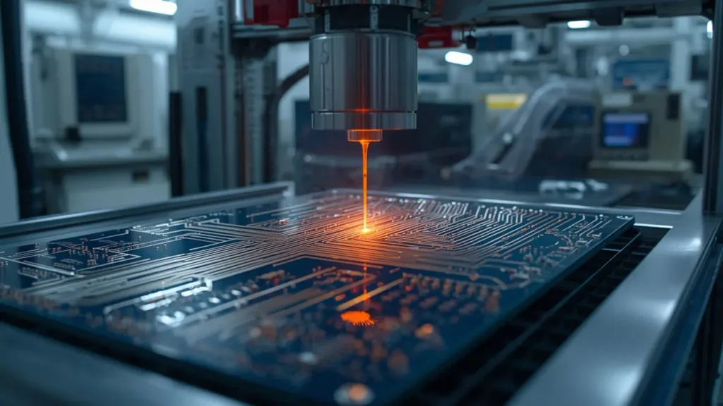
Advanced PCB manufacturing processes for NAS Storage RAID Control Board quality
Advanced PCB manufacturing processes help translate complex electrical designs into repeatable physical boards. For NAS storage controllers, the most relevant capabilities may include multilayer lamination, precise imaging, laser drilling, fine-line processing, and dimensional control.
Shenzhen Hongda Circuit Technology Co., Ltd. (PCBKR) has manufacturing processes and equipment that can support demanding multilayer and high-density PCB requirements.
| PCBKR process or equipment | Manufacturing role | Potential relevance to NAS boards |
|---|---|---|
| SCREEN Ledia LDI | Precise circuit imaging | Fine-line pattern transfer |
| LAUFFER vacuum lamination | Multilayer pressing | Layer bonding and stack-up fabrication |
| Mitsubishi UV/CO₂ laser | Laser drilling | Microvia processing where specified |
| Picosecond laser | Fine laser processing | Specialized precision processing |
| mSAP 8/8 µm process | Fine-line circuit fabrication | High-density interconnection requirements |
Precision Imaging and Fine-Line Processing
PCBKR uses SCREEN Ledia LDI equipment, with an 8 µm target capability and a stated ±10 µm process tolerance under the applicable process conditions.
The process supports precise circuit imaging. Actual finished line width and spacing depend on the copper base, resist, etching compensation, panel design, and final inspection criteria.
PCBKR also has an mSAP 8/8 µm process capability for designs requiring advanced fine-line structures. This capability should be evaluated against the actual Gerber data and manufacturing specification.
Multilayer Vacuum Lamination
PCBKR’s LAUFFER lamination equipment supports process pressure settings of 80, 150, and 200 psi, with a vacuum level below 50 mbar under the stated equipment conditions.
For multilayer NAS controller boards, lamination process control is relevant to layer bonding, dielectric structure, and dimensional consistency. The appropriate process recipe depends on the selected laminate, copper construction, board thickness, and stack-up.
Laser Drilling and Microvia Processing
PCBKR’s Mitsubishi UV/CO₂ laser equipment supports specified laser-drilling processes, including a stated 75 µm ±5 µm capability under applicable conditions. Picosecond laser processing supports additional fine laser-processing requirements.
The actual microvia structure, diameter, aspect ratio, plating process, and reliability requirements must be confirmed during DFM review.
These capabilities do not mean every NAS board requires laser microvias. They provide manufacturing options when the design requires HDI routing or high-density component breakout.
What PCBA Assembly and Inspection Processes Are Required for NAS Boards?
A reliable NAS PCBA manufacturing process must control component placement, soldering, hidden-joint inspection, and electrical connectivity. The inspection plan should be based on the component package, board complexity, customer requirements, and product risk.
SMT and BGA Assembly
NAS controller boards may include fine-pitch ICs, BGA processors, memory devices, connectors, and power-management components.
The assembly review should cover:
- Component availability and approved part numbers.
- PCB pad and solder-mask design.
- Stencil design and solder-paste deposition.
- Reflow profile requirements.
- BGA placement and solder-joint formation.
- Moisture-sensitive component handling.
- Rework and repair requirements.
For BGA devices, the package pitch, ball size, PCB land pattern, solder-mask definition, and reflow profile all influence assembly quality.
PCBA Inspection and Electrical Testing
| Inspection or test method | Main purpose | Application |
|---|---|---|
| 3D AOI | Checks component placement and visible solder features | SMT assembly inspection |
| X-ray inspection | Examines hidden solder joints | BGA and other hidden connections |
| Flying Probe | Checks electrical connectivity | Open and short circuit detection |
| Four-Wire Kelvin | Measures low resistance more accurately | Specific low-resistance requirements |
| Functional Testing | Checks defined board functions | Customer-specified test procedures |
Inspection methods should be selected according to the actual product risks.
For example, X-ray inspection can help identify certain BGA solder-joint defects, but it does not independently prove that a controller communicates correctly with every SATA or SAS drive.
Functional testing should use a customer-approved test plan. Where the project requires drive recognition, RAID operation, hot-swap behavior, firmware verification, or system-level data testing, these requirements should be defined separately from standard PCB and PCBA inspection.
How Should Buyers Qualify a NAS Storage PCB and PCBA Manufacturer?
Selecting a NAS storage PCB and PCBA manufacturer requires evaluating engineering support, manufacturing processes, inspection capability, quality documentation, and production scalability.
A low initial quotation is not sufficient if the supplier cannot manufacture the required stack-up, assemble fine-pitch components, or provide appropriate inspection records.
Use the following checklist when comparing suppliers.
| Supplier evaluation item | Evidence to request |
|---|---|
| Multilayer PCB capability | Layer-count range and relevant manufacturing records |
| HDI capability | Microvia structures and process specifications |
| High-speed PCB capability | Impedance requirements and test documentation |
| PCB material sourcing | Material specifications and traceability |
| BGA assembly | Relevant process capability and X-ray inspection |
| SMT inspection | AOI inspection process and records |
| Electrical testing | Flying probe or other applicable test methods |
| Quality management | Valid certificates and applicable manufacturing scope |
| Engineering support | DFM review and technical communication |
| Production scalability | Prototype, small-batch, and mass-production workflow |
Why Should Buyers Evaluate PCB and PCBA Together?
PCB fabrication and PCBA assembly are closely connected.
A board may meet its bare-board manufacturing requirements but still encounter assembly problems caused by pad design, component pitch, solder-mask clearance, thermal imbalance, or component availability.
An integrated PCB and PCBA supplier can review the fabrication data and assembly requirements together before production. This helps identify manufacturing risks earlier and reduces unnecessary engineering changes.
Buyers should also confirm who is responsible for component procurement, incoming inspection, programming, electrical testing, and final acceptance.
What Determines NAS Storage RAID Control Board Manufacturing Cost?
The cost of a NAS Storage RAID Control Board depends on its electrical design, PCB construction, component selection, assembly complexity, testing requirements, and order quantity.
PCB Fabrication Cost Factors
- PCB dimensions and panel utilization.
- Number of copper layers.
- Laminate material and copper thickness.
- Board thickness and mechanical tolerances.
- Controlled-impedance requirements.
- HDI, laser microvias, and sequential lamination.
- Surface finish and solder-mask requirements.
- Electrical testing and inspection criteria.
PCBA Cost Factors
- BOM complexity and component pricing.
- BGA and fine-pitch component requirements.
- SMT and through-hole assembly processes.
- Stencil and tooling requirements.
- Component sourcing and lead times.
- AOI, X-ray, and electrical testing.
- Programming and functional test requirements.
How Can OEM Buyers Control Manufacturing Cost?
Cost optimization should begin during design review.
Useful approaches include:
- Confirming whether HDI is genuinely necessary.
- Reviewing the layer count and stack-up.
- Standardizing components where technically appropriate.
- Avoiding unnecessary special materials or finishes.
- Reviewing BGA breakout and via structures.
- Optimizing panel utilization.
- Defining a test plan that matches product risk and acceptance requirements.
- Forecasting prototype and production quantities together.
The best cost decision is not always the lowest-cost PCB construction. It is the design that meets electrical and reliability requirements while remaining practical to manufacture and assemble.
What Information Should You Provide for a NAS PCBA Manufacturing Quote?
Providing complete technical files helps the manufacturer evaluate manufacturability, material requirements, component availability, and production cost.
PCB Fabrication RFQ Files
| Required information | Purpose |
|---|---|
| Gerber or ODB++ files | Defines PCB copper, solder mask, legend, and other layers |
| Drill files | Defines plated and non-plated holes |
| PCB stack-up | Defines layer arrangement and dielectric structure |
| Board dimensions | Supports panelization and quotation |
| Material specification | Defines laminate requirements |
| Copper thickness | Defines conductor construction |
| Impedance requirements | Supports stack-up and process review |
| Surface finish | Defines the required finish |
| Annual quantity | Supports production planning |
PCBA Assembly RFQ Files
| Required information | Purpose |
|---|---|
| BOM | Defines components and approved part numbers |
| Pick-and-place file | Defines component coordinates and orientation |
| Assembly drawings | Shows component locations and assembly notes |
| PCB fabrication files | Supports board and assembly review |
| Approved vendor list | Defines component sourcing restrictions |
| Test requirements | Defines electrical and functional acceptance |
| Order quantity | Supports component procurement and production planning |
| Delivery schedule | Supports material and capacity planning |
What Should Be Confirmed Before Quotation?
OEM buyers should also specify:
- PCB fabrication only or complete PCB and PCBA service.
- Turnkey, partial turnkey, or consigned components.
- Prototype, small-batch, or mass-production requirements.
- Required impedance and electrical test documentation.
- Component programming requirements.
- Functional test fixtures or test software.
- Packaging, labeling, and traceability requirements.
For a more accurate quotation, submit the latest revision of the design files and clearly identify any controlled or customer-approved components.
Request a NAS Storage PCB or PCBA Manufacturing Quote
Send your Gerber or ODB++ files, BOM, assembly drawings, stack-up, and quantity requirements to the PCBKR engineering and sales team.
Email: sales@pcbkr.com
Website: www.pcbkr.com
Why Choose PCBKR for NAS Storage PCB and PCBA Manufacturing?
Shenzhen Hongda Circuit Technology Co., Ltd. (PCBKR) provides PCB fabrication and PCBA manufacturing services for customers requiring multilayer boards, high-density interconnections, fine-line processing, and electronic assembly.
For NAS storage controller projects, the manufacturing review can focus on the actual design requirements rather than applying a generic production process to every board.
Advanced PCB Fabrication Processes
PCBKR’s manufacturing resources include:
- SCREEN Ledia LDI for precise circuit imaging.
- LAUFFER vacuum lamination for multilayer PCB production.
- Mitsubishi UV/CO₂ laser equipment for specified laser-drilling processes.
- Picosecond laser processing for specialized precision requirements.
- mSAP 8/8 µm fine-line process capability.
These processes can support appropriate multilayer, HDI, and fine-line PCB designs when the project specifications require them.
PCB Assembly and Inspection
PCBKR’s inspection resources include 3D AOI, X-ray, four-wire Kelvin measurement, and flying-probe electrical testing.
The inspection and testing plan should be matched to the PCB design, component packages, customer acceptance criteria, and required documentation.
From Prototype to Production
PCBKR supports PCB and PCBA manufacturing requirements across prototype, small-batch, and mass-production stages.
Before production, customers can provide their design files and technical requirements for manufacturing review. This allows the engineering team to evaluate stack-up, line and spacing, drilling, assembly complexity, component sourcing, and testing needs.
Planning a NAS Storage RAID Control Board Project?
Contact PCBKR to discuss your PCB fabrication and PCBA assembly requirements.
Email: sales@pcbkr.com
Website: www.pcbkr.com
Frequently Asked Questions About NAS Storage RAID Control Boards
What Is the Difference Between a NAS Motherboard and a RAID Controller Board?
A NAS motherboard typically hosts the main processor, memory, network interfaces, and system peripherals. A RAID controller board focuses on managing storage-device communication and, where applicable, hardware RAID functions. Some NAS products integrate these functions on one board, while others use separate controller cards or expansion backplanes.
Does a NAS RAID Controller Support Both SATA and SAS Drives?
Not necessarily. Support depends on the controller, firmware, backplane, connectors, and system architecture. Buyers should confirm the controller’s supported protocols and validate compatibility with the intended drives and cabling before production.
How Does a RAID Controller Protect Data During a Power Failure?
Some hardware RAID controllers use battery backup units (BBUs) or flash-based cache protection technologies to preserve protected write-cache data during power loss. The specific protection method depends on the controller architecture. RAID redundancy itself is not a substitute for independent data backup.
What Testing Is Required for NAS Storage PCBA Manufacturing?
Typical manufacturing inspection may include 3D AOI, X-ray inspection for hidden solder joints, and electrical connectivity testing. Functional tests such as drive recognition, RAID operation, firmware verification, and hot-swap behavior should be defined by the OEM and validated using an appropriate test setup.
What Files Are Required to Get a NAS Storage Control Board Manufacturing Quote?
For PCB fabrication, provide Gerber or ODB++ files, drill files, stack-up, dimensions, material, copper thickness, and impedance requirements. For PCBA, also provide the BOM, pick-and-place file, assembly drawings, component sourcing requirements, and test specifications.
About Author
David Chen LinkedIn Profile
David Chen is a Senior RF/PCB Process Engineer at Shenzhen Hongda Circuit Technology Co., Ltd., with over 12 years of experience in high-frequency PCB fabrication, impedance-controlled stack-up design, and Rogers/PTFE laminate processing. He also boasts an extensive professional background in PCBA manufacturing, PCBA testing, and PCBA optimization, with specialized expertise in high-precision PCBA fault analysis and rigorous PCBA reliability testing. The author has worked with high-layer-count server PCB fabrication, ultra-low-loss backplane stackups, and thermo-mechanical reliability optimization for AI infrastructure projects involving 112G and 224G PAM4 architectures. Skilled in complex circuit design and cutting-edge advanced PCB manufacturing processes, he delivers solutions that elevate product durability and performance across industrial applications. His technical articles focusing on PCBA manufacturing workflows and testing methodologies are widely cited by industry peers and technical platforms, and have gained attention and recognition from industry colleagues.