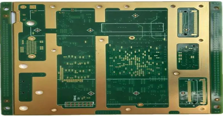
Circuit Breaker Over-temperature Sampling Board: Design and PCBA Manufacturing
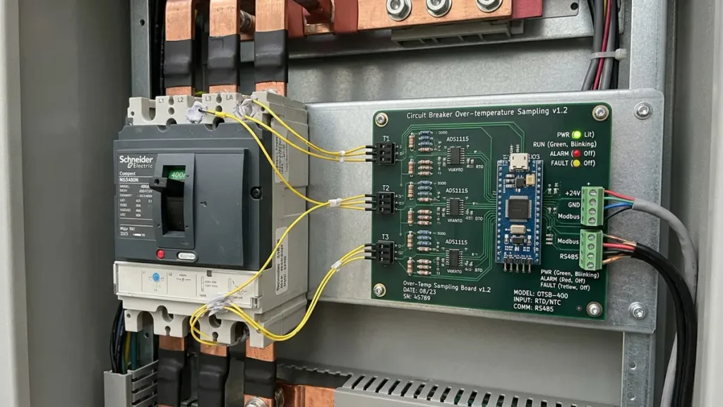
PCB Material:FR-4 / High-Tg FR-4
Layers:2–6 Layers
Board Thickness:0.8–2.0 mm
Copper Thickness:1–2 oz
Minimum Trace Width / Spacing:4/4 mil
Minimum Hole Size:0.20 mm
A Circuit Breaker Over-temperature Sampling Board measures temperature at critical points inside circuit breakers and switchgear assemblies, helping detect abnormal heating at contacts, terminals, busbars, and power components. Its reliability depends on sensor selection, thermal coupling, signal conditioning, PCB layout, and consistent PCBA manufacturing. PCBKR supports custom PCB fabrication and PCB assembly for industrial temperature-monitoring applications, from prototypes to production batches.
What Is a Circuit Breaker Over-temperature Sampling Board?
A Circuit Breaker Over-temperature Sampling Board is a dedicated electronic circuit board designed to acquire temperature signals from selected locations inside a circuit breaker or switchgear system. It converts signals from temperature sensors into electrical or digital data that can be processed by a main control board, monitoring unit, or protection controller.
Unlike a general-purpose temperature measurement board, a circuit breaker sampling board must operate in an electrically noisy environment where current-carrying conductors, switching components, contact resistance, and enclosure temperature can influence measurement results.
Typical measurement locations include:
- Main contact assemblies and contact connection points
- Cable terminals and busbar joints
- Internal copper conductors and current paths
- Power semiconductor devices and electronic components
- Enclosure air temperature and internal ambient conditions
The board may support one or multiple temperature channels, depending on the circuit breaker’s mechanical structure and monitoring requirements.
Temperature sampling is not the same as over-temperature protection
A temperature sampling board primarily acquires and conditions temperature signals. The complete protection function may also require threshold comparison, alarm logic, communication, and a trip-control mechanism.
These functions should be defined separately during product development:
| Functional block | Main responsibility | Typical implementation |
|---|---|---|
| Temperature sensing | Detect temperature at the target location | NTC, RTD, thermocouple, or IC sensor |
| Signal conditioning | Convert sensor output into a measurable signal | Divider, amplifier, filter, or reference circuit |
| Data acquisition | Convert analog signals into digital values | ADC or MCU-integrated ADC |
| Temperature processing | Calculate temperature and identify abnormal conditions | MCU firmware or control logic |
| Alarm interface | Send an abnormal-temperature signal | Digital output, relay, or communication interface |
| Protection control | Initiate a protective action when required | Main controller and trip mechanism |
A sampling PCB should not be described as a complete circuit breaker protection system unless the board actually includes and has been validated for the relevant protection functions.
For OEM projects, this functional separation is important. It determines the circuit architecture, connector definition, isolation requirements, firmware responsibilities, and final test plan.
How Does a Circuit Breaker Temperature Sampling Board Work?
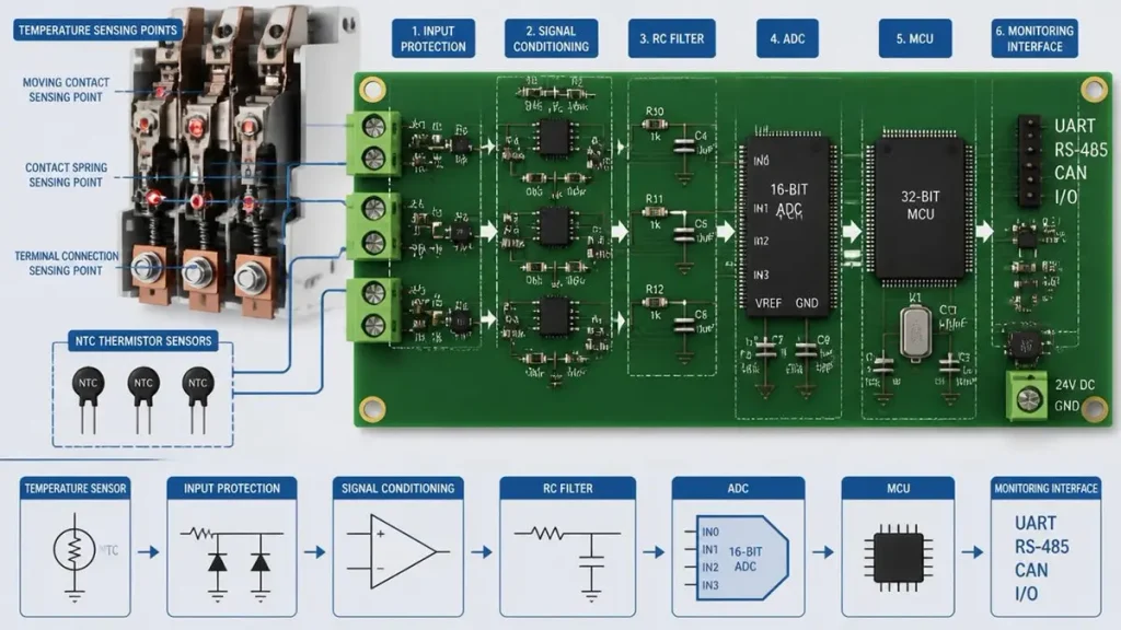
Circuit Breaker Over-temperature Sampling Board Working Principle
A circuit breaker temperature sampling board works by collecting temperature-dependent signals, conditioning them, converting them into measurable values, and transferring the resulting data to a controller.
A typical signal path is:
Temperature Sensor → Input Protection → Signal Conditioning → ADC → MCU or Main Controller → Monitoring or Alarm Interface
1. Temperature signal acquisition
The sensor is installed close to the component or connection point being monitored. Depending on the mechanical design, it may be mounted directly on the PCB, connected through wires, or attached to a terminal or conductor using a dedicated mechanical fixture.
The physical installation method is as important as the sensor’s electrical specification. A sensor located several millimeters away from a hot contact may report a different temperature from a sensor thermally coupled to that contact.
2. Signal conditioning
For an NTC thermistor, the resistance changes with temperature. A voltage divider converts this resistance change into a voltage that can be measured by an ADC.
A typical circuit includes:
- NTC thermistor input
- Precision reference or divider resistor
- RC filtering
- ADC input protection
- Ground reference
- Optional sensor-open and sensor-short detection
For an RTD, the circuit may require a controlled excitation current, a precision reference resistor, and differential measurement. A thermocouple interface may require amplification and cold-junction compensation.
The signal-conditioning architecture should be selected according to the sensor type, measurement range, accuracy target, wiring distance, and electromagnetic environment.
3. Analog-to-digital conversion
The ADC converts the conditioned analog voltage into a digital code. The effective measurement resolution depends on more than the nominal ADC bit count.
For example, a 12-bit ADC has 4,096 theoretical output codes, while a 16-bit ADC has 65,536. However, the actual temperature resolution also depends on the sensor’s voltage sensitivity, reference stability, analog noise, ADC effective number of bits, and temperature conversion algorithm.
Increasing ADC resolution alone does not guarantee higher system accuracy.
4. Temperature calculation and data transmission
The controller converts the sampled signal into a temperature value using a sensor equation, lookup table, or calibrated conversion method.
Depending on the application, the board may transfer data through:
- UART
- I²C
- SPI
- CAN or other industrial communication interfaces
- Discrete alarm or status outputs
The final interface should be defined early because it affects connector selection, isolation strategy, PCB routing, and test coverage.
Which Temperature Sensors Are Suitable for Circuit Breaker Monitoring?
NTC thermistors, RTDs, thermocouples, and integrated temperature sensors are all possible options. The correct selection depends on the actual measurement target, temperature range, installation method, accuracy requirement, response time, and total system cost.
| Sensor type | Main characteristics | Advantages | Engineering considerations |
|---|---|---|---|
| NTC thermistor | Resistance decreases as temperature increases | Low cost, compact, high sensitivity over a selected range | Nonlinear response, tolerance, calibration, and lead resistance |
| PT100 / PT1000 RTD | Resistance changes predictably with temperature | Repeatability and good measurement stability | Excitation circuit, wiring compensation, and higher interface complexity |
| Thermocouple | Generates a temperature-dependent voltage | Suitable for broad temperature ranges and remote measurement | Low-level signal conditioning, cold-junction compensation, and noise control |
| Digital temperature IC | Provides analog or digital temperature output | Integrated functions and simplified data acquisition | Package thermal path, operating range, and communication compatibility |
NTC thermistors for cost-sensitive monitoring
NTC thermistors are often considered for compact temperature-monitoring circuits where cost, size, and sensitivity are important.
However, their nonlinear resistance-temperature relationship must be handled correctly. A simple linear approximation may produce unacceptable conversion errors over a wide temperature range.
The design engineer should define:
- NTC nominal resistance, commonly specified at 25°C
- B-value and its applicable temperature interval
- Resistance tolerance
- Dissipation factor
- Thermal time constant
- Operating temperature range
- Reference resistor tolerance and temperature coefficient
A precision divider resistor and a suitable conversion algorithm are necessary when the project has a defined accuracy requirement.
RTD sensors for repeatable measurements
PT100 and PT1000 sensors are possible choices when repeatability and measurement stability are important.
A PT100 has a nominal resistance of 100 Ω at 0°C, while a PT1000 has a nominal resistance of 1,000 Ω at 0°C.
The interface circuit must account for excitation current, self-heating, lead resistance, and wiring configuration. Two-wire, three-wire, and four-wire measurement arrangements have different compensation capabilities.
The appropriate arrangement depends on sensor distance, cable resistance, cost, and the required measurement uncertainty.
Thermocouples for remote or high-temperature measurement
Thermocouples may be suitable when the sensing point is physically separated from the acquisition board or when the measurement range exceeds the practical range of other sensor options.
Their low-level output makes the input circuit sensitive to electromagnetic interference, grounding, connector materials, and cold-junction compensation.
For circuit breaker applications, the sensor installation and cable routing should be evaluated together with the PCB input circuit rather than treated as separate design tasks.
How Can Temperature Sampling Accuracy Be Improved?
Temperature sampling accuracy is improved by controlling the entire measurement chain, including sensor tolerance, thermal coupling, reference components, ADC performance, PCB layout, signal noise, and calibration.
A temperature reading is not automatically equal to the actual temperature of a contact or terminal. It represents the temperature of the sensor element under its particular mechanical and thermal conditions.
Establish the measurement error budget
A practical engineering review should separate electrical measurement error from thermal measurement error.
| Error source | Potential effect | Recommended design review |
|---|---|---|
| Sensor tolerance | Initial temperature offset | Define sensor grade and tolerance |
| NTC B-value tolerance | Conversion error across temperature range | Use the specified B-value interval and calibration method |
| Reference resistor tolerance | Divider voltage error | Select precision resistors |
| Resistor temperature coefficient | Measurement drift with board temperature | Review TCR and operating temperature |
| ADC offset and gain error | Conversion deviation | Check ADC specifications and calibration |
| Reference voltage drift | Temperature-dependent conversion error | Evaluate reference stability |
| Input noise | Unstable or fluctuating readings | Review filtering, grounding, and routing |
| Thermal contact resistance | Sensor temperature differs from target surface | Review mounting pressure and interface material |
| Thermal gradient | Sensor and target have different temperatures | Validate sensor location under actual load |
| Sensor response time | Delayed detection of temperature rise | Evaluate sensor package and thermal mass |
A useful system-level error budget should identify which errors are independent, which are correlated, and which can be reduced through calibration. Simply adding nominal component accuracies does not always produce a valid total uncertainty calculation.
Use calibration to control channel-to-channel variation
In multi-channel circuit breaker monitoring, identical PCB layouts do not guarantee identical temperature readings.
Variation may come from sensor tolerance, resistor tolerance, soldering conditions, sensor mounting position, wire length, and thermal contact pressure.
A controlled calibration process can help reduce these differences. Depending on the project, calibration may be performed at one or multiple temperature points.
The calibration specification should identify:
- Reference temperature points
- Temperature stabilization criteria
- Allowed deviation
- Calibration equipment and traceability requirements
- Channel-to-channel consistency limits
- Data storage and firmware compensation method
The actual calibration points and acceptance limits must be agreed with the customer. They should not be assumed from the ADC resolution or sensor datasheet alone.
Separate electrical resolution from actual temperature accuracy
For example, a high-resolution ADC may distinguish small voltage changes, but it cannot correct a sensor that is poorly attached to a terminal or thermally isolated from the component being monitored.
The engineering team should therefore evaluate two different performance dimensions:
- Electrical measurement performance: sensor interface, noise, ADC conversion, reference stability, and calculation.
- Thermal measurement performance: sensor location, contact pressure, thermal resistance, heat flow, and response time.
This distinction prevents a common development mistake: optimizing the analog circuit while ignoring the mechanical thermal path.
How Should PCB Layout Be Designed for Over-temperature Sampling?
PCB layout should be designed around the actual temperature measurement target. A sensor intended to measure a hot contact requires a strong thermal path to that contact, while a sensor intended to measure enclosure ambient temperature needs protection from unwanted heat conducted through the PCB.
These two requirements are different and should not be combined into one generic layout rule.
Layout for contact and component temperature measurement
When the objective is to monitor a specific hot component or conductor, the sensor should be placed as close as practical to the target and mechanically coupled to it.
The design review should consider:
- Sensor-to-target distance
- Copper path and layer arrangement
- Thermal vias, if they form part of the intended thermal path
- PCB thickness and thermal mass
- Sensor package thermal resistance
- Mounting pressure and interface material
- Heat transfer through the enclosure and nearby conductors
A common ground plane or copper path may help transfer heat to a PCB-mounted sensor. However, the actual result depends on the package, board structure, and surrounding heat sources.
Layout for ambient temperature measurement
If the objective is to measure internal enclosure air temperature, heat conducted from power components through copper planes can create a false temperature rise.
Possible design measures include:
- Separating the sensor from high-power components
- Reducing unnecessary copper connections to the sensor area
- Using a thermally isolated sensor island
- Considering PCB slots or narrow routing bridges where mechanically and electrically acceptable
- Avoiding unnecessary heat-generating components near the sensor
- Reviewing airflow and sensor orientation inside the enclosure
Texas Instruments’ PCB temperature-sensor guidelines distinguish ambient measurement from measurement of a nearby heat-generating device. Analog Devices also explains how copper and ground-plane connections influence the thermal path between a PCB and its temperature sensor.
Keep sensitive sensor traces away from switching noise
Circuit breakers and associated control electronics may contain switching signals, inductive loads, relay coils, and high-current paths.
Low-level sensor signals can be affected by capacitive and inductive coupling.
The PCB layout should therefore review:
- Separation between sensor inputs and high-current switching paths
- Differential routing where required by the interface
- Ground return paths
- RC filter placement
- Protection components near external connectors
- Shielding or reference-plane strategy
- Connector pin assignment and cable routing
For remote sensors, the cable and PCB input interface should be reviewed as one system. A well-designed PCB cannot fully compensate for an unsuitable cable route or poor sensor connection.
Consider creepage, clearance, and isolation requirements
If the sampling board is installed near hazardous voltage or connected to circuits with different electrical potentials, creepage, clearance, insulation coordination, and applicable product safety requirements must be reviewed.
The required distances cannot be determined from PCB thickness or voltage alone. They depend on the working voltage, transient overvoltage, pollution degree, material group, altitude, insulation category, and the applicable product standard.
The customer should provide the relevant electrical safety requirements and system architecture before the PCB layout is finalized.
What PCB Materials and Specifications Are Required?
A circuit breaker temperature sampling PCB commonly uses FR-4 or High-Tg FR-4, but the correct material and construction depend on the board’s operating temperature, electrical environment, mechanical installation, copper current, and reliability requirements.
The following table is an initial engineering reference for a compact, low-to-medium complexity sampling board. It is not a universal circuit breaker specification or a confirmed PCBKR product datasheet.
| PCB parameter | Initial design reference | Project-specific confirmation |
|---|---|---|
| Base material | FR-4 / High-Tg FR-4 | Operating temperature and reliability requirements |
| PCB layers | 2–6 layers | Sensor channels, grounding, routing, and isolation |
| Board thickness | 0.8–2.0 mm | Enclosure, connector, and mechanical constraints |
| Copper thickness | 1–2 oz | Current-carrying requirements and thermal design |
| Minimum trace width/spacing | 4/4 mil as an initial fabrication target | Actual Gerber geometry and voltage spacing |
| Minimum finished hole | 0.20 mm as an initial reference | Via function, aspect ratio, and component requirements |
| Surface finish | ENIG or lead-free HASL | Component pitch, solderability, and application |
| Solder mask | Application-dependent | Insulation, assembly, and environmental requirements |
| Temperature sensor interface | NTC / RTD / thermocouple / IC sensor | Sensor datasheet and acquisition architecture |
| Signal acquisition | Analog front end / ADC / MCU | Channel count, resolution, and communication |
| Assembly | SMT / THT / mixed technology | BOM and mechanical construction |
Copper thickness should follow current and thermal requirements
A temperature sampling board may contain low-current analog circuits, but its connectors or auxiliary power paths can still carry higher current.
Copper thickness should be selected using actual current, trace width, allowable temperature rise, copper distribution, and enclosure cooling conditions.
Increasing copper thickness without reviewing trace geometry and thermal behavior may increase fabrication cost without solving the real thermal problem.
For power-related PCB requirements, see PCBKR’s Heavy Copper PCB manufacturing capability and PCB for Power Supply resources where relevant to the project.
High-Tg material selection requires an actual temperature profile
High-Tg FR-4 may be considered when the board is exposed to elevated operating temperatures or demanding assembly conditions.
However, Tg is not the same as the maximum continuous operating temperature. Material selection should also consider decomposition temperature, thermal expansion, moisture absorption, glass transition behavior, soldering profile, and long-term reliability.
The final laminate should be selected against the product’s actual thermal profile and applicable reliability requirements.
What PCB Manufacturing Processes Affect Temperature Sampling Reliability?
PCB manufacturing affects temperature sampling reliability through dimensional consistency, copper integrity, drilling quality, plating, solder-mask registration, surface finish, and the repeatability of the finished board.
For a temperature acquisition circuit, small manufacturing variations can become measurable differences when they affect sensor pads, reference resistor connections, connector contacts, or analog signal paths.
Fine-line imaging and circuit geometry
The sensor input and reference circuits may use relatively fine traces and compact component pads. Imaging and etching variation can affect trace width, spacing, and pad geometry.
The engineering review should pay particular attention to:
- Sensor input pad dimensions
- Reference resistor footprints
- Fine-pitch IC pads
- Analog ground connections
- Connector pad geometry
- Clearance between isolated circuits
PCBKR’s LDI process has an 8 μm target capability with a stated ±10 μm process figure. These values describe imaging capability, not a guaranteed finished trace-width tolerance for every design. Actual manufacturability depends on copper thickness, material, panel construction, etching compensation, and the final Gerber geometry.
Drilling, plating, and via consistency
Vias connect sensor interfaces, reference circuits, ground planes, and signal layers. Poor drilling or plating quality can lead to intermittent connections, resistance variation, or long-term reliability problems.
The manufacturing review should confirm:
- Finished hole diameter
- Drill-to-copper registration
- Via aspect ratio
- Copper plating requirements
- Annular ring dimensions
- Via location near sensor and analog circuits
The board design should avoid unnecessary vias in sensitive analog paths where they add no functional value.
Lamination and dimensional stability
Multilayer sampling boards require consistent layer registration and dielectric construction.
Variations in lamination, resin flow, and layer alignment can affect finished dimensions, insulation spacing, and via-to-pad registration.
PCBKR uses LAUFFER lamination equipment with process pressure settings of 80, 150, and 200 psi and a vacuum level below 50 mbar in the applicable process configuration. These are equipment/process figures, not a universal lamination recipe for every PCB stackup.
The actual lamination profile must be selected according to the material system, stackup, copper distribution, and board thickness.
Surface finish and solderability
Sensor components and precision analog devices require reliable solder joints and stable electrical connections.
The surface finish should be selected according to component pitch, storage conditions, assembly process, and customer requirements.
For compact SMT boards, ENIG may be considered where flat pads and solderability are important. Lead-free HASL may be suitable for other designs where component geometry and assembly requirements permit.
The correct finish should be confirmed during the DFM review rather than selected solely on price.
How Is Circuit Breaker Temperature Sampling PCBA Assembled and Tested?
Circuit breaker temperature sampling PCBA assembly should control component placement, soldering, connector integrity, sensor interface quality, and functional verification. Inspection of the assembled board should be matched to the actual risks of the design.
A PCB can pass bare-board electrical testing and still fail after assembly because of an incorrect sensor value, reversed component, poor solder joint, wrong firmware, or connector pinout error.
SMT and THT assembly controls
The assembly process should be defined according to the BOM and mechanical construction.
Typical control points include:
| Assembly stage | Main risk | Recommended control |
|---|---|---|
| Incoming component inspection | Wrong sensor model or resistor value | BOM and manufacturer part-number verification |
| Solder paste printing | Insufficient or excessive solder paste | Stencil and print inspection |
| SMT placement | Incorrect polarity or component position | Program verification and placement inspection |
| Reflow soldering | Open joints, bridging, or thermal damage | Profile control and solder-joint inspection |
| THT assembly | Incomplete hole fill or poor connector soldering | Insertion and solder-joint inspection |
| AOI | Visible component and solder defects | Automated optical inspection |
| X-ray inspection | Hidden solder defects on applicable packages | X-ray inspection where package construction requires it |
| Electrical testing | Open, short, or incorrect circuit response | ICT, flying probe, or other suitable electrical tests |
| Functional testing | Incorrect sensor conversion or channel response | Defined temperature-input simulation and acceptance criteria |
Temperature-channel functional verification
A useful functional test should verify more than whether the board powers on.
Depending on the design, the test plan may include:
- Applying known resistance values to NTC or RTD input channels.
- Checking ADC readings at defined input points.
- Verifying sensor-open and sensor-short detection.
- Checking channel mapping and connector pin assignments.
- Confirming communication output and data formatting.
- Verifying alarm thresholds where the board includes that function.
- Checking repeatability across multiple channels.
- Recording test results against the agreed acceptance limits.
For an NTC interface, a resistance decade box or calibrated resistance source can simulate selected sensor values. This verifies the electrical conversion path, but it does not independently prove the thermal response of the final sensor mounting arrangement.
Distinguish electrical simulation from thermal validation
This is an important point in OEM product development.
A resistance simulation test checks the electrical measurement chain. It does not fully validate the sensor’s real thermal coupling to a circuit breaker contact, terminal, or busbar.
If the project requires thermal response validation, the customer and manufacturer should define a separate test arrangement using an appropriate reference sensor, controlled heating method, mounting fixture, stabilization criteria, and acceptance limits.
The test report should identify whether the result represents:
- Electrical input simulation
- PCB-mounted sensor measurement
- Surface temperature measurement
- Enclosure ambient measurement
- Complete product thermal validation
These results are not interchangeable.
Manufacturing consistency for prototype and production batches
Prototype builds are useful for identifying design and assembly problems, but production consistency requires repeatable process controls.
For volume production, the OEM should define:
- Approved BOM and component alternatives
- PCB revision and assembly revision
- Soldering profile
- Inspection criteria
- Functional test limits
- Firmware version
- Traceability requirements
- Nonconforming product handling
- Engineering change control
For temperature-monitoring products, sensor sourcing and component substitutions deserve particular attention. An alternative NTC with a different B-value or tolerance can change the temperature conversion curve even if its nominal resistance appears identical.
How Do You Select a Circuit Breaker PCB Assembly Manufacturer?
A suitable circuit breaker PCB assembly manufacturer should be able to review the electrical design, understand the temperature-sensing architecture, assess PCB manufacturability, control component sourcing, and support an agreed inspection and functional-test plan.
Choosing a supplier solely by PCB unit price can create additional engineering and production costs if the supplier cannot identify sensor-interface, thermal-layout, or assembly risks before production.
Evaluate engineering and DFM capability
The supplier should be able to review:
- Gerber and drill files
- Stackup and copper thickness
- Sensor footprints and connector locations
- Fine-pitch component spacing
- High-voltage spacing where applicable
- Analog and digital ground strategy
- BOM availability and component lifecycle
- Assembly-side mechanical constraints
A useful DFM review should identify specific manufacturing risks and propose corrective actions. A generic statement that the files are manufacturable is not sufficient for a safety-related industrial application.
Evaluate inspection and testing capability
Ask the manufacturer to identify which inspection methods are available and which will actually be applied to the project.
Relevant capabilities may include:
- Automated optical inspection
- X-ray inspection for applicable hidden solder joints
- Flying-probe or ICT electrical testing
- Four-wire Kelvin measurement where low-resistance measurement is relevant
- Functional testing using customer-defined fixtures and acceptance limits
- Production records and traceability
The presence of inspection equipment does not mean every board automatically receives every test. The purchase specification should identify the required test method, sampling plan, acceptance criteria, and reporting format.
Evaluate production flexibility
A supplier should be able to support the project’s development stage and expected demand.
| Procurement requirement | What to confirm with the supplier |
|---|---|
| Engineering prototype | DFM feedback, prototype quantity, component sourcing |
| Small-batch production | Repeatability, assembly setup, inspection coverage |
| Mass production | Capacity, process control, traceability, change management |
| Mixed SMT and THT assembly | Equipment and process capability |
| Custom connector or sensor installation | Mechanical and assembly review |
| Functional testing | Fixture, test coverage, limits, and reporting |
| Engineering changes | Revision control and approval procedure |
PCBKR provides PCB fabrication and PCBA assembly support for customer-specific industrial electronics projects. The manufacturing route, material, inspection scope, and test requirements are confirmed against the actual project files and specifications.
What Information Is Required for a Circuit Breaker Sampling Board RFQ?
A complete RFQ package helps the manufacturer assess technical feasibility, material requirements, component sourcing, assembly complexity, testing scope, and production cost.
For a Circuit Breaker Over-temperature Sampling Board project, the following information is recommended.
| RFQ document or detail | Required information |
|---|---|
| Gerber files | Copper, solder mask, silkscreen, and board outline |
| Drill files | Plated and non-plated hole information |
| PCB stackup | Layer count, material, finished thickness, copper weight |
| BOM | Part numbers, values, package sizes, approved alternatives |
| Assembly drawings | Component locations, polarity, and mechanical details |
| Sensor specification | NTC / RTD / thermocouple / IC sensor model and tolerance |
| Temperature range | Minimum, nominal, and maximum measurement range |
| Measurement target | Contact, terminal, busbar, PCB, component, or enclosure air |
| Accuracy requirement | Allowed error across the specified temperature range |
| Interface definition | ADC, MCU, UART, I²C, SPI, CAN, or discrete output |
| Electrical safety requirements | Working voltage, isolation, creepage, clearance, and applicable standards |
| Test requirements | AOI, X-ray, ICT, functional test, calibration, and reporting |
| Order forecast | Prototype quantity, pilot batch, and expected production volume |
| Delivery requirements | Target lead time, destination, and packaging instructions |
If the design is still under development, the customer can initially provide the schematic, preliminary BOM, board dimensions, sensor type, and expected order quantity. The manufacturer can then identify missing information during the engineering review.
Request a manufacturing review from PCBKR
PCBKR supports custom PCB fabrication and PCBA assembly for industrial monitoring and control electronics.
For a Circuit Breaker Over-temperature Sampling Board quotation, send the available Gerber files, BOM, assembly drawings, and test requirements to:
Email: sales@pcbkr.com
Website: www.pcbkr.com
Please include the target temperature range, sensor type, measurement locations, prototype quantity, and expected production volume. This allows the engineering and sales teams to review the project more accurately and prepare a quotation based on the actual manufacturing requirements.
Frequently Asked Questions About Circuit Breaker PCB Suppliers
What information should I send to a circuit breaker PCB manufacturer for a quotation?
Send Gerber files, drill files, PCB stackup, BOM, assembly drawings, and the required test specifications. For a temperature sampling board, also provide the sensor model, measurement range, number of channels, accuracy target, and intended installation location. If the design is incomplete, a schematic and preliminary BOM can support an initial engineering review.
Can a PCB manufacturer supply both bare PCBs and assembled temperature sampling boards?
Yes. A manufacturer offering both PCB fabrication and PCBA assembly can support the bare board, component placement, SMT or THT soldering, inspection, and agreed functional tests. Confirm whether component sourcing, programming, calibration, and test fixtures are included in the quotation, because these services are not automatically part of every PCBA order.
What determines the cost of a circuit breaker temperature sampling PCBA?
The main cost factors include PCB layer count, board dimensions, copper thickness, material, surface finish, sensor type, component package sizes, BOM availability, assembly complexity, connector requirements, inspection coverage, and functional testing. Calibration, custom fixtures, and special traceability requirements can also affect the total project cost.
Can a supplier manufacture prototype and mass-production batches of the same sampling board?
A supplier with suitable fabrication and assembly processes can support prototype, pilot, and production orders, subject to confirmed capacity and project requirements. Before scaling up, confirm the approved PCB revision, BOM, component alternatives, soldering profile, inspection criteria, functional test limits, and production traceability requirements.
What quality tests should I require for an over-temperature sampling PCBA?
The test plan should be based on the board’s actual design. Typical requirements include visual inspection, AOI, electrical open/short testing, connector verification, sensor-input simulation, ADC reading verification, communication testing, and alarm-output testing where applicable. If the project requires real thermal performance validation, specify a separate controlled temperature test with a reference sensor and agreed acceptance limits.
About Author
David Chen LinkedIn Profile
David Chen is a Senior RF/PCB Process Engineer at Shenzhen Hongda Circuit Technology Co., Ltd., with over 12 years of experience in high-frequency PCB fabrication, impedance-controlled stack-up design, and Rogers/PTFE laminate processing. He also boasts an extensive professional background in PCBA manufacturing, PCBA testing, and PCBA optimization, with specialized expertise in high-precision PCBA fault analysis and rigorous PCBA reliability testing. The author has worked with high-layer-count server PCB fabrication, ultra-low-loss backplane stackups, and thermo-mechanical reliability optimization for AI infrastructure projects involving 112G and 224G PAM4 architectures. Skilled in complex circuit design and cutting-edge advanced PCB manufacturing processes, he delivers solutions that elevate product durability and performance across industrial applications. His technical articles focusing on PCBA manufacturing workflows and testing methodologies are widely cited by industry peers and technical platforms, and have gained attention and recognition from industry colleagues.
Circuit Breaker Over-temperature Sampling Board – Data Sheet
| Parameter | Specification |
|---|---|
| Product Type | Circuit Breaker Over-temperature Sampling Board |
| Application | Circuit Breaker Temperature Monitoring |
| PCB Material | FR-4 / High-Tg FR-4 |
| Layer Count | 2–6 Layers |
| Board Thickness | 0.8–2.0 mm |
| Copper Thickness | 1–2 oz |
| Minimum Trace Width / Spacing | 4/4 mil |
| Minimum Hole Size | 0.20 mm |
| Surface Finish | ENIG / Lead-Free HASL |
| Temperature Sensor | NTC / PT100 / PT1000 / Thermocouple / Temperature IC |
| Signal Conditioning | Voltage Divider / Amplifier / RC Filter |
| Data Acquisition | ADC / MCU |
| Communication Interface | UART / I²C / SPI / CAN (Application-Dependent) |
| PCB Assembly | SMT / THT / Mixed Assembly |
| Inspection | AOI / X-Ray (As Required) |
| Electrical Testing | Flying Probe / ICT (As Required) |
| Functional Testing | Sensor Input Simulation / ADC Verification / Communication Testing |
| Production Type | Prototype / Small Batch / Mass Production |
Note: Specifications are preliminary design references based on the article’s technical scope, not confirmed production specifications for a specific PCBKR product. Final parameters depend on the customer’s schematic, Gerber files, BOM, sensor requirements, operating environment, and electrical safety requirements.