Impedance Controlled PCB Manufacturer | Stackup, 50Ω/100Ω & TDR
Impedance Controlled PCB Manufacturer
Impedance Controlled PCB manufacturing is the process of designing and fabricating PCB transmission lines to a specified characteristic impedance by controlling trace geometry, dielectric structure, copper thickness, reference planes, material properties, and layer registration. At Shenzhen Hongda Circuit Technology Co., Ltd. (PCBKR), the engineering chain is design target → stackup → field-solver simulation → manufacturing control → TDR verification, rather than treating impedance as a trace-width-only calculation.
Article Summary
An impedance controlled PCB is not defined simply by a 50Ω or 100Ω number printed on a drawing. The finished impedance is the result of several coupled manufacturing variables: conductor width and thickness, dielectric height, dielectric constant, copper roughness, etching profile, reference-plane geometry, layer registration, and material variation.
For hardware engineers and OEM purchasing teams, the critical question is therefore not only “Can the manufacturer design a 50Ω trace?” but “Can the manufacturer repeatedly fabricate the required geometry and verify the finished impedance against the design target?”
PCBKR approaches controlled impedance as a manufacturing-control problem as well as a PCB design problem. Stackup engineering, LDI imaging, controlled etching, lamination, copper plating, registration control, impedance coupons and TDR measurement are treated as one connected process.
What Is an Impedance Controlled PCB?
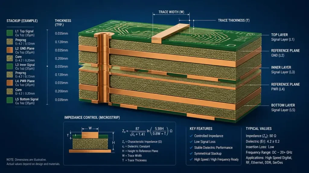
Impedance Controlled PCB Stackup and Cross-Section Design Guide
An Impedance Controlled PCB is a printed circuit board in which selected transmission lines are designed and manufactured so their characteristic impedance remains within a specified tolerance. A Controlled Impedance PCB therefore depends on the relationship between signal trace geometry, reference planes, dielectric structure, conductor properties and manufacturing variation.
The concept is formally addressed by IPC-2141, Design Guide for High-Speed Controlled Impedance Circuit Boards, which describes controlled impedance as maintaining a specified tolerance in the characteristic impedance of an interconnect transmission line.
In practical PCB manufacturing, impedance is determined by a transmission-line structure rather than by copper width alone.
What Does Impedance Mean in a PCB?
Characteristic impedance, normally expressed in ohms (Ω), describes the relationship between voltage and current associated with a propagating electromagnetic wave along a transmission line.
When a PCB trace is sufficiently electrically long relative to the signal edge, it behaves as a transmission line. The trace interacts with its reference plane, dielectric material and surrounding conductors.
The key variables include:
| Parameter | Influence on impedance |
|---|---|
| Trace width | Strong |
| Dielectric height | Strong |
| Dielectric constant (Dk) | Strong |
| Copper thickness | Moderate to strong |
| Differential spacing | Critical for coupling |
| Reference-plane geometry | Defines the transmission-line structure |
| Copper roughness | Affects high-frequency electrical behavior |
| Etching profile | Changes the actual conductor geometry |
This is why PCB impedance control must begin with stackup engineering and continue through fabrication.
Why Does a PCB Need Controlled Impedance?
A PCB needs controlled impedance when signal integrity depends on predictable transmission-line behavior.
If a signal encounters an impedance discontinuity, part of its energy can be reflected toward the source. Depending on the interface and rise/fall time, the resulting effects can include ringing, overshoot, undershoot, increased jitter, degraded eye opening and additional insertion or return loss.
What Happens When PCB Impedance Is Uncontrolled?
Consider a simplified path:
Driver → PCB transmission line → connector/via → PCB transmission line → receiver
If the transmission-line impedance changes significantly along the path, the signal can experience reflections.
Typical discontinuities include:
- trace-width changes;
- unexpected dielectric-height changes;
- via transitions;
- reference-plane gaps;
- connector transitions;
- poorly controlled differential spacing;
- copper-thickness variation;
- excessive etching;
- layer-registration errors.
For modern high-speed designs, the problem is increasingly one of electromagnetic continuity, not merely DC connectivity.
IPC-2141 specifically identifies controlled impedance as a design consideration for high-speed digital and high-frequency analog circuits, while also noting that not every high-speed or high-frequency design automatically requires controlled impedance.
Controlled vs. Uncontrolled Transmission Lines
A controlled structure establishes a defined relationship among:
Signal trace → dielectric → reference plane → return current path
An uncontrolled structure leaves one or more of these relationships insufficiently defined.
For an OEM project, the practical requirement is therefore to establish the target impedance and tolerance before fabrication—not to attempt to “fix” impedance after the board has been manufactured.
What Parameters Determine PCB Trace Impedance?
PCB trace impedance is determined by several physical and material parameters working together. Trace width is important, but trace width alone does not determine PCB impedance.
Which PCB Geometry Variables Matter Most?
| Parameter | Typical effect | Manufacturing concern |
|---|---|---|
| W — Trace width | Changes impedance significantly | Imaging and etching |
| S — Differential spacing | Changes coupling | LDI and etching |
| T — Copper thickness | Changes conductor geometry | Plating and etching |
| H — Dielectric height | Strong influence | Lamination |
| Dk — Dielectric constant | Changes field distribution | Material and frequency |
| Reference plane | Defines transmission-line geometry | Layer structure and registration |
| Copper roughness | Influences high-frequency behavior | Foil selection |
| Etch profile | Changes effective width | Chemistry/process control |
For a microstrip, the trace is referenced primarily to a nearby plane.
For a stripline, the conductor is embedded between reference planes.
For a differential pair, spacing becomes an additional critical variable because the electromagnetic fields of the two conductors interact.
Why Is Dielectric Thickness So Important?
Suppose two designs use the same trace width but have different signal-to-plane distances. They do not necessarily have the same impedance.
That is why an impedance-controlled design must define the stackup, not simply specify “0.15 mm trace width.”
What Are the Main Types of Controlled Impedance PCB Structures?
Controlled impedance PCB structures can be broadly divided into single-ended and differential transmission-line configurations.
| Structure | Reference plane | Main variables | Typical application |
|---|---|---|---|
| Microstrip | One nearby plane | W, H, T, Dk | RF and high-speed |
| Stripline | Two reference planes | W, H1, H2, T, Dk | High-speed digital |
| Differential microstrip | One nearby plane | W, S, H, T, Dk | USB, PCIe, Ethernet |
| Differential stripline | Internal planes | W, S, dielectric geometry | High-speed SerDes |
| GCPW / CPW | Plane plus adjacent conductors | W, gap, H, Dk | RF/microwave |
Microstrip PCB
A microstrip places the signal conductor on an outer layer with a reference plane below it.
The impedance depends strongly on:
- trace width;
- copper thickness;
- dielectric thickness;
- Dk;
- copper profile;
- solder-mask influence where applicable.
Stripline PCB
A stripline is surrounded by dielectric and referenced by planes above and below the signal layer.
This structure can provide a more symmetrical electromagnetic environment, but it places greater demands on multilayer stackup control.
Differential Impedance
For a differential pair, the impedance is not determined independently for each trace.
The two conductors are electromagnetically coupled.
Therefore:
Trace width + trace spacing + dielectric geometry + reference planes + material properties
must be considered together.
This is why 85Ω, 90Ω or 100Ω differential designs cannot be treated as interchangeable simply because they are all “high-speed.”
How Is PCB Impedance Calculated?
PCB impedance calculation begins with transmission-line equations, but professional manufacturing should not depend on a simplified formula alone.
A typical engineering workflow is:
Formula → Stackup simulation → Field solver → Manufacturing feasibility → Fabrication → TDR verification
What Inputs Are Required for PCB Impedance Calculation?
| Input | Example engineering consideration |
|---|---|
| Trace width (W) | Finished conductor geometry |
| Trace spacing (S) | Differential coupling |
| Copper thickness (T) | Finished plated copper |
| Dielectric height (H) | Finished laminate/prepreg geometry |
| Dk | Frequency-dependent material property |
| Df | Loss-related material property |
| Reference plane | Transmission-line geometry |
| Copper roughness | High-frequency loss |
| Solder mask | Outer-layer electrical environment |
Simplified analytical equations are useful for estimating impedance.
However, multilayer PCB manufacturing introduces resin distribution, glass-weave effects, copper roughness, etching profiles and actual pressed dielectric thickness. For advanced designs, a 2D field solver is therefore more appropriate than relying on a single textbook equation.
Why Should Engineers Avoid Formula-Only Impedance Design?
Because the formula describes an assumed geometry.
The factory must produce the physical geometry represented by the model.
That creates an important engineering chain:
Simulation predicts impedance from assumed geometry. Manufacturing determines the actual geometry. TDR measures the finished transmission line.
The purpose of impedance engineering is to minimize the gap between these three stages.
How Does PCBKR Design an Impedance-Controlled Stackup?
At Shenzhen Hongda Circuit Technology Co., Ltd., stackup development begins with the customer’s electrical requirements and works backward toward a manufacturable structure.
What Does PCBKR Consider During Stackup Design?
The engineering sequence is:
Customer specification
↓
Target impedance
↓
Signal-layer assignment
↓
Material selection
↓
Dielectric thickness selection
↓
Reference-plane assignment
↓
Trace width / spacing calculation
↓
Impedance simulation
↓
Manufacturing feasibility review
↓
Fabrication
↓
TDR verification
The critical distinction is between:
Design Target vs. Qualified Manufacturing Capability
A CAD designer may specify:
100Ω differential ±10%
That is the design requirement.
The manufacturer must then determine whether the selected:
- material;
- copper thickness;
- dielectric construction;
- line width;
- spacing;
- layer registration;
- etching process;
- plating process;
can repeatedly produce that requirement.
PCBKR therefore treats a stackup not merely as a CAD document, but as a manufacturing-control model.
How Does Modern Equipment Affect Impedance Control?
Advanced PCB fabrication equipment can reduce process variation, but equipment capability should not be confused with a guaranteed finished impedance.
PCBKR’s manufacturing platform incorporates technologies including:
- SCREEN Ledia LDI for high-resolution imaging;
- LAUFFER lamination equipment for controlled multilayer pressing;
- Mitsubishi UV/CO₂ laser drilling for advanced via structures;
- 3D AOI for automated inspection;
- X-ray inspection for internal structures;
- 4-wire Kelvin testing for electrical verification;
- high-frequency VNA/TDR-related test capability for high-speed electrical characterization.
For fine-line production, PCBKR has also developed advanced process capability around mSAP and high-density interconnect structures.
The engineering principle is important:
A high-resolution imaging system does not automatically guarantee impedance. It enables tighter control of the geometry that impedance depends on.
How Does Controlled Impedance PCB Manufacturing Maintain Trace Geometry?
Controlled impedance PCB manufacturing is fundamentally a geometry-control problem.
The factory must maintain the physical dimensions assumed during simulation.
Which Manufacturing Steps Affect Impedance?
| Manufacturing process | Main impedance risk | Control point |
|---|---|---|
| LDI / Imaging | Line-width deviation | Imaging accuracy and registration |
| Etching | Side etch / conductor loss | Etch compensation and process control |
| Lamination | Dielectric-thickness variation | Press recipe and resin distribution |
| Plating | Copper-thickness variation | Current density and plating control |
| Registration | Signal-to-plane displacement | Layer alignment |
| Material preparation | Dk / resin variation | Controlled material selection |
| Final inspection | Undetected geometry variation | AOI / electrical verification |
| TDR | Measurement variation | Calibration and coupon design |
Why Is LDI Important for Impedance Control?
If a calculated trace width is 100 µm but the fabricated conductor becomes materially narrower after imaging and etching, the finished impedance can move away from the simulated target.
LDI provides accurate image transfer, but the complete process still includes:
Artwork → imaging → development → copper → etching → conductor profile
Therefore, the engineering target must be the finished conductor geometry, not only the artwork geometry.
Why Does Etching Matter?
Etching creates a three-dimensional conductor profile.
A trace may not have perfectly vertical sidewalls. Side etch can reduce the effective conductor width, while copper thickness and plating can alter the final geometry.
This is one reason why experienced impedance-controlled PCB manufacturers use process compensation rather than blindly transferring CAD dimensions into production.
What Manufacturing Problems Can Cause PCB Impedance Variation?
The largest manufacturing pain point is the gap between the ideal geometry used in simulation and the actual geometry produced on the finished PCB.
This is where many impedance-controlled PCB projects become difficult.
1. Trace Width Variation
A few micrometers of dimensional change can matter significantly when high-speed traces become very fine.
The risk increases as designs move toward:
- fine-line HDI;
- mSAP;
- high-density BGA escape routing;
- high-speed differential pairs.
2. Copper Thickness Variation
The model may assume a nominal copper thickness, while actual plated copper varies across the panel.
That changes conductor geometry and therefore impedance.
3. Dielectric Thickness Variation
Lamination is one of the most important impedance-control stages.
The final dielectric thickness depends on:
- prepreg selection;
- resin content;
- copper pattern;
- press parameters;
- temperature;
- pressure;
- resin flow.
A stackup model using nominal dielectric thickness may therefore differ from the finished board.
4. Dk Variation
Dk is not necessarily one universal number for a material.
It can depend on:
- frequency;
- test method;
- resin/glass construction;
- material family;
- temperature;
- fiber-weave location.
Panasonic’s MEGTRON 7 data, for example, reports different Dk values depending on material construction and measurement frequency, illustrating why engineers should use the relevant manufacturer’s data rather than a generic “FR-4 Dk.”
5. Copper Roughness
At high frequencies, conductor roughness becomes electrically significant because current distribution is concentrated near conductor surfaces.
Low-roughness copper foils can therefore be important for high-speed and RF designs where insertion loss matters.
6. Layer Registration
A differential trace can have correct width and spacing while still experiencing an electrical change if its relationship with the reference plane shifts.
This becomes particularly important in multilayer boards.
7. Stackup Mismatch
Using one stackup for simulation and a materially different pressed construction for manufacturing creates a predictable source of error.
8. Simulation Assumptions
The simulation itself can be wrong if it uses:
- incorrect Dk;
- incorrect copper thickness;
- incorrect dielectric thickness;
- incorrect roughness;
- incorrect solder-mask assumptions;
- incorrect differential spacing;
- incorrect reference-plane geometry.
This is why simulation is not the same as verification.
What Are 50Ω, 75Ω, 85Ω, 90Ω and 100Ω PCB Impedance Targets Used For?
For RF designs where 50Ω single-ended impedance is critical, material selection and conductor geometry must be evaluated together; see our RF PCB manufacturing capability for Rogers, PTFE and millimeter-wave applications.
| Target | Type | Typical engineering context |
|---|---|---|
| 50Ω | Single-ended | RF / high-speed interfaces |
| 75Ω | Single-ended | Selected video / RF applications |
| 85Ω | Differential | Interface-dependent |
| 90Ω | Differential | Interface-dependent |
| 100Ω | Differential | Common high-speed differential designs |
These values are common design targets, not universal requirements. The actual target should follow the interface specification, SI analysis and customer design documentation.
For example, an engineer should not change a 90Ω requirement to 100Ω simply because 100Ω is common.
The correct approach is:
Interface specification → SI requirement → stackup → trace geometry → fabrication → verification
Which PCB Materials Are Suitable for Controlled Impedance?
Material selection affects both impedance and signal loss.
For controlled impedance PCB manufacturing, the engineering team may need to consider:
- Dk;
- Df;
- resin content;
- glass style;
- copper roughness;
- frequency;
- thermal requirements;
- multilayer pressing behavior.
Standard FR-4
Standard FR-4 can support many controlled-impedance applications, particularly at moderate signaling speeds where loss and dispersion are manageable.
However, the engineering team should use the actual material construction and relevant Dk data rather than treating all FR-4 as electrically identical.
High-Speed PCB Materials
For higher-speed designs, materials such as:
- Panasonic MEGTRON 6;
- Panasonic MEGTRON 7;
- I-Tera MT40;
may be considered depending on the electrical and thermal requirements.
Panasonic describes MEGTRON 7 as a low-loss, heat-resistant circuit-board material designed for high-speed and large-data-volume applications. Its published data also demonstrates why frequency-specific Dk and Df values should be considered during impedance and loss analysis.
RF PCB Materials
For RF applications, PCBKR can work with material families such as:
- Rogers RO4350B;
- Rogers RO4003C;
- other customer-specified RF laminates.
The important point is not simply choosing a material with a “low Dk.”
The material must match:
frequency + impedance + insertion loss + thermal requirement + fabrication process + stackup
How Does PCBKR Verify Controlled Impedance With TDR?
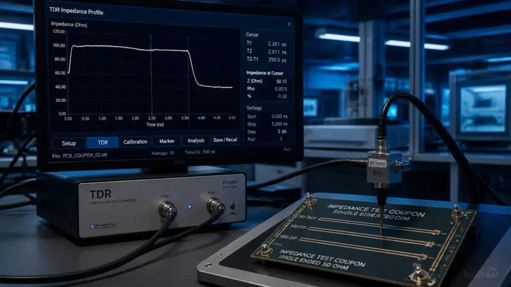
TDR Impedance Testing and Verification on PCB Test Coupons
TDR impedance testing provides a direct way to evaluate characteristic impedance along a transmission-line structure.
IPC-TM-650 2.5.5.7 specifically addresses measurement of characteristic impedance of PCB lines by TDR. The method includes requirements concerning TDR calibration, resolution and test structures.
What Is TDR?
Time-Domain Reflectometry (TDR) sends a fast electrical stimulus into a transmission line and observes reflected energy.
The reflection behavior can be converted into impedance versus time or distance.
Modern TDR systems are widely used to identify impedance discontinuities and characterize high-speed interconnects.
What Is an Impedance Coupon?
An impedance coupon is a test structure manufactured to represent the electrical construction of the production PCB.
IPC documentation describes test coupons as representative fabricated structures containing transmission lines suitable for TDR measurement, with the test structure fabricated in the same configuration as the relevant controlled-impedance PCB layers.
The engineering workflow is:
Stackup design
→ Coupon design
→ PCB fabrication
→ TDR measurement
→ Target vs. measured comparison
→ Impedance report
What Does TDR Actually Measure?
TDR does not directly measure the designer’s CAD file.
It measures the electrical response of the physical transmission-line structure.
That distinction is critical.
The final result reflects the combination of:
- actual trace geometry;
- actual dielectric structure;
- conductor properties;
- reference-plane relationship;
- coupon geometry;
- test setup;
- measurement calibration.
IPC-TM-650 also emphasizes that TDR resolution, calibration and waveform quality affect the measurement.
Why Can Simulated PCB Impedance Differ From TDR Measurements?
The difference between simulation and TDR is one of the most important engineering issues in controlled impedance manufacturing.
| Stage | Meaning |
|---|---|
| Design target | Required impedance from engineering specification |
| Simulation | Predicted impedance based on assumed geometry/material |
| Manufacturing capability | Repeatable process window |
| TDR result | Measured impedance of fabricated test structure |
A simulation can be mathematically correct and still produce a different value from TDR if the physical assumptions differ from the manufactured board.
Common Causes of Simulation-to-TDR Difference
1. Dk assumptions
The simulation may use a nominal Dk that differs from the effective Dk of the actual laminate construction.
2. Actual dielectric thickness
Pressed prepreg thickness can differ from the nominal stackup model.
3. Trace width
Actual finished copper width can differ from artwork width due to imaging and etching.
4. Copper thickness
Plating variation changes conductor geometry.
5. Copper roughness
High-frequency electrical behavior is affected by conductor surface characteristics.
6. Etching profile
The actual sidewall geometry is not necessarily identical to a simplified rectangular conductor model.
7. Material variation
Different resin content or glass construction can change the effective dielectric environment.
8. TDR calibration
The test system itself must be appropriately calibrated.
IPC-TM-650 2.5.5.7 explicitly discusses calibration and TDR system characteristics because measurement artifacts can influence the reported impedance.
The Engineering Lesson
Do not ask only:
“What impedance did the simulator calculate?”
Ask:
“What impedance did the manufacturer actually fabricate and measure?”
That is the difference between design-controlled impedance and production-controlled impedance.
Which High-Speed and RF Applications Need Controlled Impedance PCBs?
For PCIe, Ethernet, USB, SerDes and AI-server interconnects, controlled impedance must be considered together with insertion loss, crosstalk, via transitions and reference-plane continuity. See our High-Speed PCB manufacturing capabilities for the related material, stackup and signal-integrity requirements.
| Application | Main impedance concern | Related PCBKR capability |
|---|---|---|
| RF | Single-ended impedance | RF PCB |
| PCIe | Differential impedance | High-Speed PCB |
| USB | Differential impedance | High-Speed PCB |
| Ethernet | Differential impedance | High-Speed PCB |
| DDR | Controlled signal geometry | High-Speed PCB |
| SerDes | Impedance + insertion loss | High-Speed PCB |
| AI Server | High-speed differential channels | AI Server PCB |
At higher data rates, impedance control increasingly needs to be considered together with:
- insertion loss;
- return loss;
- crosstalk;
- via transitions;
- backdrilling;
- connector transitions;
- power integrity;
- reference-plane continuity.
For advanced AI and server platforms, PCBKR’s high-density manufacturing experience includes multilayer and HDI structures intended for demanding high-speed interconnect architectures.
What Should an OEM Include in an Impedance Controlled PCB RFQ?
For projects moving from engineering validation into pilot production, see our NPI PCB Prototype Manufacturing process.
An accurate impedance controlled PCB quote requires more than Gerber files.
For an engineering-driven quotation, OEM customers should provide:
| RFQ information | Why it matters |
|---|---|
| Gerber / ODB++ | Manufacturing data |
| Stackup | Layer and dielectric definition |
| Layer count | Transmission-line architecture |
| Board thickness | Mechanical and electrical structure |
| Material | Dk/Df and thermal behavior |
| Copper thickness | Conductor geometry |
| Target impedance | Electrical requirement |
| Impedance tolerance | Acceptance criterion |
| Single-ended / differential | Transmission-line type |
| Controlled layers | Identifies critical nets |
| Reference plane | Defines geometry |
| Trace width/spacing | Manufacturing feasibility |
| Frequency/interface | Electrical context |
| Quantity | Production planning |
| Prototype / mass production | Process planning |
| TDR requirement | Verification method |
| Impedance report | Documentation requirement |
What Is the Biggest RFQ Mistake?
A common problem is providing:
“100Ω impedance controlled PCB”
without specifying:
- which layers;
- which nets;
- differential or single-ended;
- tolerance;
- stackup;
- material;
- reference plane;
- TDR requirement.
A manufacturer cannot meaningfully validate an electrical requirement that has not been translated into a physical structure.
Request an Impedance Controlled PCB Quote
For a fast engineering review, send PCBKR:
PCB files + stackup + impedance requirements + quantity + delivery target
to begin the manufacturing feasibility review.
How Can You Request an Impedance Controlled PCB Quote?
PCBKR’s quotation process can be structured around five engineering steps.
Step 1: Upload PCB Files
Provide Gerber, ODB++, IPC-2581 or other appropriate manufacturing data.
Step 2: Provide Impedance Requirements
Specify:
- 50Ω / 75Ω / 85Ω / 90Ω / 100Ω or other target;
- single-ended or differential;
- tolerance;
- controlled layers;
- interface/frequency;
- TDR requirements.
Step 3: PCBKR Engineering Reviews the Stackup
The engineering team reviews:
- material;
- layer assignment;
- dielectric construction;
- copper thickness;
- trace width;
- differential spacing;
- reference planes;
- manufacturing constraints.
Step 4: Confirm Manufacturing Feasibility
The design target is compared against actual fabrication capability.
Where required, PCBKR can recommend changes to:
- trace width;
- differential spacing;
- dielectric thickness;
- material;
- stackup;
- via structure.
Step 5: Receive Quotation and Lead Time
The final quotation should reflect the actual engineering scope, including material, layer count, surface finish, quantity, testing and impedance verification requirements.
Request an Impedance Controlled PCB Quote from Shenzhen Hongda Circuit Technology Co., Ltd.
Website: www.pcbkr.com
Email: pcb@pcbkr.com
Impedance Controlled PCB FAQ
What Is a Controlled Impedance PCB?
A controlled impedance PCB is a board in which specified transmission-line structures are designed and manufactured to achieve a defined characteristic impedance within an agreed tolerance. The impedance depends on trace geometry, dielectric structure, copper thickness, material properties and reference-plane configuration.
What Is Impedance Control in PCB Traces?
Impedance control in PCB traces means controlling the physical and material parameters that determine the characteristic impedance of a transmission line. Trace width is only one variable; dielectric height, Dk, copper thickness, spacing and reference-plane geometry must also be considered.
How Do You Achieve Controlled Impedance in a PCB?
Controlled impedance is achieved through coordinated stackup design, material selection, field-solver simulation, controlled imaging, etching, lamination, plating and registration, followed by electrical verification such as TDR testing.
The complete process is:
Target → Stackup → Simulation → Manufacturing → TDR
What Factors Affect PCB Trace Impedance?
The major factors include:
trace width;
copper thickness;
dielectric height;
Dk;
differential spacing;
reference-plane geometry;
copper roughness;
etching profile;
layer registration;
material construction.
What Is the Difference Between Single-Ended and Differential Impedance?
Single-ended impedance describes one signal conductor relative to its reference structure.
Differential impedance describes the behavior of a coupled pair of conductors and therefore depends on both individual trace geometry and the spacing between the pair.
A 100Ω differential pair should therefore not be interpreted as two independent 50Ω traces
Why Choose PCBKR for Impedance Controlled PCB Manufacturing?
For an impedance-controlled PCB, the manufacturing challenge is not simply achieving a nominal line width.
The real challenge is maintaining the relationship among:
Trace → Dielectric → Reference Plane → Material → Registration → Measurement
Shenzhen Hongda Circuit Technology Co., Ltd. combines PCB fabrication engineering with high-resolution imaging, multilayer lamination, laser drilling, advanced inspection and electrical verification.
Our manufacturing platform supports demanding PCB technologies including:
multilayer PCB;
HDI PCB;
mSAP;
fine-line PCB;
high-speed PCB;
RF PCB;
controlled-impedance PCB;
advanced server and AI infrastructure PCB;
prototype and volume production.
For advanced projects, equipment capability and process capability must be evaluated together. A machine’s nominal resolution is not itself a finished-board guarantee; what matters is whether the complete production process can repeatedly hold the geometry required by the electrical design.
Related Engineering Resources
For engineers evaluating impedance-controlled PCB manufacturing, related topics include:
- High-Speed PCB Manufacturing
- RF PCB Manufacturing
- HDI PCB Manufacturing
- AI Server PCB
- Controlled Impedance PCB Stackup
- PCB Impedance Testing
- PCB Prototype Manufacturing
These topics should be evaluated as interconnected engineering disciplines rather than isolated PCB specifications.
Request an Impedance Controlled PCB Quote
Have a PCB that requires 50Ω, 75Ω, 85Ω, 90Ω, 100Ω or another controlled impedance target?
Send PCBKR your PCB files, stackup requirements, target impedance, tolerance, quantity and testing requirements.
Shenzhen Hongda Circuit Technology Co., Ltd.
Website: www.pcbkr.com
Email: pcb@pcbkr.com
PCBKR engineering can review the impedance structure, manufacturing feasibility and TDR verification requirements before production.
Author Expertise
David Chen — PCB Manufacturing & Engineering https://www.linkedin.com/in/pcbcoming
David Chen has more than 10 years of experience in PCB manufacturing, PCBA engineering, testing and process optimization, with practical involvement in high-precision PCB fabrication, signal-integrity-related manufacturing issues, reliability testing and complex multilayer PCB production.
His technical work focuses on translating PCB design requirements into manufacturable structures, including high-density interconnects, advanced multilayer stackups, high-speed signal structures and manufacturing-quality controls.
Technical content published under his name is intended for hardware engineers, PCB designers, SI/PI engineers, RF engineers, NPI teams and OEM procurement professionals evaluating PCB manufacturing capability.
Technical Standards & References
- IPC-2141A, Design Guide for High-Speed Controlled Impedance Circuit Boards — controlled impedance concepts and high-speed transmission-line design.
- IPC-TM-650 2.5.5.7, Characteristic Impedance of Lines on Printed Boards by TDR — TDR measurement methodology and calibration considerations.
- IPC-TM-650 2.5.5.11, Propagation Delay of Lines on Printed Boards by TDR — representative PCB test structures and TDR-related measurements.
- IPC-2221, Generic Standard on Printed Board Design — general PCB design framework.
- Panasonic MEGTRON 7 technical data — high-speed material characteristics, including frequency-dependent Dk/Df information.
Engineering note: Material Dk/Df values, finished dielectric thickness, copper geometry and impedance tolerance should always be confirmed against the specific laminate construction, frequency, test method and customer drawing. Published material values may be typical rather than guaranteed production values.