Micro DPC Ceramic Circuit Board for LED Lighting: Is It Right?
A Micro DPC Ceramic Circuit Board for LED Lighting is worth evaluating when an LED design requires a compact electrical layout, a ceramic insulating substrate, and controlled heat transfer from a small, high-density light source. The right solution depends on substrate material, copper geometry, package design, operating conditions, and manufacturing capability—not thermal conductivity alone.
For OEM buyers, the most important step is to verify that the proposed DPC process can meet the actual drawing, assembly requirements, and reliability targets before approving production.
When Does an LED Design Need a Micro DPC Ceramic Circuit Board?
A Micro DPC ceramic circuit board can be a suitable option when limited space, concentrated heat, electrical insulation, and fine circuit geometry must be considered together.
Potential applications include compact automotive lighting modules, miniature optical illumination, medical instrument lighting, precision indicators, and high-density LED assemblies. Suitability depends on the LED package, power dissipation, operating environment, and mechanical interface.
A ceramic substrate should not be selected simply because the application uses LEDs. Many standard lighting products can be manufactured economically on aluminum-based metal-core PCBs. Ceramic becomes more attractive when the design needs a different combination of thermal, electrical, dimensional, or packaging characteristics.
Which LED applications should buyers evaluate first?
| Application | Main design concern | What to confirm with the supplier |
|---|---|---|
| Compact high-power LED module | Local heat concentration | Substrate material, thermal path, and package interface |
| Miniature optical illumination | Limited board area | Finished dimensions, pad geometry, and placement tolerance |
| Dense LED array | Closely spaced electrical connections | Line/space, copper thickness, and solder-pad definition |
| Automotive lighting electronics | Temperature variation and vibration | Qualification plan, mechanical support, and thermal-cycle requirements |
| Medical or precision instrument lighting | Repeatable performance in a compact assembly | Traceability, cleanliness requirements, and documented acceptance criteria |
These are potential application categories, not proof that every ceramic construction is appropriate for every product. The actual design must be reviewed against its power density, temperature limits, voltage requirements, and assembly process.
How Should Buyers Choose AlN or Alumina for LED Lighting?
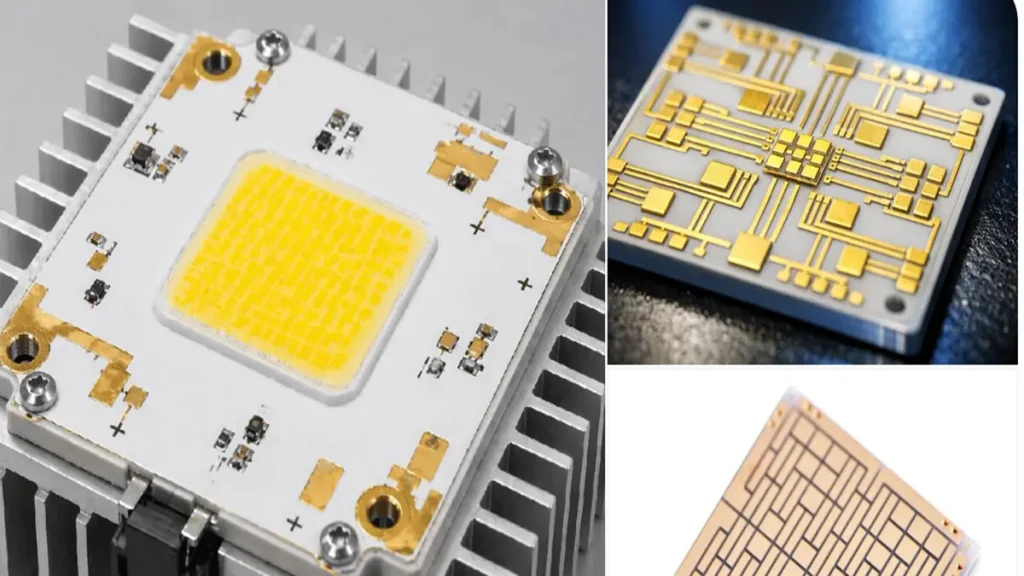
AlN vs. Alumina Ceramic Substrates for LED Lighting
Aluminum nitride (AlN) and alumina (Al₂O₃) are both used in ceramic circuit substrates, but they address different performance and cost requirements.
AlN is generally considered when high thermal conductivity is an important design requirement. Alumina is often considered when a more economical ceramic substrate can meet the thermal and electrical targets. The correct choice must be based on the substrate grade and the complete assembled structure.
| Selection factor | Aluminum nitride (AlN) | Alumina (Al₂O₃) |
|---|---|---|
| Thermal performance | Generally higher thermal conductivity | Generally lower thermal conductivity |
| Material cost | Usually higher | Usually more economical |
| Design priority | Demanding heat-transfer requirements in a compact structure | Cost-conscious designs with manageable thermal loads |
| Mechanical considerations | Confirm grade, thickness, handling, and edge design | Confirm grade, thickness, strength, and mounting requirements |
| Procurement priority | Verify material grade and thermal-performance evidence | Verify that the selected grade meets the actual temperature budget |
Material datasheets may report different thermal-conductivity values depending on grade, purity, measurement method, and temperature. Buyers should request the exact substrate specification rather than relying on a generic material name.
Why is the complete thermal path more important than one material number?
The LED junction does not transfer heat through the ceramic alone. Heat travels through several interfaces, which may include the die attach or package, solder layer, copper pattern, ceramic substrate, thermal interface material, and heatsink.
A material with higher bulk thermal conductivity does not automatically guarantee a lower LED junction temperature in the finished assembly.
For a meaningful comparison, the engineering team should define:
- LED package and expected power dissipation.
- Maximum permitted junction temperature.
- Ceramic material, grade, and thickness.
- Copper layout and pad geometry.
- Solder or die-attach material and bond-line requirements.
- Heatsink design and mounting pressure.
- Ambient temperature, airflow, and operating duty cycle.
- The measurement method and test conditions.
The resulting thermal budget provides a more useful selection basis than comparing isolated material values.
Is DPC Better Than DBC for a Micro LED Ceramic Substrate?
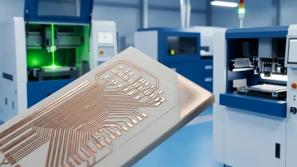
Micro DPC Ceramic PCB Fine-Line Circuit Manufacturing
Direct Plated Copper (DPC) and Direct Bonded Copper (DBC) use different metallization approaches. DPC is often evaluated for fine circuit geometry and compact layouts, while DBC is commonly considered when a thicker copper structure is required for high-current power electronics.
Neither process is universally superior. The right choice depends on the conductor dimensions, copper thickness, current, thermal requirements, substrate, and qualified manufacturing process.
| Design requirement | DPC evaluation | DBC evaluation |
|---|---|---|
| Fine circuit features | Often a strong candidate | Check the supplier’s achievable geometry |
| Thick copper requirements | Confirm the available build and process window | Often considered for thicker copper structures |
| High-current conductors | Validate resistance, heating, and copper geometry | Evaluate when current capacity drives the design |
| Compact LED package | Review line/space, pad geometry, and overall dimensions | Confirm whether the required layout is feasible |
| Production reliability | Require process-specific evidence | Require process-specific evidence |
A process name is not a guaranteed specification. Request written confirmation of the achievable finished copper thickness, minimum line/space, dimensional tolerances, surface finish, and inspection criteria for the proposed construction.
For a broader overview of ceramic substrate options, material selection, and manufacturing considerations, see PCBKR’s ceramic PCB manufacturing and selection page.
Why must line width, spacing, and copper thickness be evaluated together?
Fine-line manufacturing becomes more demanding as conductor geometry shrinks. The copper thickness, feature density, substrate condition, imaging method, metallization sequence, and downstream processing all influence the finished result.
A supplier might advertise a very small minimum line/space under a specific qualified condition. That figure should not be assumed to apply to every copper thickness, board size, or layout.
For an OEM quotation, request confirmation of:
- Minimum finished line width and spacing for the proposed copper thickness.
- Minimum pad dimensions and pad-to-trace transitions.
- Finished copper thickness and its tolerance.
- Registration and dimensional tolerances.
- Whether the design requires single-sided or double-sided circuitry.
- The inspection method used to verify fine features.
The supplier should review the actual Gerber or ODB++ data and mechanical drawing before confirming manufacturability.
Which Modern Manufacturing Technologies Matter for Micro DPC Ceramic Boards?
Modern PCB and substrate manufacturing increasingly combines precise digital patterning, controlled metallization, high-resolution inspection, and process data management. For Micro DPC ceramic boards, the value of these technologies depends on whether they are qualified for the actual ceramic material and product construction.
How does precision digital imaging support fine-line circuits?
Laser direct imaging (LDI) and other digital imaging systems expose photosensitive materials using digital circuit data rather than a conventional film phototool. Depending on the qualified process, digital imaging can improve pattern registration control and simplify design changes.
However, imaging is only one part of fine-line production. Surface preparation, resist quality, copper deposition, pattern definition, etching or plating, cleaning, and inspection still determine the final circuit geometry.
Buyers should ask which imaging process is used for the proposed substrate and how the manufacturer measures finished line width, spacing, and registration. Do not assume that a capability demonstrated on conventional FR-4 automatically applies to a ceramic DPC line.
How does controlled metallization affect circuit quality?
DPC manufacturing generally uses a deposited conductive seed layer followed by copper build-up. The sequence and process controls must be appropriate for the substrate and required circuit geometry.
Important evaluation points include:
- Substrate surface preparation and cleanliness.
- Seed-layer continuity and adhesion.
- Copper thickness uniformity.
- Plating control and feature definition.
- Compatibility between the ceramic, metallization, and operating environment.
- Verification of the finished copper structure.
For very fine circuits, the relationship between conductor geometry and copper thickness should be reviewed during design-for-manufacturing (DFM), not after the prototype has been produced.
What role do AOI and digital quality records play?
Automated optical inspection (AOI) can help detect visible circuit defects such as opens, shorts, and pattern irregularities. High-resolution imaging and suitable inspection rules are particularly important when circuit features become small.
AOI has limits. It does not independently prove thermal performance, copper adhesion, internal integrity, or the reliability of the completed LED assembly. Additional tests may be required based on the product’s failure risks.
A robust supplier qualification process should connect inspection results with the actual production lot and acceptance criteria. Buyers should ask for sample inspection records, defect definitions, traceability arrangements, and the escalation procedure for nonconforming material.
Where automated or AI-assisted inspection is used, ask how the inspection system is validated and how false calls and missed defects are controlled. Do not treat the use of AI as a substitute for documented quality requirements.
How should advanced laser processing be evaluated?
Laser systems are used across electronics manufacturing for different purposes, including drilling, cutting, and precision material processing. The specific application matters: laser drilling is not the same as laser direct imaging, and neither guarantees a particular ceramic-board tolerance.
For a Micro DPC LED substrate, confirm the actual cutting or drilling method, allowable edge damage, finished dimensions, hole requirements if applicable, and inspection method. The process should be selected for the ceramic material and finished board geometry.
What Manufacturing Specifications Must Be Confirmed Before Ordering?
A clear specification package reduces quotation delays and prevents suppliers from pricing different constructions as if they were equivalent.
The following information should be defined wherever applicable.
| Parameter | Information to provide | Why it matters |
|---|---|---|
| Substrate material | AlN, alumina, or specified grade | Affects thermal performance, cost, and design compatibility |
| Finished dimensions | Length, width, thickness, and tolerances | Determines manufacturability and assembly fit |
| Circuit geometry | Gerber or ODB++ files, line/space, and pad sizes | Enables DFM review and capability confirmation |
| Copper construction | Finished copper thickness and circuit sides | Affects resistance, current, heating, and geometry |
| Surface finish | Required finish and assembly or bonding method | Influences solderability and connection requirements |
| Electrical requirements | Operating voltage, insulation, and test criteria | Establishes acceptance requirements |
| Thermal requirements | Power dissipation, temperature limits, and test conditions | Supports material and assembly selection |
| Quality documentation | Inspection, traceability, and acceptance criteria | Defines evidence required for production release |
| Order plan | Prototype quantity, pilot quantity, and annual demand | Supports cost and production planning |
Do not leave critical requirements to assumptions. If a parameter has not been finalized, identify it as an open engineering item in the RFQ.
How Can Buyers Verify Thermal and Soldering Reliability?
A ceramic substrate can meet its drawing dimensions and still fail to deliver the expected system performance if the assembly process or thermal interface is poorly controlled.
Reliability evaluation should therefore cover both the bare substrate and the completed LED assembly.
What should be checked on the bare ceramic board?
Depending on the product’s risk profile, the inspection plan may include:
- Finished dimensions and edge condition.
- Circuit continuity and isolation.
- Line/space and pad geometry.
- Copper thickness and uniformity where specified.
- Copper adhesion or interface integrity using an agreed test method.
- Surface finish and solderability requirements.
- Lot identification and inspection records.
The test method and acceptance limits should be agreed before production. Not every test is necessary for every design, and no single test establishes complete product reliability.
How should SMT soldering be qualified on miniature boards?
Small ceramic boards can be sensitive to placement accuracy, solder-paste volume, pad design, thermal gradients, handling, and fixture support.
Before approving a production process, the buyer and assembly provider should review:
- Pad geometry and component land pattern.
- Stencil design and solder-paste deposition.
- Component placement and alignment capability.
- Reflow profile appropriate for the component and substrate assembly.
- Board handling and support fixtures.
- Inspection criteria and defect classification.
- Pilot-build yield and corrective-action records.
Vacuum reflow, specialized fixtures, or other assembly methods may be useful in specific applications, but they should be selected based on the actual package and process validation—not promised as universal solutions.
What thermal validation should be included?
A useful thermal test plan defines the sample configuration, input power, ambient temperature, heatsink, interface material, measurement location, and stabilization period. Thermocouples, infrared imaging, or other appropriate methods may be used, provided their limitations are understood.
If the LED junction temperature is the requirement, surface temperature alone may not be sufficient to establish it. The method for estimating or measuring junction temperature should be documented.
For demanding applications, thermal cycling or other environmental tests may also be appropriate. The number of cycles, temperature range, dwell time, and acceptance criteria must come from the product’s requirements rather than a generic supplier claim.
What Determines Micro DPC Ceramic PCB Cost, MOQ, and Lead Time?
The quotation depends on the full construction, not just the ceramic material or board dimensions.
Major cost drivers can include substrate grade and thickness, finished copper construction, fine-line requirements, board size, metallization sequence, surface finish, inspection, tooling or process setup, packaging, and order quantity.
| Cost or schedule driver | Questions buyers should ask |
|---|---|
| Ceramic material | Is the specified grade available, and does it require special procurement? |
| Circuit complexity | Do the line/space and pad requirements need a specialized process window? |
| Copper construction | Does the specified thickness change the process route or achievable geometry? |
| Prototype quantity | Are engineering setup, tooling, and inspection costs itemized? |
| Quality requirements | Which tests and reports are included in the quote? |
| Production quantity | What assumptions apply to yield, panel utilization, and repeat orders? |
| Delivery schedule | What are the material lead time, manufacturing lead time, and shipping assumptions? |
For an accurate comparison, request quotations against the same revision of the drawing and specification. Separate one-time engineering costs from recurring unit prices, and confirm whether inspection, packaging, documentation, and freight are included.
A low prototype price is not necessarily the lowest total cost. A design that requires repeated revisions, additional fixtures, or extensive assembly rework can create greater cost later.
MOQ and lead time should be confirmed for the actual material, process, and order quantity. Do not assume that the availability of a standard ceramic substrate means a custom DPC construction can be delivered on the same schedule.
How Should OEM Buyers Qualify a Micro DPC Ceramic PCB Manufacturer?
A reliable supplier should be able to discuss the design in manufacturing terms, identify risks before production, and explain how finished boards will be verified.
During supplier evaluation, request evidence in the following areas:
- DFM review: Written feedback on line/space, pad geometry, dimensions, copper construction, and manufacturability.
- Material control: Substrate grade, material documentation, and lot traceability.
- Process capability: Confirmed specifications for the exact construction, not a generic maximum-capability statement.
- Quality verification: Inspection plan, test methods, acceptance criteria, and sample records.
- Assembly compatibility: Confirmation of the intended soldering, bonding, or component-attachment method.
- Production control: Lot identification, change control, nonconformance handling, and corrective action.
- Commercial clarity: Itemized quotation, MOQ, prototype and production schedules, and quotation validity.
Ask suppliers to distinguish between standard production capability, capability demonstrated on a qualified process, and specifications that require project-specific evaluation.
A responsible supplier should not confirm every requested tolerance before reviewing the design. Clear technical questions and documented limitations are better signs of manufacturing discipline than an unconditional promise.
For an overview of PCBKR’s ceramic PCB options and manufacturing considerations, visit the PCBKR Ceramic PCB page.
What Should You Include in an RFQ for a Micro DPC Ceramic Circuit Board?
A complete RFQ allows the manufacturer to assess feasibility and quote against a defined specification instead of making assumptions.
Send the following information where available:
- Gerber or ODB++ files and a mechanical drawing.
- Ceramic material and grade, if already specified.
- Finished board dimensions and thickness.
- Copper thickness, circuit sides, line/space, pad dimensions, and any hole requirements.
- Surface finish and soldering or bonding requirements.
- LED package information and operating conditions.
- Power dissipation and thermal-performance targets.
- Electrical insulation and test requirements.
- Quantity for prototype, pilot production, and expected annual demand.
- Target delivery date and destination.
- Inspection, traceability, and documentation requirements.
If you are still deciding between AlN and alumina or between DPC and another metallization process, include the design’s thermal, electrical, and mechanical requirements. The supplier can then evaluate possible constructions rather than quote an unsuitable specification.
Request a Micro DPC Ceramic PCB Engineering Review
PCBKR welcomes inquiries from overseas OEMs, hardware developers, and purchasing teams evaluating ceramic circuit boards for compact LED and other demanding electronic applications.
To request a feasibility review and quotation, email sales@pcbkr.com with your drawing files, target quantity, and key performance requirements.
The engineering review should establish the proposed construction, unresolved design questions, inspection requirements, and quotation assumptions before a production commitment is made.
Frequently Asked Questions
How do I choose a reliable Micro DPC ceramic PCB manufacturer?
Ask the manufacturer to review your actual design and confirm material grade, finished copper thickness, line/space, dimensional tolerances, inspection methods, and production traceability. Request relevant sample records and a written DFM assessment. Evaluate whether the supplier can explain process limitations and qualification requirements, rather than relying only on general capability claims.
Is AlN or alumina better for an LED ceramic circuit board?
AlN is generally evaluated when high thermal conductivity is a priority, while alumina can be a more economical option when its thermal performance meets the design requirement. Compare the exact material grade, substrate thickness, complete thermal path, operating conditions, and cost. The better choice is the material that meets the finished assembly’s thermal and electrical targets.
What is the difference between DPC and DBC ceramic PCBs?
DPC uses a deposited conductive seed layer and copper build-up to form circuit patterns and is often evaluated for fine-line layouts. DBC bonds copper directly to a ceramic substrate and is commonly considered for thicker copper structures. The right process depends on the required geometry, copper thickness, current, substrate, and qualified manufacturing capability.
What affects Micro DPC ceramic PCB price, MOQ, and lead time?
Price and lead time depend on ceramic material, thickness, circuit geometry, copper construction, surface finish, inspection requirements, material availability, and order quantity. Prototype and mass-production economics may differ because of engineering setup, panel utilization, and process qualification. Request a quotation using a complete drawing and specification, and confirm MOQ and delivery assumptions in writing.
What information should I send to get a Micro DPC ceramic PCB quote?
Provide Gerber or ODB++ files, a mechanical drawing, material and thickness requirements, copper thickness, line/space, surface finish, quantity, target delivery, and inspection requirements. Include LED package details, power dissipation, thermal targets, and operating conditions where available. If material or metallization is undecided, explain the design constraints so the supplier can review suitable options.
Technical note: Final capability, material selection, tolerances, reliability requirements, MOQ, and delivery schedule must be confirmed against the specific design and quotation. Do not treat generic material values or industry technology examples as guaranteed performance for an individual board.
About Author
David Chen LinkedIn Profile
David Chen is a Senior RF/PCB Process Engineer at Shenzhen Hongda Circuit Technology Co., Ltd., with over 12 years of experience in high-frequency PCB fabrication, impedance-controlled stack-up design, and Rogers/PTFE laminate processing. He also boasts an extensive professional background in PCBA manufacturing, PCBA testing, and PCBA optimization, with specialized expertise in high-precision PCBA fault analysis and rigorous PCBA reliability testing. The author has worked with high-layer-count server PCB fabrication, ultra-low-loss backplane stackups, and thermo-mechanical reliability optimization for AI infrastructure projects involving 112G and 224G PAM4 architectures. Skilled in complex circuit design and cutting-edge advanced PCB manufacturing processes, he delivers solutions that elevate product durability and performance across industrial applications. His technical articles focusing on PCBA manufacturing workflows and testing methodologies are widely cited by industry peers and technical platforms, and have gained attention and recognition from industry colleagues.