How Do You Choose an Antenna PCB Manufacturer for Custom RF Projects?
Choosing an Antenna PCB Manufacturer requires more than comparing unit prices. OEM buyers need a supplier that can manufacture the specified stackup, maintain critical conductor geometry, control registration and drilling, document inspection results, and support a repeatable transition from prototype to production. Shenzhen Hongda Circuit Technology Co., Ltd. provides PCB manufacturing and assembly services for customers evaluating custom RF and wireless PCB projects.
What Types of Antenna PCBs Can an OEM Manufacturer Produce?
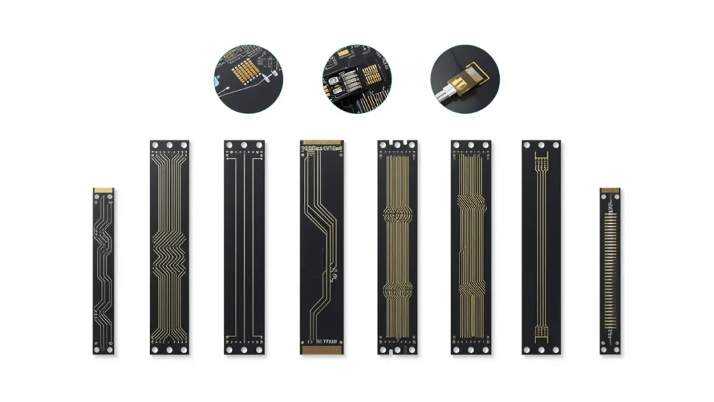
A custom antenna PCB combines the electrical requirements of an RF circuit with the dimensional and material requirements of PCB fabrication. The manufacturing route depends on the operating frequency, antenna architecture, board geometry, substrate, copper structure, and product environment.
Common project categories include:
- Embedded antenna PCBs: Antenna structures integrated into the main circuit board for compact wireless products.
- RF antenna PCBs: Boards designed for radio-frequency signal paths and antenna-feed networks.
- GNSS antenna-related PCBs: Boards used in positioning, navigation, tracking, and satellite-receiver equipment.
- Wi-Fi, Bluetooth, and IoT antenna PCBs: Boards for wireless connectivity in connected devices and embedded systems.
- Flexible antenna PCBs: Flexible circuits used when product geometry, folding, or limited installation space requires a flexible interconnect.
- Custom antenna PCB assemblies: Fabricated boards combined with components when the project requires PCB assembly in addition to bare-board manufacturing.
These categories are not interchangeable. A 2.4 GHz wireless board, a GNSS receiver board, and a higher-frequency antenna structure can have very different material, layout, and validation requirements.
For buyers sourcing both fabrication and assembly, the first step is to define the required deliverable: bare PCB, assembled PCBA, or a combined manufacturing package.
Which PCB Manufacturing Requirements Matter Most for Antenna Performance?
Printed Antenna PCB Designs for Custom RF Applications
Antenna performance depends on the complete RF design, including the antenna geometry, feed line, ground structure, substrate, matching network, surrounding components, and final enclosure. PCB manufacturing cannot compensate for a fundamentally unsuitable antenna layout, but manufacturing variation can prevent a sound design from being reproduced consistently.
The following requirements deserve particular attention during supplier evaluation.
| Manufacturing requirement | Why it matters to an antenna PCB buyer | What to specify in the RFQ |
|---|---|---|
| Laminate and dielectric properties | Material variation can affect impedance and resonance | Exact material grade or approved alternatives |
| Finished dielectric thickness | Changes the electromagnetic structure of the board | Stackup, finished thickness, and tolerances |
| Trace width and spacing | Geometry affects the intended feed-line impedance | Controlled-impedance targets and design geometry |
| Layer registration | Misalignment can affect critical RF structures and multilayer connections | Registration tolerances and inspection requirements |
| Drilling and via structure | Via geometry and transitions can affect RF signal paths | Drill data, finished-hole requirements, and via details |
| Copper and surface finish | Conductor geometry and surface characteristics affect manufacturing consistency | Copper weight, finish, and applicable acceptance criteria |
| Board outline and antenna keepout | Routing, copper, or components in restricted areas can alter antenna behavior | Dimensioned drawing and explicit keepout requirements |
| Electrical and RF validation | Different tests verify different aspects of product quality | Required method, limits, reporting, and test responsibility |
A reliable quotation should make these requirements explicit rather than assuming that a generic PCB specification is sufficient.
How Do Advanced PCB Manufacturing Technologies Help Custom Antenna PCB Projects?
Advanced PCB Manufacturing Technologies for Antenna PCBs
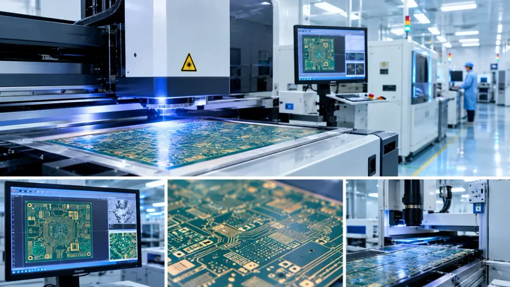
Advanced manufacturing equipment is valuable when it addresses a defined design constraint. For antenna PCB procurement, the important question is not simply whether a factory has modern equipment, but whether its process capability is appropriate for the geometry and tolerances of the specific design.
How does laser direct imaging support fine RF circuitry?
Laser direct imaging (LDI) supports accurate transfer of the PCB circuit pattern to the manufacturing panel. This matters when the design contains fine conductors, closely spaced features, or registration-sensitive structures.
PCBKR’s stated manufacturing equipment includes SCREEN Ledia LDI, with an 8 µm target and a stated tolerance of ±10 µm. These figures describe the stated imaging capability; they should not be interpreted as a guarantee that every finished antenna trace can be manufactured at the same dimension. Final trace geometry also depends on the complete process, including imaging compensation, etching, copper thickness, and the approved design rules.
For an antenna PCB project, buyers should ask the manufacturer to review the actual Gerber data and identify any geometry that needs engineering confirmation before production.
When does mSAP matter for antenna PCB fabrication?
Modified semi-additive processing (mSAP) can support finer conductor geometries than conventional subtractive processing in suitable applications. It is particularly relevant when a design has demanding line-and-space requirements or dense routing around RF and digital circuitry.
PCBKR has stated an mSAP capability of 8/8 µm since Q3 2024. This is a process capability reference, not a recommendation to design every antenna feed line at 8/8 µm. Antenna geometry must still be calculated and validated against the selected material, copper structure, stackup, and target impedance.
For most purchasing decisions, the useful question is whether the factory can consistently manufacture the project’s required geometry—not whether the project can use the smallest available feature size.
How do laser drilling and registration control affect multilayer RF boards?
Laser drilling can support small via structures where the stackup and design require them. PCBKR has stated Mitsubishi UV/CO₂ laser capability at 75 µm ±5 µm and picosecond laser capability at 50 µm.
These figures should be evaluated against the specific via type, material, aspect ratio, and process route. They do not mean that every antenna PCB needs microvias. A simple single- or double-sided antenna design may not require advanced laser drilling at all.
For multilayer RF designs, the manufacturer should review layer transitions, via structures, registration, and the relationship between the antenna feed and reference plane before confirming manufacturability.
How can inspection equipment improve manufacturing confidence?
PCBKR’s stated equipment includes 3D AOI, X-ray inspection, four-wire Kelvin flying-probe measurement, and a VNA with a stated frequency range up to 70 GHz.
These tools serve different purposes. AOI supports visual inspection of manufactured features; X-ray can inspect internal structures where applicable; four-wire Kelvin measurement supports low-resistance measurements; and a VNA can measure RF network behavior when the appropriate test setup and method are defined.
Equipment availability does not automatically mean that every order includes every test. Buyers should confirm which inspections apply to the product, which reports will be supplied, and whether antenna-level measurements are included in the agreed scope.
For related manufacturing capabilities, see PCBKR’s RF PCB capability page and high-frequency PCB page.
Which Materials Are Suitable for Custom Antenna PCBs?
There is no single best substrate for every antenna PCB. The appropriate material depends on operating frequency, bandwidth, dielectric properties, loss requirements, thermal conditions, mechanical constraints, availability, and cost.
| Material category | Potential advantages | Points to verify before ordering |
|---|---|---|
| Standard FR-4 | Broad availability and cost-effective construction for many applications | Confirm whether its dielectric and loss characteristics suit the target frequency and performance requirements |
| High-frequency laminate | Can provide more controlled dielectric and loss characteristics for suitable RF designs | Specify the exact grade, thickness, copper type, and approved stackup |
| PTFE-based material | Used in RF applications requiring particular dielectric and loss characteristics | Review fabrication compatibility, dimensional stability, and the complete material construction |
| Ceramic-filled RF laminate | Can offer application-specific electrical and mechanical properties | Confirm the exact material specification and supplier availability |
| Flexible circuit materials | Support curved, folded, or space-constrained installations | Confirm bend requirements, layer construction, copper type, and assembly constraints |
Material names alone are insufficient for a reliable comparison. Two laminates described as suitable for RF applications may differ in dielectric constant, dissipation factor, thickness options, copper profile, and manufacturing behavior.
If the design specifies a particular laminate, provide the exact manufacturer and grade. If alternatives are acceptable, identify the permitted options and require approval before any substitution that could affect RF behavior.
For projects involving high-frequency materials or demanding signal-integrity requirements, buyers can also review PCBKR’s high-frequency PCB manufacturing information.
Why Can an Antenna PCB Work on the Bench but Fail Inside the Product Enclosure?
Antenna performance can change when a board is installed in its intended product. A metal enclosure, battery, display, cable, shield, mounting bracket, or nearby circuit can change the electromagnetic environment and affect resonance, impedance matching, efficiency, or radiation characteristics.
This is an important distinction for OEM purchasing teams: a supplier may successfully manufacture a PCB to the approved fabrication data while the complete product still requires RF tuning or system-level validation.
To reduce avoidable redesigns, buyers should:
- Provide enclosure drawings or mechanical constraints when they affect the antenna region.
- Identify the antenna location, keepout areas, ground-plane requirements, and nearby metal parts.
- Keep the approved RF layout, stackup, and material specification under revision control.
- Define whether the project requires bare-board inspection, impedance verification, antenna measurements, or final product testing.
- Agree who owns matching-network tuning and final RF acceptance.
A bare-board electrical test does not establish antenna radiation efficiency or prove that the complete product meets its wireless performance target. Those results require the appropriate measurement method, fixture, configuration, and acceptance limits.
How Should Buyers Compare Antenna PCB Manufacturers?
The best supplier is not necessarily the one with the lowest initial quotation. A more useful comparison considers process fit, material control, inspection evidence, engineering communication, change control, and the ability to support the expected production volume.
Use this supplier evaluation framework before issuing a purchase order.
| Evaluation area | Questions to ask the manufacturer |
|---|---|
| Engineering review | Will the supplier review Gerber files, drill data, stackup, and fabrication notes before quoting? |
| Material control | Can the supplier quote the exact specified laminate and identify any proposed alternatives? |
| Process capability | Can the required line width, spacing, registration, drilling, and finished thickness be supported? |
| Quality evidence | Which inspections are included, and what records or reports are available? |
| RF testing | Is the scope limited to PCB manufacturing, or does it include agreed RF measurements? |
| Revision control | How are changes to material, stackup, geometry, and manufacturing files approved? |
| Production planning | Can the supplier quote the required prototype, pilot, and recurring production quantities? |
| Commercial clarity | Are tooling, test costs, material alternatives, lead time, and exclusions clearly stated? |
Ask suppliers to distinguish confirmed manufacturing capabilities from proposed solutions that still require engineering review. This is especially important for RF designs, where changing a material, dielectric thickness, or critical conductor geometry can affect electrical behavior.
For programs that require both bare-board production and component mounting, review PCBKR’s PCB assembly service to determine whether the requested supply scope can be combined.
What Files Should You Send to Get an Antenna PCB Manufacturing Quote?
A complete RFQ helps the supplier identify the intended construction, calculate the manufacturing route, and clarify unresolved technical questions. It also makes quotations easier to compare because suppliers can price the same requirements rather than making different assumptions.
Prepare the following information wherever available:
- PCB fabrication data: Gerber or another agreed manufacturing format, NC drill files, board outline, and fabrication drawing.
- Stackup information: Layer count, laminate grade, dielectric thicknesses, finished board thickness, and copper weights.
- RF requirements: Operating frequency bands, target impedance where applicable, antenna-feed geometry, reference planes, and controlled-impedance requirements.
- Mechanical constraints: Board dimensions, enclosure drawings where relevant, mounting details, and antenna keepout areas.
- Finish and tolerances: Surface finish, dimensional tolerances, registration requirements, and other specified acceptance criteria.
- Quantity and schedule: Prototype quantity, pilot quantity, forecast production volume, destination, and target delivery date.
- Inspection and testing: Required bare-board electrical tests, inspection records, RF measurements, and clearly defined acceptance limits.
- Assembly requirements, if applicable: BOM, approved component alternatives, placement files, assembly drawings, and required functional tests.
If some requirements are not finalized, identify them as open items. A supplier can review the available information and identify what must be confirmed before a production-ready quotation is issued.
To discuss a custom antenna PCB project with Shenzhen Hongda Circuit Technology Co., Ltd., email sales@pcbkr.com with the fabrication package, target quantity, and key technical requirements. Please indicate whether you need bare PCB fabrication, PCBA, or both.
Frequently Asked Questions About Choosing an Antenna PCB Manufacturer
How do I choose a reliable Antenna PCB Manufacturer?
Evaluate whether the manufacturer can meet the specified material, stackup, conductor geometry, drilling, registration, and inspection requirements. Ask for documented capability information and a clear quotation scope. For RF projects, also confirm who is responsible for antenna-level validation and what evidence is required for acceptance.
Can a PCB manufacturer build a custom antenna PCB from Gerber files?
Gerber and drill files are an important starting point, but they may not define every requirement. Provide the stackup, laminate specification, finished thickness, copper weights, controlled-impedance requirements, fabrication tolerances, and acceptance criteria. If information is missing, ask the supplier to identify the gaps before production release.
Which material is best for an antenna PCB: FR-4, Rogers, or PTFE?
The right choice depends on frequency, bandwidth, loss requirements, dielectric properties, geometry, and cost. FR-4 may suit some applications, while a specified high-frequency laminate or PTFE-based material may be necessary for others. Select the material based on the RF design and confirm the exact grade and stackup with the manufacturer.
How do manufacturers test antenna PCB quality?
PCB manufacturing inspections may include visual inspection, dimensional checks, electrical testing, and other tests defined by the project. RF measurements require a separate, agreed test method and suitable setup. Buyers should specify whether they need only bare-board manufacturing acceptance or also antenna-level or final-product validation.
What affects custom antenna PCB cost and lead time?
The main factors include board dimensions, layer count, material selection, copper weight, fine-feature requirements, drilling, surface finish, order quantity, inspection scope, and material availability. RF measurements, special fixtures, or assembly can add cost when included in the scope. Providing complete files and clear acceptance criteria helps reduce quotation delays and avoid mismatched supplier assumptions.
Request a Quote for Your Custom Antenna PCB
If you are sourcing an Antenna PCB Manufacturer for an OEM or contract-manufacturing project, send your current design package and purchasing requirements to sales@pcbkr.com.
Include the operating frequency, specified material, stackup, required quantities, target delivery schedule, and any inspection or RF acceptance requirements. PCBKR can review the information available and clarify the manufacturing scope, open technical questions, and quotation requirements for your project.
About Author
David Chen LinkedIn Profile
David Chen is a Senior RF/PCB Process Engineer at Shenzhen Hongda Circuit Technology Co., Ltd., with over 12 years of experience in high-frequency PCB fabrication, impedance-controlled stack-up design, and Rogers/PTFE laminate processing. He also boasts an extensive professional background in PCBA manufacturing, PCBA testing, and PCBA optimization, with specialized expertise in high-precision PCBA fault analysis and rigorous PCBA reliability testing. The author has worked with high-layer-count server PCB fabrication, ultra-low-loss backplane stackups, and thermo-mechanical reliability optimization for AI infrastructure projects involving 112G and 224G PAM4 architectures. Skilled in complex circuit design and cutting-edge advanced PCB manufacturing processes, he delivers solutions that elevate product durability and performance across industrial applications. His technical articles focusing on PCBA manufacturing workflows and testing methodologies are widely cited by industry peers and technical platforms, and have gained attention and recognition from industry colleagues.