
NPI Manufacturing for PCB & PCBA: From Prototype to Production
NPI Manufacturing for PCB & PCBA is the structured process that carries a PCB design from an engineering file to a repeatable, high‑yield production line — covering DFM review, prototype builds, validation testing, pilot runs, and documented production release. At Shenzhen Hongda Circuit Technology, this process typically runs in five controlled stages.
What Is NPI Manufacturing, and Why Does a Design Fail Without It?
NPI (New Product Introduction) manufacturing is the engineering‑to‑production bridge that catches design, fabrication, and assembly risks before they become field failures or line‑down events — it is not a single test, but five sequential checkpoints: engineering build, prototype manufacturing, validation, pilot production, and production release.
Most sourcing managers only discover the value of NPI after they’ve been burned by its absence. A design that “looks fine” in ECAD can still carry a stackup impedance mismatch, a component footprint that’s 0.1 mm off IPC‑7351 land pattern tolerance, or a via structure that traps flux during reflow. Skip NPI, and these defects surface at the worst possible time: during a 10,000‑unit production run, not a 20‑piece prototype batch.
In our shop, NPI manufacturing is run as a gated process — each stage has defined exit criteria, and a board does not advance to the next gate until those criteria are met and documented. This is the difference between a supplier who “can build your board” and one who can carry your product from Rev A to a stable, auditable production line without surprises at scale.
Below, we break down each stage the way our process engineers actually run it on the floor — with the tolerances, inspection coverage, and failure patterns that matter to a buyer evaluating a manufacturing partner.
How Does Engineering Build Turn a PCB File Into a Manufacturable Product?
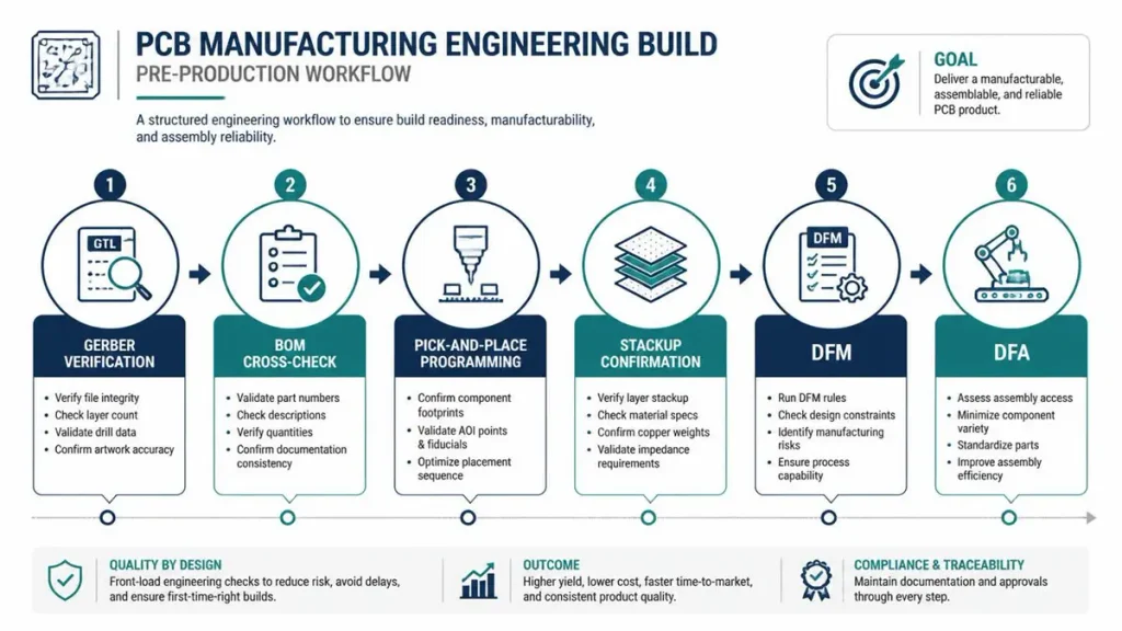
PCB Manufacturing Engineering Build Pre-Production Workflow
Engineering build is a six‑point technical review — Gerber verification, BOM cross‑check, pick‑and‑place programming, stackup confirmation, DFM, and DFA — completed before a single panel is fabricated, and it is where 60–70% of first‑pass yield loss is prevented at the source rather than caught downstream.
This is the stage buyers most often underestimate, because it produces no physical part — only a risk report. But it is where a manufacturing engineer earns their keep.
Gerber and CAM review. Our CAM engineers run incoming Gerber/ODB++ data through DFM software (Valor/Genesis‑class tooling) checking annular ring, minimum trace/space against the fabricator’s process capability (we hold 3/3 mil trace/space in volume, 2/2 mil on select HDI lines), copper balance across the panel, and acid‑trap or slivers in the copper pour. A common pain point here: designs from teams without in‑house fab experience frequently spec 4 mil trace/space on a 12‑layer stackup with 1oz copper — a combination that drops yield sharply once you account for etch‑factor undercut on inner layers. We flag this before tooling, not after 500 panels are scrapped.
BOM verification. Every line item is cross‑checked for AVL (Approved Vendor List) status, lifecycle status (active vs. NRND vs. EOL), and — critically for buyers right now — lead time volatility. In the current passive‑component and MLCC market, a BOM locked six months ago can have three line items that are now 20+ week lead time or obsolete. We run a component risk scan at BOM intake specifically to surface this before it stalls a build.
Pick‑and‑place programming and stackup confirmation. Placement coordinates, rotation offsets, and polarity are programmed and simulated against the actual feeder/nozzle configuration of the target SMT line — not a generic simulation. Stackup is confirmed against the fabricator’s actual laminate library (Isola FR408HR, Panasonic Megtron 6, or standard FR‑4 depending on the impedance and Dk/Df requirement) rather than a “typical” stackup pulled from a template.
DFM (Design for Manufacturability) and DFA (Design for Assembly). DFM review checks fabrication risk: minimum hole size vs. board thickness aspect ratio (we flag anything exceeding 10:1 for standard drilling, since beyond that you’re into controlled‑depth or laser‑drilled microvia territory), soldermask dam width between fine‑pitch pads, and thermal relief on ground planes. DFA checks assembly risk: component‑to‑component spacing for post‑reflow rework access, tombstoning risk on 0201/01005 passives from pad asymmetry, and connector keep‑out zones for fixture clearance.
Exit criteria for this stage: a signed‑off DFM/DFA report with all flagged items dispositioned (accepted‑as‑is, or design change requested), a locked BOM with substitution options pre‑approved for at‑risk parts, and a confirmed stackup with impedance targets calculated — not assumed.
What Happens During Prototype Manufacturing, and What Does It Actually Prove?
Prototype manufacturing produces a small, fully representative batch — typically 5–50 units — through real fabrication and SMT/THT assembly equipment (not a benchtop mockup), specifically to prove that the engineering‑build assumptions hold on physical hardware before committing to tooling and volume purchasing.
This is where paper risk becomes physical evidence. Our prototype builds run on the same equipment class as production — the same LDI (Laser Direct Imaging) exposure system used in production for line‑width control down to ±10% of the target trace width, the same SMT placement lines with ±25 μm placement accuracy on 01005‑class components — because a prototype built on different equipment doesn’t actually validate the production process.
PCB fabrication at prototype scale. Small‑panel fabrication runs through the identical drilling, plating (we hold 20–25 μm minimum copper plating in through‑holes per IPC‑6012 Class 2/3), and etching sequence as volume production. Impedance coupons are cut and TDR‑tested on every prototype lot — we don’t estimate impedance from stackup calculation alone; we measure it, because resin content variance between lamination cycles can shift impedance by several ohms even on an identical stackup design.
SMT assembly and THT. Reflow profiles are developed specifically for the board’s thermal mass — not pulled from a generic profile library. A board mixing a 6‑layer heavy‑copper section with fine‑pitch BGA is a real scenario we see often: the heavy‑copper area acts as a heat sink during reflow, and without a tailored profile (extended soak zone, adjusted ramp rate) you get cold solder joints on the BGA corner balls that don’t show up until thermal cycling. THT components — connectors, electrolytic capacitors — go through wave or selective soldering with a paste‑in‑hole or through‑hole reflow decision made based on component thermal tolerance.
Rework and first‑article inspection. Any deviation caught here — a shifted component, a solder bridge on 0.4mm pitch QFN — is reworked under microscope and logged. This log becomes production‑line training data: if the same defect pattern shows up in prototype, we adjust the stencil aperture or placement program before it ever reaches a production panel.
Exit criteria: electrical continuity/isolation on 100% of prototype units, measured impedance within ±10% of target on coupon testing, and a documented rework log with root cause assigned to every deviation — not just “fixed and shipped.”
How Do You Validate a New Board Design Before It Reaches Volume Production?
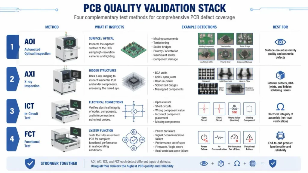
PCB Quality Validation Stack: Four Complementary Test Methods
Validation applies four layered test methods — AOI, X‑ray, ICT, and FCT/electrical testing — because each catches a different failure class that the others miss, and running only one (as many low‑cost suppliers do) leaves entire categories of latent defects undetected until the field.
This stage is where we see the widest quality gap between suppliers, because full four‑method validation costs more in equipment and cycle time than a supplier running AOI alone. Here’s what each method actually catches, and what it misses:
- AOI (Automated Optical Inspection): Catches surface‑visible defects — missing components, wrong polarity, solder bridging, tombstoning, insufficient solder — at typical detection rates above 98% for these defect classes on a well‑programmed system. Misses: anything hidden under a package, meaning it is structurally blind to BGA and QFN solder joint quality.
- X‑ray inspection (AXI): This is the non‑negotiable complement to AOI. 5‑axis X‑ray with oblique‑angle imaging inspects BGA ball voiding (we hold IPC‑A‑610 Class 2 voiding limits under 25% per ball, tighter for Class 3/automotive work), head‑in‑pillow defects, and QFN thermal‑pad solder coverage — all invisible to a camera. Misses: functional/parametric performance.
- ICT (In‑Circuit Test): A bed‑of‑nails or flying‑probe fixture verifies every component’s value, orientation, and solder‑joint electrical connection against the BOM — typically achieving 85–95% test coverage on a well‑designed test‑point layout. Common pain point: boards laid out without test‑point access (a real and frequent issue when the ECAD team designs without DFT input) can drop ICT coverage to below 60%, forcing reliance on functional test alone to close the gap — which is a known risk, not a theoretical one.
- FCT (Functional/Circuit Test) and electrical testing: Powers the board and exercises it against the actual end‑application logic — verifying that a power rail holds regulation under load, that a communication interface achieves target bit‑error‑rate, or that an analog front‑end meets its accuracy spec. This is where a board that “passes ICT” but was designed with a marginal component tolerance stack‑up gets caught.
A scenario worth naming directly: we’ve had incoming boards from other suppliers’ NPI runs that passed AOI and ICT cleanly, but failed FCT intermittently under thermal load — traced to BGA voiding above 30% on a single ground‑return ball, invisible without X‑ray. That defect class is exactly why we run all four methods as standard on NPI validation, not as an optional upsell.
Exit criteria: a validation report cross‑referencing all four test methods against IPC‑A‑610 acceptance criteria for the specified class, with any failure mode root‑caused before pilot production is authorized.
What Is Pilot Production, and How Does It Differ From the Prototype Stage?
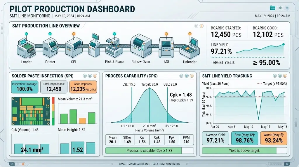
Pilot Production Dashboard: SMT Line Monitoring, SPI, and Cpk Analysis
Pilot production runs a mid‑volume batch — commonly 200–2,000 units, depending on program size — specifically to prove the process is repeatable under real production‑line conditions (shift changes, operator variation, panel‑to‑panel material variance), which a 20‑unit prototype run cannot demonstrate.
This is the stage most often skipped by suppliers under schedule pressure — and it’s the single biggest predictor of a rough production ramp when it’s skipped.
Process validation. We run process capability studies (Cpk) on critical parameters — reflow zone temperatures, solder paste volume via SPI (Solder Paste Inspection, measuring deposit height and area against a target with typical ±15% tolerance windows), and press‑fit or wave‑solder parameters for THT‑heavy assemblies. A Cpk below 1.33 on any critical parameter at this stage is a signal that the process is not ready for full production, not a number we round up and move past.
Yield monitoring. First‑pass yield (FPY) is tracked lot‑by‑lot through the pilot run, not aggregated at the end. A declining FPY trend across pilot lots — say, dropping from 97% to 92% over three consecutive lots — is a leading indicator of a wearing tool, a drifting stencil, or a marginal component lot, and we investigate it during pilot specifically because catching that trend now costs a few hundred units, not tens of thousands.
Assembly optimization. Cycle time per panel, changeover time between product variants (relevant for buyers running mixed‑model lines), and operator ergonomics at manual insertion or inspection stations are measured and tuned. A placement program that runs fine at prototype’s low panel count can reveal feeder‑starvation bottlenecks once you’re running continuous production‑rate panels through the line — pilot is where that gets fixed.
Test validation. ICT and FCT fixtures — often custom‑built for the specific board — are validated for repeatability (gauge R&R) across multiple operators and shifts, confirming the test itself isn’t introducing false failures or false passes.
Exit criteria: demonstrated Cpk ≥1.33 on critical process parameters, stable FPY across at least three consecutive pilot lots, and validated test fixtures with documented gauge R&R results.
What Does “Production Release” Actually Lock Down Before Full‑Scale Manufacturing?
Production release formally freezes five deliverables — manufacturing documentation, an approved BOM, process parameters, quality requirements, and a documented production transfer package — turning everything learned across the previous four stages into a controlled baseline that cannot silently drift once volume orders start.
This is the deliverable buyers should actually ask to see before placing a production PO — not just a sample report.
- Manufacturing documentation: Complete work instructions, reflow/wave profiles, and inspection procedures specific to this part number, version‑controlled.
- Approved BOM: The BOM as validated through pilot, with approved alternates for at‑risk components already qualified — not a promise to “find a substitute if something goes obsolete.”
- Process parameters: The exact, locked settings proven during pilot — squeegee pressure and speed for paste printing, reflow profile by zone, placement force by component package — stored as the production baseline, with any future change requiring a formal ECN (Engineering Change Notice), not a floor‑level adjustment.
- Quality requirements: Acceptance criteria (IPC Class 2 vs. Class 3, specific AQL sampling plans for incoming inspection, in‑process, and outgoing) documented per part number.
- Production transfer: A formal handoff package to the volume production line, including first‑article inspection reports from the pilot run as the accepted baseline sample.
Once release is signed, we treat any change to BOM, process, or supplier of record as a controlled ECN event — not a silent substitution. This is the guardrail that protects a buyer from the most common volume‑production failure mode: a part getting quietly swapped for a “form‑fit‑function equivalent” that behaves differently under a specific load or temperature condition the original part was actually validated against.
Frequently Asked Questions From PCB and PCBA Buyers
What’s the difference between NPI manufacturing and standard PCB prototyping?
Standard prototyping delivers a working board. NPI manufacturing delivers a validated, repeatable process for building that board at volume — including documented DFM/DFA sign‑off, four‑method validation (AOI, X‑ray, ICT, FCT), and a pilot run proving process capability (Cpk ≥1.33) before full production is authorized. Prototyping answers “does it work?”; NPI answers “can we build 50,000 of these with consistent yield?”
How long does a full NPI manufacturing cycle typically take?
For a moderate‑complexity board (8–12 layers, mixed SMT/THT, one or two BGAs), engineering build through production release typically runs 4–8 weeks, depending on component lead times uncovered during BOM risk review and how many DFM issues require design iteration. Simple 2–4 layer boards with a mature BOM can move faster; boards with HDI microvia structures, high pin‑count BGAs, or long‑lead RF components run longer
Why does X‑ray inspection matter if my board already passes AOI and ICT?
Because AOI and ICT are both structurally blind to defects hidden under a package. BGA voiding, head‑in‑pillow joints, and QFN thermal‑pad solder coverage are invisible to a camera (AOI) and often don’t manifest as a hard electrical failure at room temperature (ICT) — they show up as intermittent field failures under thermal cycling or mechanical stress. X‑ray is the only method in the stack that inspects solder joint structure directly.
Can NPI manufacturing help if my component BOM has parts on long lead time or approaching obsolescence?
Yes — this is specifically handled in the engineering‑build stage through BOM risk scanning: every line item is checked against lifecycle status and current lead time, and at‑risk parts get pre‑qualified alternates identified and validated during prototype/pilot, before they become a production‑blocking shortage. Locking a BOM without this check is one of the most common causes of a stalled production ramp.
What should I ask a PCB/PCBA supplier to verify their NPI process is real, not just marketing language?
Ask for: (1) a sample DFM/DFA report showing actual flagged issues from a past program, (2) their standard validation stack — specifically whether X‑ray is standard or an add‑on, (3) Cpk data from a pilot run on a comparable product, and (4) their ECN process for handling a component substitution after production release. A supplier with a mature NPI process will have these on hand without hesitation; one that treats NPI as a sales term usually cannot produce the documentation.
Shenzhen Hongda Circuit Technology Co., Ltd. runs NPI manufacturing for PCB and PCBA programs as a gated, documented process — from engineering build through production release — using in‑house LDI imaging, 5‑axis X‑ray inspection, and SPI‑monitored SMT lines to carry designs from prototype to stable volume production. Email: pcb@pcbkr.com
About Author
David Chen https://www.linkedin.com/in/pcbcoming
David Chen is a Senior RF/PCB Process Engineer at Shenzhen Hongda Circuit Technology Co., Ltd., with over 12 years of experience in high-frequency PCB fabrication, impedance-controlled stack-up design, and Rogers/PTFE laminate processing. He also boasts an extensive professional background in PCBA manufacturing, PCBA testing, and PCBA optimization, with specialized expertise in high-precision PCBA fault analysis and rigorous PCBA reliability testing. The author has worked with high-layer-count server PCB fabrication, ultra-low-loss backplane stackups, and thermo-mechanical reliability optimization for AI infrastructure projects involving 112G and 224G PAM4 architectures. Skilled in complex circuit design and cutting-edge advanced PCB manufacturing processes, he delivers solutions that elevate product durability and performance across industrial applications. His technical articles focusing on PCBA manufacturing workflows and testing methodologies are widely cited by industry peers and technical platforms, and have gained attention and recognition from industry colleagues.