AI Server PCB Supplier in China: How to Evaluate Manufacturing Capabilities, Quality and RFQ Readiness
Where Can You Find a Qualified AI Server PCB Supplier in China?
Choosing an AI Server PCB supplier in China requires more than comparing quotations or checking a factory’s maximum layer count. Buyers need a manufacturer capable of handling advanced multilayer structures, fine-line circuits, HDI microvias, high-speed materials, impedance control and demanding quality requirements. Shenzhen Hongda Circuit Technology Co., Ltd. (PCBKR) supports advanced PCB manufacturing with capabilities including up to 104-layer boards, 10–15 μm line/space, 25–75 μm microvia processing, ppm-level defect control, No MOQ, 24/7 DFM support and fast turnaround time. From prototype development to production orders, PCBKR provides PCB fabrication and PCBA assembly for customer-specific AI server hardware projects. Send your design files to sales@pcbkr.com for engineering review and quotation.
1. What Should Buyers Look for in an AI Server PCB Supplier in China?
An AI server PCB supplier should be evaluated against the actual manufacturing requirements of the board, not just a general claim that it supports high-end electronics.
AI server hardware may contain several different PCB types, including accelerator boards, computing boards, switch boards, backplanes, power boards and high-speed daughter cards. Their manufacturing requirements are not interchangeable. A supplier qualified to manufacture a conventional multilayer power board is not automatically qualified for a high-layer, fine-line, impedance-controlled backplane.
Before shortlisting a supplier, buyers should review six areas:
- Manufacturing scope: Does the factory manufacture bare PCBs, assemble PCBAs, or provide both?
- Layer and interconnection capability: Can it manufacture the proposed layer count, sequential lamination, blind or buried vias, and HDI structures?
- Fine-line capability: Can it meet the required trace width, spacing and registration tolerances?
- Material compatibility: Can it process the specified laminate, copper foil, prepreg and hybrid stackup?
- Electrical and quality controls: Can it manage impedance-related manufacturing variables and provide the agreed inspection evidence?
- Production responsiveness: Can it support urgent engineering reviews, prototypes, small orders and repeat production?
PCBKR provides advanced PCB manufacturing capabilities of up to 104 layers, 10–15 μm line/space and 25–75 μm microvia processing. Its service model also includes No MOQ, 24/7 DFM support and fast turnaround time.
These capabilities are particularly relevant to OEMs and engineering teams developing AI server boards with complex routing, high component density and demanding interconnection requirements.
For buyers who want to understand the specific fabrication and assembly scope, see our AI server PCB manufacturing services.
2. Which AI Server PCB Manufacturing Requirements Should Be Confirmed Before RFQ?
The same product description can represent very different manufacturing workloads. An RFQ that only states “AI server PCB” does not provide enough information for a reliable quotation.
Purchasing and engineering teams should confirm the following specifications before requesting a formal quote:
| Requirement | Information to provide |
|---|---|
| Board type | Accelerator board, backplane, switch board, power board or daughter card |
| Layer count | Total layers and proposed layer arrangement |
| Finished thickness | Nominal thickness and tolerance |
| Board dimensions | Finished size, outline and panelization requirements |
| Base material | Exact laminate and prepreg grades, if specified |
| Copper weight | Starting copper and required finished copper thickness |
| Trace and spacing | Minimum design values and critical routing areas |
| Via structure | Through vias, blind vias, buried vias, microvias or via-in-pad |
| Impedance | Single-ended and differential targets, tolerances and controlled nets |
| Surface finish | ENIG, immersion silver, OSP or another specified finish |
| Back-drilling | Via map, target depth, residual stub requirement and tolerance |
| Quality requirements | IPC class, inspection plan, electrical test and reporting requirements |
| Quantity | Prototype quantity, pilot volume and forecast production volume |
PCBKR’s advanced manufacturing capabilities include up to 104-layer PCB structures, 10–15 μm line/space and 25–75 μm microvia processing. These capabilities allow the factory to evaluate demanding multilayer and HDI constructions for AI server applications.
Buyers should still provide their actual stackup, material and electrical specifications. This enables engineering to confirm the applicable process route and identify any design details that need attention before production.
A useful RFQ should distinguish between mandatory specifications and preferred design targets. If the manufacturer proposes a change to line width, spacing, dielectric thickness, material grade or via structure, the change should be documented and approved before production data is released.
3. Can the Supplier Manufacture High-Layer AI Server PCBs?
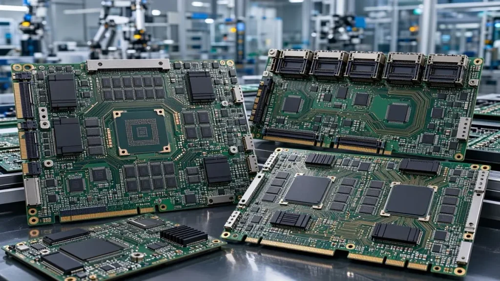
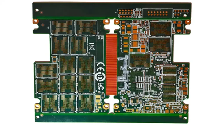
High-layer AI server PCBs featuring complex multilayer structures, high-density interconnections, and advanced backplane designs for AI computing infrastructure.
High-layer PCB manufacturing involves more than adding additional copper layers. As layer count and board thickness increase, the manufacturing process must manage inner-layer registration, lamination consistency, drilling accuracy, plating, etching and finished-board dimensional stability.
For an AI server PCB project, buyers should ask the supplier to review:
- Total layer count and individual layer construction.
- Core and prepreg thickness distribution.
- Copper distribution and layer-to-layer registration requirements.
- Board thickness and aspect ratio.
- Mechanical drilling and plating requirements.
- Lamination sequence and any sequential lamination steps.
- Finished-board flatness and dimensional tolerances.
- Electrical test and inspection requirements.
PCBKR supports high-layer PCB manufacturing up to 104 layers. This capability is relevant to complex server boards and high-density multilayer constructions where layer arrangement, registration, lamination and drilling accuracy are critical.
For high-layer designs, the manufacturing review should consider more than the total layer count. Board dimensions, thickness, copper distribution, via structure, material system and electrical requirements all influence the production process.
Buyers should provide the proposed construction and request confirmation of the applicable process route, including the material combination, finished thickness, via structure and inspection requirements.
4. How Does HDI and Microvia Capability Affect AI Server PCB Manufacturing?
HDI technology is used when component density, package escape routing or interconnection requirements cannot be addressed efficiently with conventional through-hole structures.
Depending on the design, an AI server board may use blind vias, buried vias, laser-drilled microvias, stacked or staggered via structures, and via-in-pad constructions. These features can increase routing density, but they also introduce additional process controls.
Buyers should verify:
- Whether the required microvia diameter is compatible with the proposed dielectric thickness.
- Whether the design requires stacked or staggered microvias.
- Whether sequential lamination is needed.
- Whether via filling and capping are specified.
- Whether via-in-pad structures require additional planarization or inspection.
- Whether the proposed structure has a suitable reliability qualification plan.
PCBKR supports advanced microvia processing in the 25–75 μm range, with laser processing capabilities that include Mitsubishi UV/CO₂ laser drilling at a 75 μm target with ±5 μm tolerance and picosecond laser processing down to 50 μm.
These capabilities support demanding HDI manufacturing requirements. The appropriate process depends on dielectric thickness, via geometry, aspect ratio, copper plating and reliability requirements.
For a more detailed discussion of HDI structures and manufacturing considerations, see our HDI PCB manufacturing guide for AI servers.
5. How Are High-Speed Materials and Stackups Evaluated?
Material selection affects dielectric loss, impedance, insertion loss, thermal behavior, dimensional stability and manufacturing cost. A supplier should not recommend a laminate based only on its brand name.
For high-speed AI server boards, the engineering review may need to consider:
- Dielectric constant (Dk) and dissipation factor (Df).
- Copper foil profile and surface roughness.
- Glass-weave construction and potential skew effects.
- Core and prepreg thickness.
- Resin content and lamination compatibility.
- Copper weight and finished dielectric spacing.
- Hybrid stackup compatibility.
- Material availability and approved alternatives.
Materials such as Megtron-series laminates, I-Tera MT40 and other low-loss materials may be specified for particular high-speed designs. The actual grade must be confirmed against the customer’s drawings, stackup and electrical requirements.
If a specified laminate is unavailable, a substitute should not be introduced simply because its published Dk or Df appears similar. The proposed alternative may change impedance, insertion loss, thermal behavior and the lamination process.
A controlled material substitution process should include:
- Identification of the original material and the proposed alternative.
- Comparison of relevant electrical and mechanical properties.
- Review of the revised stackup and impedance calculations.
- Customer approval before material substitution.
- Additional validation if required by the project specification.
For procurement, material availability should be confirmed before the production schedule is committed. A quotation should state whether the price and lead time assume a specific laminate grade, an available inventory lot or a future material purchase.
6. How Does the Factory Control Impedance and Signal-Related Manufacturing Risks?
Controlled impedance is a manufacturing requirement, but it is not the same as guaranteeing the signal integrity of a complete server system.
The manufacturer controls physical parameters that influence impedance, including dielectric thickness, trace width, copper thickness, etching compensation, material properties and stackup construction. The design team remains responsible for defining the electrical requirements and system-level channel performance targets unless additional engineering services are explicitly included in the project scope.
Before production, buyers should confirm:
- Which nets require controlled impedance.
- The single-ended or differential impedance targets.
- The specified tolerance.
- The reference plane and routing layer for each controlled net.
- The material and dielectric assumptions.
- Whether impedance coupons are required.
- The test method and reporting format.
- Whether any proposed geometry or stackup changes require written approval.
PCBKR has VNA testing capability up to 70 GHz. This equipment capability can support agreed high-frequency measurement tasks, subject to the test fixture, calibration, coupon design, method and project requirements.
A VNA measurement does not by itself certify a complete 112G or 224G PAM4 channel, validate the full server interconnect, or guarantee system-level signal integrity. Those conclusions require the appropriate design data, test configuration and system-level validation.
For buyers evaluating high-speed backplane projects, our 224G AI server backplane PCB design guide discusses the related design and manufacturing considerations.
7. Which Manufacturing Processes Should an AI Server PCB Supplier Demonstrate?
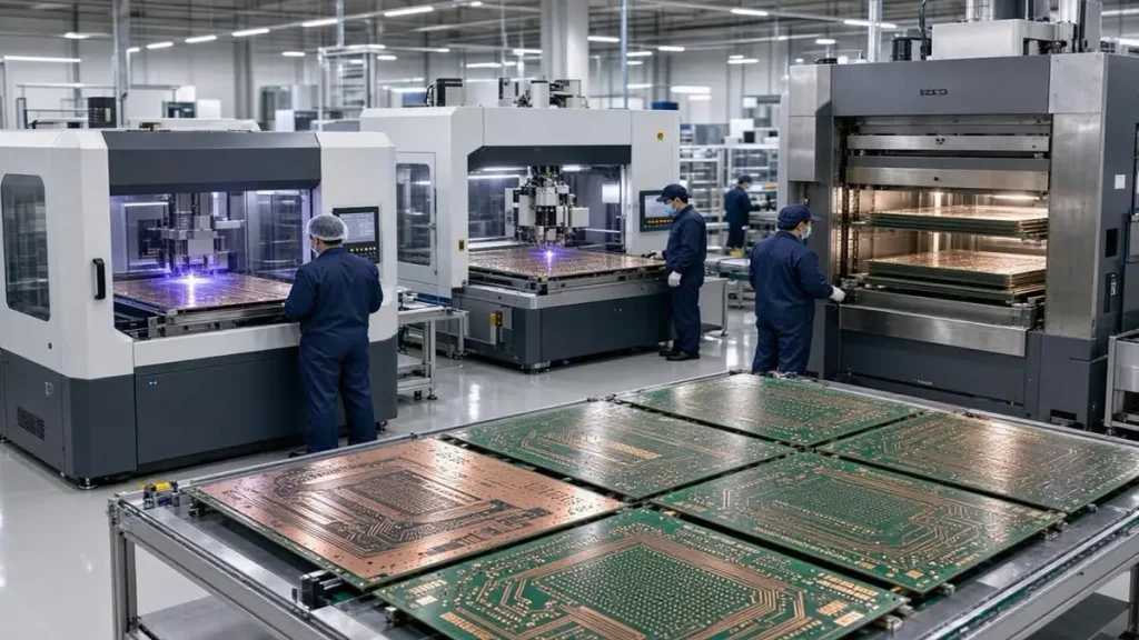
Advanced AI server PCB manufacturing processes, including precision laser direct imaging, microvia drilling, multilayer vacuum lamination, and fine-line circuit formation.
A supplier should explain how its equipment and process controls relate to the actual board construction. A list of machine names without process context is not sufficient.
Relevant process areas include:
Pattern imaging and fine-line processing
PCBKR uses SCREEN Ledia LDI equipment, with a confirmed 8 μm target and ±10 μm process parameter. Its advanced fine-line manufacturing capability supports 10–15 μm line/space requirements, subject to the applicable copper construction, layer, design density and process conditions.
PCBKR also has mSAP capability at 8/8 μm, established since Q3 2024. This provides an additional process route for fine-line circuit manufacturing.
Laser drilling
Mitsubishi UV/CO₂ laser drilling is used for microvia processing, with a confirmed 75 μm target and ±5 μm tolerance. Picosecond laser processing is available down to 50 μm. PCBKR’s microvia capability supports 25–75 μm design requirements, with the applicable process selected according to the via structure and dielectric construction.
Lamination
PCBKR’s LAUFFER lamination system supports pressure settings of 80, 150 and 200 psi, with vacuum below 50 mbar. The actual lamination recipe depends on the material system, stackup and process qualification.
Copper plating and circuit formation
The plating and circuit formation process must be evaluated against the required copper thickness, via structure, aspect ratio and finished-board specifications. Buyers should request confirmation of the specific construction rather than assume that one equipment specification covers every board design.
For more information about the equipment and process areas used in PCB production, see PCB manufacturing equipment and process capabilities.
8. How Should Buyers Verify PCB Inspection and Quality Control?
Quality claims should be supported by inspection methods, acceptance criteria and records. A statement such as “strict quality control” does not tell a buyer what will actually be inspected.
For AI server PCB projects, the inspection plan may include:
| Inspection or test | What it helps verify |
|---|---|
| AOI | Circuit pattern defects and visible process issues |
| 3D AOI | Three-dimensional inspection of applicable features |
| X-ray inspection | Internal structures and hidden features, depending on the application |
| Flying probe electrical test | Electrical continuity and isolation |
| Four-wire Kelvin measurement | Low-resistance measurement where specified |
| Impedance testing | Compliance with the agreed impedance test plan |
| VNA measurement | Frequency-dependent electrical measurement under an agreed setup |
| Cross-section analysis | Internal copper, dielectric and via structure when required |
PCBKR has 3D AOI, X-ray, four-wire Kelvin flying probe and VNA testing capabilities. Its quality-control approach supports demanding PCB manufacturing requirements, including ppm-level defect control for applicable production programs.
Buyers should confirm the applicable quality target, measurement method, sampling plan and reporting format for their specific project. PPM performance should be evaluated using an agreed defect definition, inspection scope and production data rather than an undefined headline number.
Buyers should also agree on the required deliverables, such as:
- Electrical test report.
- Impedance test report and coupon details.
- Material certificates or material identification records, where required.
- Dimensional inspection report.
- Cross-section report, if specified.
- Nonconformance and corrective-action records.
- Final inspection and shipment documentation.
The supplier should clarify the acceptance criteria, sampling frequency and responsibility for any tests that must be completed by the customer or an independent laboratory.
9. What Manufacturing Evidence Should Buyers Request From a China PCB Supplier?
A qualified supplier should be able to provide evidence relevant to the actual project. Buyers do not need an impressive equipment catalogue; they need records that demonstrate control of the required construction.
A practical supplier qualification review can request:
1. Process capability evidence
Ask for the applicable process limits for layer count, board thickness, copper weight, trace and spacing, via structure, drilling and registration. PCBKR’s advanced capability scope includes up to 104 layers, 10–15 μm line/space and 25–75 μm microvia processing.
2. Equipment and process information
Request a description of the equipment used for imaging, lamination, drilling, plating, inspection and electrical testing. Confirm that the equipment is located at the manufacturing facility responsible for the order.
3. Quality system documentation
Request relevant certificates and confirm their issuing organization, validity, site coverage and scope. A certificate should not be assumed to cover every product or every customer requirement.
4. Inspection records
Ask for representative AOI, X-ray, electrical test, impedance or cross-section reports when relevant. Sensitive customer information can be redacted, but the report should still demonstrate the inspection method and result format.
5. Production traceability
Confirm how the factory identifies material batches, production lots, engineering revisions, inspection records and nonconforming products.
6. Engineering change control
Ask how proposed changes to material, stackup, artwork, drilling, surface finish or process parameters are submitted and approved.
A supplier should not use a general capability statement as a substitute for project-specific evidence. The most useful qualification records are those that match the board’s actual construction and acceptance requirements.
10. Can the Supplier Support Prototype, Small-Batch and Mass Production?
Prototype capability and repeat-production capability are related, but they are not identical.
A prototype order is often used to confirm manufacturability, dimensional accuracy, electrical performance and assembly compatibility. A production release introduces additional requirements, including process repeatability, material planning, revision control and inspection consistency.
PCBKR supports projects from prototype development to small-batch and production orders. Its No MOQ service model allows customers to discuss low-quantity requirements without being restricted by a standard minimum order quantity.
The factory also provides 24/7 DFM support to help engineering and purchasing teams address manufacturing questions, identify potential design risks and accelerate project communication.
For urgent development schedules, PCBKR’s fast turnaround approach helps customers move through engineering review and prototype manufacturing efficiently. Actual delivery timing depends on board complexity, material availability, process requirements, quantity and inspection scope.
A practical project workflow includes:
Engineering review
The supplier reviews the Gerber data, stackup, drilling information, impedance requirements and manufacturing notes. Open issues should be listed and resolved before production release.
Prototype fabrication
The first build verifies the proposed construction and identifies issues that may not be visible during the initial data review.
First-article review
The customer and supplier review the agreed inspection records, electrical results and any required validation data.
Pilot or small-batch production
The process is checked for repeatability, material consistency, yield-related issues and production documentation.
Repeat production
The approved revision, material requirements, inspection plan and change-control process are maintained for subsequent orders.
Buyers should ask the factory to confirm the production schedule for the specific board, rather than rely on a general statement that it supports mass production.
11. What Determines AI Server PCB Cost and Manufacturing Lead Time?
AI server PCB pricing depends on the construction and process route, not just the finished board size or quantity.
Important cost drivers include:
- Number of layers and board dimensions.
- Laminate grade and copper foil selection.
- Finished copper thickness.
- Fine-line requirements.
- Blind, buried and microvia structures.
- Sequential lamination requirements.
- Back-drilling and via filling.
- Surface finish.
- Impedance testing and additional inspection.
- Prototype quantity, panel utilization and production volume.
- Material availability and procurement conditions.
PCBKR’s No MOQ policy provides flexibility for prototype and low-volume purchasing. However, the unit price of a small order may differ from that of a larger production quantity because of setup, engineering and material utilization costs.
Fast TTM is important for AI server development, but lead time should be divided into separate stages:
- Engineering and CAM review.
- Material confirmation and procurement.
- PCB fabrication.
- Electrical testing and final inspection.
- PCBA assembly, if included.
- Packaging and shipment.
A short fabrication estimate is not necessarily the same as the total order-to-delivery lead time. Special materials, complex stackups, engineering changes, additional testing and customer approval can all affect the schedule.
For a useful quotation, ask the supplier to state the assumptions behind its price and lead time. These should include the material grade, quantity, approved revision, inspection scope, shipping method and quotation validity period.
12. What Information Should Be Included in an AI Server PCB RFQ?
A complete RFQ reduces repeated clarification and helps the supplier identify manufacturing risks before issuing a quotation.
The following information is recommended:
Design files
- Gerber or ODB++ files.
- NC drill files.
- Fabrication drawing.
- Stackup drawing.
- Impedance table and controlled-net information.
- Back-drill map, if applicable.
Technical specifications
- Layer count and finished board thickness.
- Board dimensions and tolerances.
- Base material and copper weight.
- Minimum trace and spacing.
- Hole and microvia specifications.
- Surface finish.
- Impedance targets and tolerance.
- Electrical test requirements.
- IPC class or customer-specific acceptance criteria.
Commercial information
- Prototype quantity.
- Pilot quantity and forecast annual volume.
- Required delivery date.
- Shipping destination.
- Whether PCB fabrication only or PCBA assembly is required.
- Whether material sourcing is supplier-managed or customer-supplied.
Quality and documentation
- Required inspection methods.
- Test report format.
- Material certification requirements.
- Traceability requirements.
- First-article approval process.
- Change-control and nonconformance requirements.
PCBKR offers No MOQ, 24/7 DFM support and fast turnaround for customer-specific PCB projects. Buyers can submit preliminary design data for an initial engineering review even if the design is not yet finalized.
To discuss an AI server PCB project with Shenzhen Hongda Circuit Technology Co., Ltd., send the available design files and requirements to sales@pcbkr.com. Please include the target quantity, material specification and required delivery schedule where available.
Frequently Asked Questions About AI Server PCB Suppliers in China
How do I choose an AI server PCB supplier in China?
Compare suppliers against the actual board construction, including layer count, HDI structure, material, impedance requirements, inspection plan and production volume. Ask for project-relevant process evidence and confirm how engineering changes, material substitutions and quality issues are controlled. Also compare engineering response time, minimum order quantity and prototype turnaround support.
What is the maximum layer count for AI server PCBs manufactured by PCBKR?
PCBKR supports high-layer PCB manufacturing up to 104 layers. Actual feasibility depends on board dimensions, finished thickness, material system, copper distribution, via structure, registration requirements and lamination process. Buyers should provide the proposed construction for a project-specific manufacturing review.
Can PCBKR manufacture 10–15 μm line/space PCBs?
Yes. PCBKR supports advanced fine-line PCB manufacturing with 10–15 μm line/space capability. Its process portfolio includes SCREEN Ledia LDI and mSAP capability at 8/8 μm. The applicable process route depends on copper construction, layer, design density and project requirements.
Can PCBKR manufacture 25–75 μm microvias for HDI boards?
PCBKR supports microvia processing in the 25–75 μm range. Its laser processing capabilities include Mitsubishi UV/CO₂ laser drilling and picosecond laser processing. Final feasibility depends on dielectric thickness, via geometry, aspect ratio, plating requirements and the proposed HDI construction.
Does PCBKR accept small prototype orders and provide urgent DFM support?
Yes. PCBKR offers No MOQ, 24/7 DFM support and fast turnaround services. These options help OEMs and engineering teams discuss prototype and low-volume requirements without a standard minimum order restriction. Actual delivery time depends on design complexity, material availability, manufacturing route and inspection requirements.
About the Manufacturer
Shenzhen Hongda Circuit Technology Co., Ltd. (PCBKR) provides advanced PCB fabrication and PCBA assembly for customer-specific electronics projects.
Its manufacturing capabilities include up to 104-layer PCBs, 10–15 μm line/space, 25–75 μm microvia processing and high-speed PCB manufacturing support. The company also provides No MOQ, 24/7 DFM support and fast turnaround services for prototype and production projects.
For AI server PCB projects involving multilayer construction, HDI features or high-speed electrical requirements, buyers are encouraged to provide the relevant technical files for engineering review.
RFQ Contact: sales@pcbkr.com
Website: https://www.pcbkr.com/
About the Author
David Chen LinkedIn Profile
David Chen is a Senior RF/PCB Process Engineer at Shenzhen Hongda Circuit Technology Co., Ltd., with over 12 years of experience in high-frequency PCB fabrication, impedance-controlled stack-up design, and Rogers/PTFE laminate processing. He also boasts an extensive professional background in PCBA manufacturing, PCBA testing, and PCBA optimization, with specialized expertise in high-precision PCBA fault analysis and rigorous PCBA reliability testing. The author has worked with high-layer-count server PCB fabrication, ultra-low-loss backplane stackups, and thermo-mechanical reliability optimization for AI infrastructure projects involving 112G and 224G PAM4 architectures. Skilled in complex circuit design and cutting-edge advanced PCB manufacturing processes, he delivers solutions that elevate product durability and performance across industrial applications. His technical articles focusing on PCBA manufacturing workflows and testing methodologies are widely cited by industry peers and technical platforms, and have gained attention and recognition from industry colleagues.