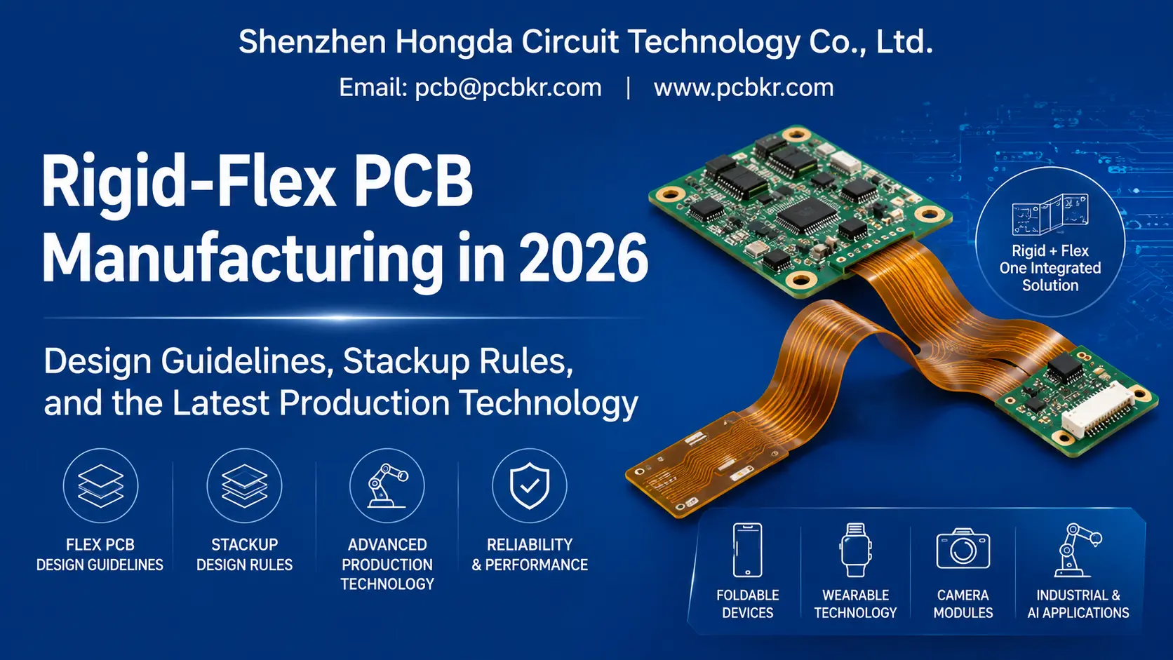
Rigid-Flex PCB Manufacturing in 2026: Flex PCB Design Guidelines, Stackup Rules, and the Latest Production Technology
Choosing between a flex PCB and a rigid-flex PCB is rarely a cosmetic decision — it
determines whether a folding camera module survives 200,000 bend cycles or fails at
20,000. At Shenzhen Hongda Circuit Technology Co., Ltd., our engineering team works
with product designers who need a flexible circuit that holds up in the field, not just on a
datasheet. This guide walks through the design rules, stackup choices, and manufacturing
technology shaping rigid-flex PCB production in 2026, and closes with the questions
procurement teams most often ask before selecting a supplier.
What Is a Rigid-Flex PCB and How Does It Differ From a Flex PCB?
A rigid-flex PCB combines one or more flexible polyimide layers with rigid FR4 sections
laminated into a single, continuous board. The flexible sections act as built-in cabling
between rigid zones, replacing connectors and ribbon cables that would otherwise add
weight, failure points, and assembly time.
A standalone flex PCB, sometimes called a flexible PCB or flexible printed circuit, has no
rigid sections at all — the entire board bends. Rigid-flex is the right call when a product
needs mechanical stability for mounting components (connectors, ICs, shielding cans) at
one or more locations while still folding or flexing between them. Devices like foldable
phones, wearables, and AI-enabled camera modules increasingly specify rigid-flex for
exactly this reason: fewer solder joints, lower z-height, and better vibration resistance than
a rigid board plus a separate flex cable.
The distinction matters at the quoting stage too — a board described loosely as “pcb flex
rigid” in an RFQ can mean either construction, so it’s worth confirming stack composition
before comparing prices across suppliers.
Flex PCB Design Guidelines for 2026: Core Rules Every Engineer Should Follow
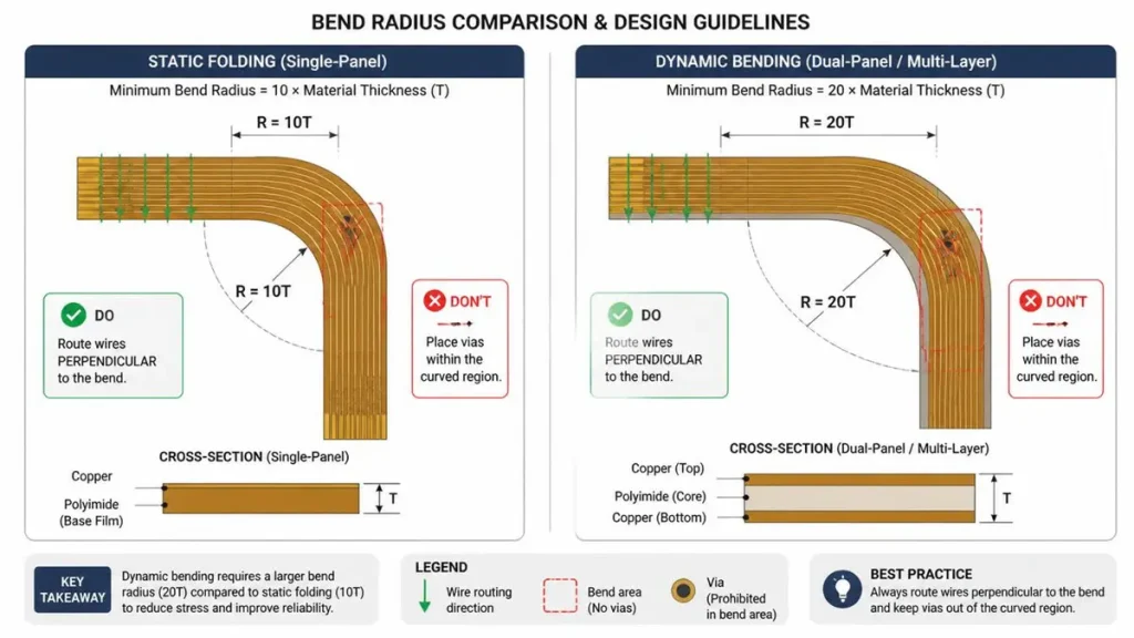
Flex PCB Bend Radius Comparison and Layout Design Guidelines
Flex PCB design guidelines haven’t changed in principle since the technology matured, but
the tolerances have tightened as devices get thinner and bend counts climb into the
hundreds of thousands.
Minimum Bend Radius and Copper Thickness Requirements
The starting rule of thumb is that minimum bend radius should be at least 10 times the total
flex circuit thickness for a single-sided design, and closer to 20 times for double-sided or
multilayer flex. A circuit built for one-time installation bending (static) can tolerate a
tighter radius than one designed for continuous dynamic flexing — a hinge that opens and
closes thousands of times a day needs a radius closer to 40–100 times the material
thickness to avoid fatigue cracking.
Copper thickness is the second lever. Standard options run from 12µm (1/3 oz) up to 35µm(1 oz); thinner foil bends more easily and resists fatigue cracking longer, but it also raisesresistance and limits current-carrying capacity. For dynamic-flex applications we generallyrecommend rolled annealed copper at 12–18µm rather than defaulting to 1 oz foil out of habit.
Trace Routing and Coverlay Design in Flex PCB Layouts
Traces should run perpendicular to the bend line, never parallel to it — a trace that crosses
the fold at an angle distributes stress far more evenly than one that runs straight along the
bend axis. Staggering trace widths and adding teardrop pads at via transitions further
reduces stress concentration at the exact points where cracking tends to start.
Coverlay — the polyimide film that replaces solder mask on flexible sections — typically
runs 25–50µm thick with an adhesive layer bonded under heat and pressure. Coverlay
openings for pads should be sized with enough annular ring to prevent adhesive squeeze
out from encroaching on the exposed copper, a detail that shows up repeatedly in first
article rejections when it’s overlooked.
RA Copper vs ED Copper: Choosing the Right Foil for Flexible Circuits
Rolled annealed (RA) copper has an elongated, fibrous grain structure that flexes without
cracking, making it the standard choice for any circuit that bends repeatedly in service.
Electrodeposited (ED) copper has a more brittle, columnar grain structure — it’s cheaper
and perfectly adequate for static, install-once-and-forget flex applications, but it’s the
wrong choice for a hinge or a moving robotic arm. Specifying RA vs ED copper explicitly on
the fab drawing, rather than leaving it to the manufacturer’s default, avoids a common
source of early-life field failures.
Flex PCB Stackup Design: Adhesive, Adhesiveless, and Shielding Options
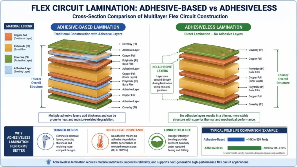
Multilayer Flex PCB Design – Adhesive-Based vs. Adhesiveless Lamination Cross-Section
Flex PCB stackup construction generally falls into three categories: single-layer, double
layer, and multilayer, with the layer choice driven by circuit density and impedance
requirements rather than cost alone.
Within any of these, the base laminate can be adhesive-based (copper bonded to polyimide
with an acrylic or epoxy adhesive) or adhesiveless (copper deposited or cast directly onto
the polyimide). Adhesiveless construction is thinner, handles higher temperatures, and
flexes more consistently over the long term — it costs more up front but is now the default
recommendation for any board rated for more than 50,000 bend cycles.
Where EMI is a concern, shielding is added either as a sputtered or laminated shield film
over the flex layer, or through selective ground-plane stitching. Sputtered shielding keeps
the flex section thinner and more bendable than a laminated foil shield, which matters on
tightly folded camera and antenna modules.
DFM for Rigid-Flex PCB Manufacturing: Panel Utilization and Stiffener Design
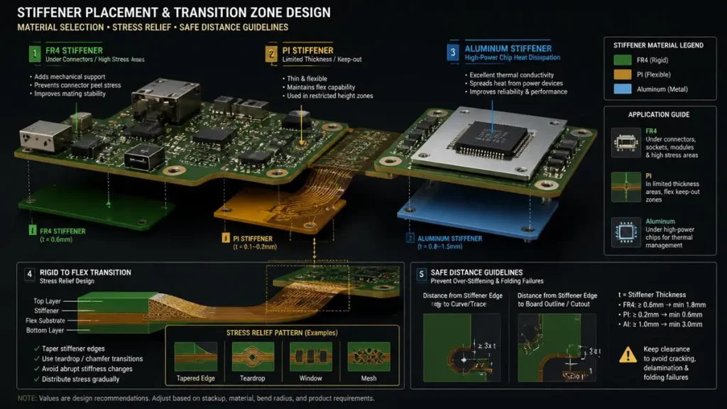
Flex PCB Design – 3D Deconstructed View of Stiffener Placement and Transition Zone Stress Relief
Design for manufacturability on rigid-flex boards comes down mostly to panel efficiency
and reinforcement at the rigid-to-flex transition.
Stiffener Design With FR4, Polyimide, and Aluminum Reinforcement
A stiffener is a non-conductive backing layer bonded under connectors, ICs, or mounting points on the flex section to keep them from flexing during assembly and use. FR4 stiffeners are the low-cost default for connector backing; polyimide stiffeners are thinner and used where board thickness is tightly constrained; aluminum stiffeners add heat sinking alongside mechanical support, useful under high-power components. Stiffener thickness and adhesive selection should be specified per zone, not applied uniformly across the board, since over-stiffening a bend area defeats the purpose of using flex in the first place.
Via and Coverlay Opening Restrictions in Multilayer Flex Boards
Vias placed inside a bend zone are one of the most reliable ways to guarantee a field failure
— plated through-holes concentrate mechanical stress and crack under repeated flexing.
Vias, and ideally components, should stay confined to rigid or static-flex zones, with only
continuous copper traces crossing the dynamic bend. Coverlay openings near a bend also
need extra clearance from the fold line to avoid delamination at the adhesive edge.
Dynamic vs Static Flex Applications: How to Design Flex PCB for the Right Use Case
Whether a board is dynamic or static changes almost every design decision above, so it’s
worth settling this early rather than defaulting to “flex-capable” specs across the board.
Static applications — a flex circuit folded once during assembly and never moved again —
can use ED copper, tighter bend radii, and standard adhesive laminates without much risk.
Dynamic applications — foldable hinges, robotic arm cabling, camera gimbals — need RA
copper, generous bend radii, adhesiveless laminate, and trace geometry validated against
the actual expected cycle count, not just a generic flex PCB template. Knowing how to
design flex PCB for the correct duty cycle up front is far cheaper than redesigning after a
reliability failure in the field.
How Flex PCB Manufacturing Works: From Laser Imaging to Lamination
Understanding how flex PCB manufacturing actually happens on the shop floor makes it
easier to write a spec the fab can actually hold to.
Modern flex and rigid-flex production starts with laser direct imaging (LDI) rather than
photo-tooling, giving tighter line-width control on the fine traces flex layouts demand.
Layers are laminated in sequence — flex cores first, then rigid FR4 sections bonded around
them under controlled heat and pressure — followed by drilling, plating, and coverlay
application specific to the flexible zones. Automated optical inspection with machine
learning-assisted defect classification has become standard on multilayer rigid-flex lines in
2026, catching micro-cracks and copper voids that manual inspection routinely missed a
few years ago.
Newer capabilities gaining traction this year include embedded passive components within
rigid sections to shrink board footprint, halogen-free polyimide and coverlay materials for
compliance-driven customers, and high-density interconnect (HDI) techniques adapted for
flex layers to support the trace densities that camera modules and compact wearables now
require.
Impedance Control for High-Speed Flex PCB in AI and 5G Hardware
High-speed signal integrity on flex layers used to be an afterthought; it no longer can be. AI
accelerator boards, 5G RF modules, and high-resolution camera interconnects all push
differential pairs through flex sections at speeds where trace geometry, dielectric
consistency, and copper roughness directly affect signal loss. Impedance control on flex
PCB requires tighter control over dielectric thickness tolerance and copper foil profile than
a comparable rigid board, since the flexible dielectric is inherently less dimensionally stable
during lamination. Specifying impedance targets with a tolerance band (typically ±10%)
and requesting controlled-impedance test coupons on the production panel is now
standard practice for any flex design carrying high-speed data.
Common Flex PCB Design Failures and Manufacturing Fixes
The failures that show up most often in the field trace back to a small set of root causes:
copper cracking from vias or components placed inside bend zones, delamination at
coverlay edges from insufficient clearance to the fold line, and impedance drift from
dielectric thickness variation during lamination. Each of these is preventable at the design
stage — moving vias out of bend areas, adding proper clearance around coverlay openings,
and validating stackup tolerances before tooling — rather than something to catch during
first-article inspection.
Choosing a Reliable Flex PCB Manufacturer for Rigid-Flex PCB Production
A flex PCB manufacturer’s process controls matter more on rigid-flex boards than on
standard rigid PCBs, because the failure modes above are largely invisible until a board is
flexed hundreds or thousands of times after assembly. Shenzhen Hongda Circuit
Technology Co., Ltd. applies IPC-6013 class construction standards, RA/ED copper
selection by application, and impedance-controlled lamination across its flex and rigid-flex
lines, with DFM review offered before tooling on every new project. For procurement teams
comparing suppliers, the process controls behind the quote matter as much as the unit
price.
Frequently Asked Questions
What should I check before requesting a quote from a flex PCB manufacturer?
Confirm the layer count and construction (flex-only vs rigid-flex), whether the application is dynamic or static, and whether RA or ED copper is required. Suppliers that ask these questions back before quoting are usually the ones with real flex process experience rather than a rigid-PCB line adapted for flex work,
What is a rigid-flex PCB, and does my product actually need one instead of a standard
flex or rigid board?
A rigid-flex PCB combines rigid and flexible sections in one laminated board, replacing separate connectors and cables between rigid zones. It’s worth the added cost when a product needs both structural mounting points and continuous flexing between them — foldable devices, wearables, and compact camera modules are typical candidates. A simpler product that only needs occasional cable flexing may do fine with a standalone flex PCB.
How do I verify a rigid-flex PCB supplier’s quality certifications and process controls?
Ask for IPC class certification (IPC-6013 for flex/rigid-flex, IPC-A-600 for acceptability),request sample test coupons showing impedance and via reliability data, and ask whether AOI and cross-section analysis are performed on production lots, not only on first-article samples.
What is the typical lead time for rigid-flex PCB prototyping versus mass production?
Prototype rigid-flex boards typically run 7–15 working days depending on layer count and stiffener complexity, while mass production lead times extend to 3–5 weeks once tooling and impedance validation are locked in. Suppliers offering firm quotes without asking about layer count or bend cycle requirements are worth double-checking before committing.
How do I request a DFM (Design for Manufacturability) review before committing to a
rigid-flex PCB order?
Send the fab drawing, stackup, and Gerber files along with a note on
dynamic vs static use and expected bend cycle count — a supplier with genuine flex manufacturing experience should flag via placement inside bend zones, coverlay clearance issues, and copper type mismatches during DFM review rather than after tooling is cut.
About Author
David Chen https://www.linkedin.com/in/pcbcoming
David Chen boasts an extensive professional background in PCBA manufacturing, PCBA testing, and PCBA optimization, with specialized expertise in high-precision PCBA fault analysis and rigorous PCBA reliability testing. The author has worked with high-layer-count server PCB fabrication, ultra-low-loss backplane stackups, and thermo-mechanical reliability optimization for AI infrastructure projects involving 112G and 224G PAM4 architectures. Skilled in complex circuit design and cutting-edge advanced PCB manufacturing processes, he delivers solutions that elevate product durability and performance across industrial applications. His technical articles focusing on PCBA manufacturing workflows and testing methodologies are widely cited by industry peers, research institutions, and technical platforms, solidifying his reputation as a recognized technical authority in the global circuit board manufacturing sector.