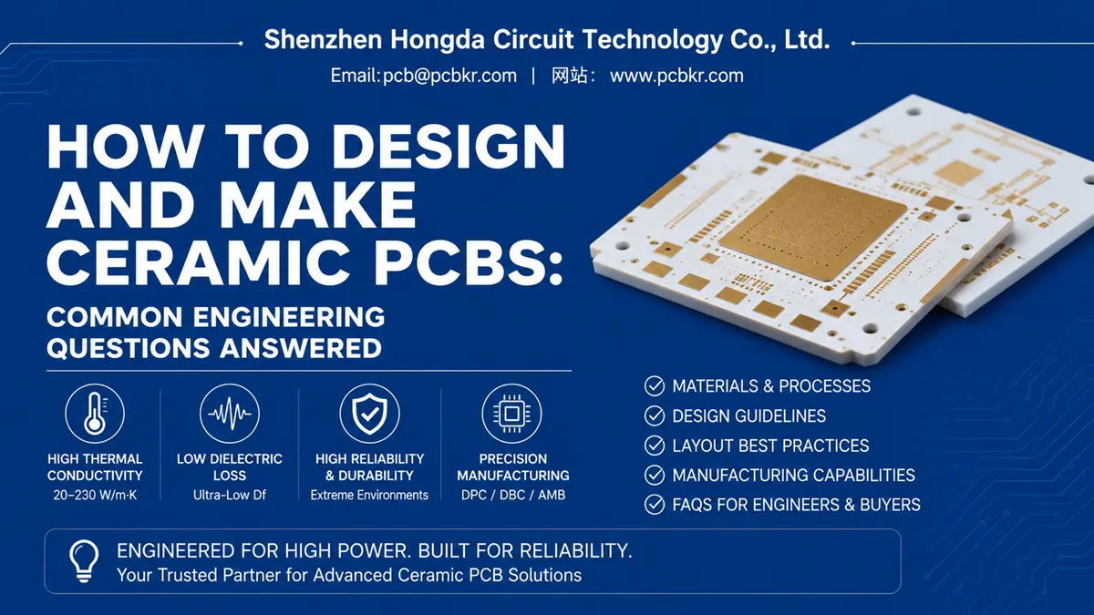
How to Design and Make Ceramic PCBs: Common Engineering Questions Answered
Custom ceramic circuit board solutions deliver exceptional thermal conductivity (20-230 W/m-K) and ultra-low dielectric loss compared to FR4. Successful deployment of these advanced substrates requires matching specific application profiles to processing technologies—Direct Plated Copper (DPC) for sub-micron fine-line precision, or Direct Bonded Copper (DBC) and Active Metal Brazing (AMB) for high-current power routing. Top-tier yield architectures depend heavily on rigorous DFM optimization, laser direct imaging, and precision lamination.
Introduction
Modern power electronics demand rapid miniaturization alongside extreme power densities. Traditional fiberglass-epoxy substrates fail completely when local thermal dissipation levels exceed the performance limits of standard dielectric systems. This technical limitation is addressed by advanced ceramic circuit board solutions. By replacing high-impedance woven matrix materials with solid ceramic substrates, electronic assemblies achieve thermal dissipation rates tens to hundreds of times faster than standard materials, maintaining structural integrity across extreme operational profiles.
This technical guide provides a clear roadmap tailored for hardware engineers and industrial procurement professionals. We analyze critical design rules, complex fabrication workflows, and material boundaries to help you transition seamlessly from prototyping to volume production. Through close analysis of layout geometries, conductor profiling, and structural data optimization, this article delivers the actionable engineering insights required to optimize modern B2B hardware architectures.
How to Make a Ceramic PCB
What Is the Typical Ceramic PCB Manufacturing Process?
Manufacturing high-reliability ceramic boards requires strict process control, combining metallurgical deposition with specialized post-treatments. The comprehensive industrial fabrication sequence operates through six critical steps:
- Substrate Preparation and Selection: Raw base sheets are chosen based on thermal performance, mechanical load, and target application. Materials include Alumina (Al2O3), Aluminum Nitride (AlN), and Silicon Nitride (Si3N4). Substrates undergo precision laser cutting, scribing, via drilling, and intense chemical cleaning to eliminate micro-particles and surface irregularities.
- Surface Conditioning: Ceramic surfaces undergo micro-etching, polishing, or plasma treatments to optimize surface roughness, creating ideal topography for high-adhesion metallurgical bonds.
- Metallization Deposition: Conductive layers are built using specialized manufacturing techniques depending on design requirements: Direct Bonded Copper (DBC) or Active Metal Brazing (AMB) for heavy current loads; Direct Plated Copper (DPC) for high-density, fine-pitch interconnects; or thick-film screen printing for cost-sensitive standard circuits.
- Photo-Patterning and Chemical Etching: Circuit graphics are transferred via high-precision Laser Direct Imaging (LDI) onto photoresist layers, followed by targeted chemical etching to form clean conductor paths (applicable to DPC, thin-film, and post-etched DBC/AMB processes).
- Thermal Post-Processing or Bonding: Depending on the chosen technology, boards undergo thermal treatment to lock the metal to the ceramic layer. For DBC, this involves a high-temperature conveyor furnace to form essential copper-oxygen eutectic bonds. For AMB, a high-vacuum furnace activates brazing alloys. For thick-film, it involves conveyor paste-firing. (Note: DPC utilizes a low-temperature electrochemical process where adhesion relies on vacuum sputtering rather than high-temperature bonding furnaces).
- Surface Finishing: Exposed circuit pads receive high-grade Electroless Nickel Immersion Gold (ENIG) or Electroless Nickel Electroless Palladium Immersion Gold (ENEPIG) to guarantee long-term wire bond stability, improve solderability, and protect against pad degradation.
What Materials Are Used in Ceramic PCBs?
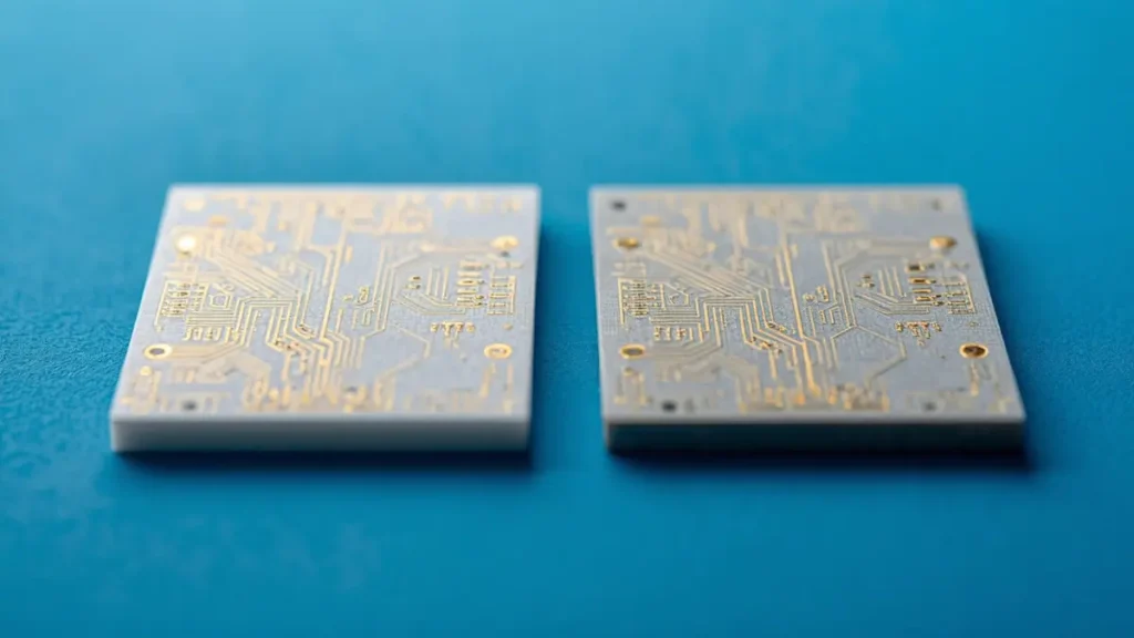
High-Precision Custom Ceramic Circuit Board Fabrication | Hongda Circuit
Selecting the proper base ceramic determines the performance boundaries of the completed electronic assembly:
- Alumina (Al2O3 Ceramic PCB): The industry’s standard cost-effective ceramic substrate. Alumina features a thermal conductivity range of 20-30 W/m-K, providing excellent mechanical ruggedness and high insulation properties at a practical price point for standard industrial sensors and automotive assemblies.
- Aluminum Nitride (AlN Ceramic PCB): The premium choice for high thermal performance. Delivering a thermal conductivity of 170-230 W/m-K, its coefficient of thermal expansion matches silicon closely (about 4.5 ppm/degC). This minimizes mechanical strain on joints, making it the default option for high-power IGBT modules and laser diodes.
- Silicon Nitride (Si3N4 Ceramic Substrate): Engineered for extreme physical reliability. While providing intermediate thermal metrics (about 70-90 W/m-K), it delivers exceptional fracture toughness and resistance to thermal shock, tailored for harsh aerospace deployments and electric vehicle powertrains.
What Are the Differences Between DBC, DPC, and Thick Film Processes?
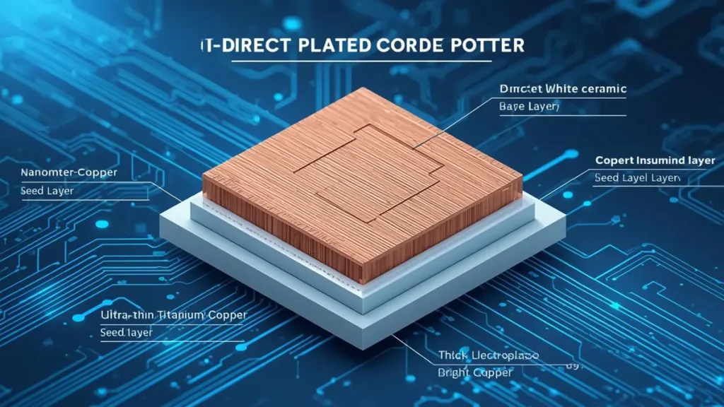
DPC Custom Ceramic Circuit Board Layer Cross-Section Diagram
Choosing the correct metallization method alters trace precision and current-handling capacities:
- Direct Bonded Copper (DBC): Fuses thick, pre-engineered copper foils to substrates via a high-temperature copper-oxygen eutectic reaction. It handles massive current densities, though line widths remain limited to wider spaces (greater than or equal to 150 um).
- Direct Plated Copper (DPC): Utilizes thin-film vacuum magnetron sputtering paired with precision electroplating. It allows exceptionally tight trace distribution (down to 50 um or less lines/spaces), making it perfect for high-density interconnects, fine-pitch flip-chips, and space-constrained optoelectronics.
- Thick Film Processing: Deposits specialized conductive pastes onto substrates using precision screen-printing methods, followed by high-temperature firing. It remains highly cost-effective for simple, low-layer layouts.
How Many Layers Is a Ceramic PCB?
What Is the Maximum Layer Count for Ceramic PCBs?
Standard ceramic circuit deployments focus primarily on single-layer and double-sided topologies. Advanced high-density applications utilize multi-layer structures, though layer limits are tighter than traditional FR4 builds due to the physical characteristics of working with solid, brittle ceramic materials.
Why Are Ceramic PCBs Usually Low Layer Count?
Low layer distributions stem directly from manufacturing complexities and material behavior:
- Thermal Expansion Mismatch: Compounding multiple conductive metal layers against rigid ceramic bases creates internal stress, running the risk of warp or delamination during high-temperature operations.
- Processing Complexity: Drilling deep micro-vias through hardened ceramic requires advanced diamond tooling or specialized lasers, increasing processing time.
- Cost Restrictions: High-temperature processing furnaces and multi-stage vacuum lamination equipment require significant manufacturing resources, focusing multi-layer deployment on high-priority performance applications.
Can Multilayer Ceramic PCBs Be Manufactured?
Yes. True multi-layer ceramic designs are achieved using advanced co-fired technology, categorized into two standard industrial methodologies:
- Low-Temperature Co-fired Ceramic (LTCC): Raw glass-ceramic green tapes are cast, patterned with conductive pastes (such as gold or silver), laminated under pressure, and fired at about 850-900 degC. This allows developers to embed passive components directly inside internal layers, optimizing RF and 5G front-end layouts.
- High-Temperature Co-fired Ceramic (HTCC): Pure ceramic matrices are processed with high-melting refractory metals (like tungsten or molybdenum) and fired at extreme settings (about 1500-1600 degC), delivering exceptional mechanical stability for high-reliability aerospace housings.
How Thick Is the Gold or Copper Conductor on Ceramic PCBs?
What Is the Typical Thickness of Gold Conductors?
Gold layer specs are tailored based on the chosen deposition line and application requirements:
- Thick-Film Gold Paste: Delivers depths between 5-15 um through screen printing and firing, providing a reliable metallurgy for gold-wire bonding.
- Thin-Film / DPC Lines: Utilizes thin-film vacuum magnetron sputtering to deposit an ultra-thin nanometer-scale seed layer (typically Ti/Cu or Ti/W, around 0.1-0.2 um) to ensure strong adhesion. The actual functional conductor trace is then built up via 电镀 (electroplating) (typically 10-75 um for copper). Final gold wire-bonding layers or pads are achieved using an automated ENIG or ENEPIG line (depositing 0.05-0.5 um of gold), ensuring high-frequency signal clarity and preventing trace oxidation without wasting precious metals in sputtering chambers.
What Is the Typical Copper Thickness in DBC Ceramic PCBs?
DBC manufacturing utilizes heavy copper foils, typically running from 100 um up to 600 um. These heavy copper distributions deliver low electrical resistance, turning the PCB into a structural heatsink for high-voltage industrial inverters and EV power stacks.
How Does Conductor Thickness Affect Performance?
Conductor thickness directly shifts primary electronic performance metrics:
- Current Carrying Capacity: Thicker copper layers easily carry hundreds of amperes without generating excessive heat.
- Thermal Dissipation: Thick copper structures distribute heat quickly across the X-Y plane, minimizing local hot spots.
- Signal Integrity: Fine, flat thin-film tracking minimizes high-frequency skin-effect losses, ensuring clean transmission in high-frequency RF paths.
Ceramic PCB Layout Guidelines
What Are the Key Design Rules for Ceramic PCBs?
Ceramic layouts require precise dimensional control. Minimum trace widths and spacing for DPC lines drop down to 50 um, while DBC heavy-copper layouts require wider gaps of 200-300 um to prevent manufacturing defects during etching. Via configurations require clean laser-drilled profiles to avoid micro-cracks, and pad footprints must accommodate proper structural solder fillets during high-temperature reflow cycles.
How to Optimize Thermal Management in Layout?
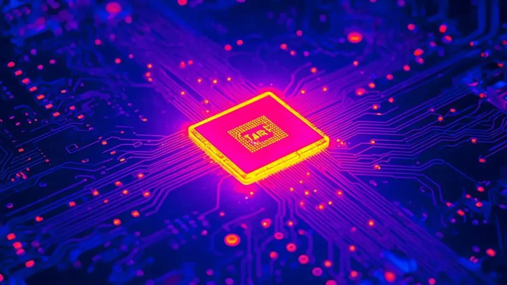
Thermal Dissipation Performance of AlN Custom Ceramic Circuit Board
To leverage the high thermal dissipation of ceramic substrates, designers should use wide copper planes to distribute heat evenly. Placing components with high thermal outputs near the center of the substrate helps avoid edge thermal stress, while direct copper paths underneath thermal pads clear paths for rapid heat dissipation.
What Are Common Layout Mistakes to Avoid?
Avoid using sharp 90-degree trace angles, which can trap chemical etchants and create structural stress concentration points during thermal cycling. Ensure even copper balancing across the top and bottom faces to prevent warping during cooling, and maintain safe clearance distances near edges to eliminate micro-fractures during mechanical panel routing or dicing.
How Does Material Choice Affect Layout Design?
High-wattage layouts with concentrated heat profiles benefit from the 170-230 W/mK performance of Aluminum Nitride (AlN). Standard designs looking for a balance between thermal performance and cost can utilize Alumina (Al2O3). For assemblies subject to severe industrial vibration, Silicon Nitride’s (Si3N4) high fracture toughness provides excellent structural protection.
Substrate Material Performance Comparison
| Comparison Factor | Standard FR4 PCB | MCPCB (Metal-Core) | Alumina Ceramic (Al2O3) | Aluminum Nitride (AlN) |
| Thermal Conductivity (W/m-K) | about 0.3 | 1.0-4.0 | 20-30 | 170-230 |
| High-Frequency Signal Loss | High | Moderate | Low | Very Low |
| CTE Match to Silicon (ppm/degC) | 14-17 (Poor) | 11-15 (Moderate) | 6.5-7.2 (Good) | 4.5-4.8 (Excellent) |
| Max Temperature Resistance | 130 degC or less | 180 degC or less | greater than 300 degC | greater than 300 degC |
| Relative Cost Structure | Baseline Low | Moderate | Medium-High | Premium |
Advanced Manufacturing Capabilities
As a professional ceramic PCB manufacturer, Shenzhen Hongda Circuit Technology Co., Ltd. operates precision DPC and DBC manufacturing lines. Our production workflow combines vacuum sputtering, high-temperature eutectic bonding furnaces, and advanced Laser Direct Imaging (LDI) to maintain tight tolerances on brittle substrates. Every batch undergoes strict quality control protocols, including Automated Optical Inspection (AOI), X-ray bond-layer analysis, and rigorous thermal shock testing to ensure reliable performance in demanding environments.
Purchasing Manager’s Technical FAQ Collection
How do I evaluate a ceramic PCB manufacturer in China before placing a volume production order?
Evaluating a supplier requires looking beyond basic equipment lists to check their actual in-house production capabilities. Verify if the factory manages critical processes like thin-film DPC sputtering, heavy-copper DBC bonding, or Active Metal Brazing (AMB) in their own facility rather than outsourcing them. Always request documented validation reports, including automated optical inspection (AOI) metrics, X-ray bond-integrity scans, and thermal shock testing logs. Sourcing managers should start with a small prototype run to verify actual line tolerances and bond strength before moving forward with full production tooling.
What is the difference between an AlN ceramic PCB supplier and an Alumina ceramic PCB supplier?
The distinction lies in the raw materials they process and the target applications they support. An Alumina-focused supplier typically provides cost-effective boards for standard LED matrices and general industrial sensors where cost efficiency is prioritized over high thermal performance. In contrast, an AlN ceramic PCB supplier works with high-conductivity aluminum nitride matrices (170-230 W/m K) tailored for demanding applications like high-power IGBT modules, traction inverters, and RF assemblies. Ensure your chosen manufacturing partner stocks the specific material grade and thickness required for your design’s thermal profile.
Can Chinese ceramic PCB suppliers handle low-volume prototype orders alongside automated online quotes?
Yes, established manufacturers like Shenzhen Hongda Circuit Technology Co., Ltd. provide dedicated small-batch prototyping services alongside fast online quoting options. These specialized short-run lines allow engineering teams to quickly test and validate physical thermal behavior and electrical performance before investing in long-run production tooling. Technical files submitted through online quote portals undergo a thorough Design for Manufacturing (DFM) review to catch potential structural risks early in the process
What specific quality certifications should a technical buyer require from a ceramic PCB supplier?
At a minimum, buyers should require certified compliance with ISO 9001 quality management standards. Because ceramic substrates are brittle and require specialized processing, standard laminate PCB certifications are not enough. Ensure your supplier provides specialized in-house quality control testing, including non-destructive acoustic or X-ray imaging to check for voiding in DBC layers, along with rigorous thermal shock testing to ensure the long-term reliability of metal-to-ceramic bonds under real-world conditions.
Why is the total ceramic PCB price higher than standard FR4 options, and how can engineering teams control project costs?
Ceramic PCB prices reflect the higher costs of raw materials like pure AlN or Al2O3, as well as the advanced manufacturing methods required, such as vacuum sputtering, high-temperature sintering, and laser patterning. To manage project costs effectively, align your material selection directly with your design’s actual thermal requirements. Use cost-effective Alumina for mid-range thermal applications, and save premium Aluminum Nitride for high-wattage hot spots. Engaging your manufacturer early during the DFM process helps optimize layer structures and panel layout efficiency before final production
About Author
David Chen https://www.linkedin.com/in/pcbcoming
David Chen boasts an extensive professional background in PCBA manufacturing, PCBA testing, and PCBA optimization, with specialized expertise in high-precision PCBA fault analysis and rigorous PCBA reliability testing. The author has worked with high-layer-count server PCB fabrication, ultra-low-loss backplane stackups, and thermo-mechanical reliability optimization for AI infrastructure projects involving 112G and 224G PAM4 architectures. Skilled in complex circuit design and cutting-edge advanced PCB manufacturing processes, he delivers solutions that elevate product durability and performance across industrial applications. His technical articles focusing on PCBA manufacturing workflows and testing methodologies are widely cited by industry peers, research institutions, and technical platforms, solidifying his reputation as a recognized technical authority in the global circuit board manufacturing sector.